US10566345B2 - Three-dimensional semiconductor memory device - Google Patents
Three-dimensional semiconductor memory device Download PDFInfo
- Publication number
- US10566345B2 US10566345B2 US16/018,199 US201816018199A US10566345B2 US 10566345 B2 US10566345 B2 US 10566345B2 US 201816018199 A US201816018199 A US 201816018199A US 10566345 B2 US10566345 B2 US 10566345B2
- Authority
- US
- United States
- Prior art keywords
- electrode structures
- gate insulation
- semiconductor layer
- insulation regions
- electrode
- Prior art date
- Legal status (The legal status is an assumption and is not a legal conclusion. Google has not performed a legal analysis and makes no representation as to the accuracy of the status listed.)
- Active
Links
Images


Classifications
-
- H—ELECTRICITY
- H10—SEMICONDUCTOR DEVICES; ELECTRIC SOLID-STATE DEVICES NOT OTHERWISE PROVIDED FOR
- H10B—ELECTRONIC MEMORY DEVICES
- H10B43/00—EEPROM devices comprising charge-trapping gate insulators
- H10B43/20—EEPROM devices comprising charge-trapping gate insulators characterised by three-dimensional arrangements, e.g. with cells on different height levels
- H10B43/23—EEPROM devices comprising charge-trapping gate insulators characterised by three-dimensional arrangements, e.g. with cells on different height levels with source and drain on different levels, e.g. with sloping channels
- H10B43/27—EEPROM devices comprising charge-trapping gate insulators characterised by three-dimensional arrangements, e.g. with cells on different height levels with source and drain on different levels, e.g. with sloping channels the channels comprising vertical portions, e.g. U-shaped channels
-
- H—ELECTRICITY
- H10—SEMICONDUCTOR DEVICES; ELECTRIC SOLID-STATE DEVICES NOT OTHERWISE PROVIDED FOR
- H10B—ELECTRONIC MEMORY DEVICES
- H10B41/00—Electrically erasable-and-programmable ROM [EEPROM] devices comprising floating gates
- H10B41/20—Electrically erasable-and-programmable ROM [EEPROM] devices comprising floating gates characterised by three-dimensional arrangements, e.g. with cells on different height levels
-
- H01L27/11582—
-
- G—PHYSICS
- G11—INFORMATION STORAGE
- G11C—STATIC STORES
- G11C8/00—Arrangements for selecting an address in a digital store
- G11C8/14—Word line organisation; Word line lay-out
-
- H01L27/1157—
-
- H01L27/11573—
-
- H—ELECTRICITY
- H10—SEMICONDUCTOR DEVICES; ELECTRIC SOLID-STATE DEVICES NOT OTHERWISE PROVIDED FOR
- H10B—ELECTRONIC MEMORY DEVICES
- H10B41/00—Electrically erasable-and-programmable ROM [EEPROM] devices comprising floating gates
- H10B41/30—Electrically erasable-and-programmable ROM [EEPROM] devices comprising floating gates characterised by the memory core region
- H10B41/35—Electrically erasable-and-programmable ROM [EEPROM] devices comprising floating gates characterised by the memory core region with a cell select transistor, e.g. NAND
-
- H—ELECTRICITY
- H10—SEMICONDUCTOR DEVICES; ELECTRIC SOLID-STATE DEVICES NOT OTHERWISE PROVIDED FOR
- H10B—ELECTRONIC MEMORY DEVICES
- H10B43/00—EEPROM devices comprising charge-trapping gate insulators
- H10B43/10—EEPROM devices comprising charge-trapping gate insulators characterised by the top-view layout
-
- H—ELECTRICITY
- H10—SEMICONDUCTOR DEVICES; ELECTRIC SOLID-STATE DEVICES NOT OTHERWISE PROVIDED FOR
- H10B—ELECTRONIC MEMORY DEVICES
- H10B43/00—EEPROM devices comprising charge-trapping gate insulators
- H10B43/20—EEPROM devices comprising charge-trapping gate insulators characterised by three-dimensional arrangements, e.g. with cells on different height levels
-
- H—ELECTRICITY
- H10—SEMICONDUCTOR DEVICES; ELECTRIC SOLID-STATE DEVICES NOT OTHERWISE PROVIDED FOR
- H10B—ELECTRONIC MEMORY DEVICES
- H10B43/00—EEPROM devices comprising charge-trapping gate insulators
- H10B43/30—EEPROM devices comprising charge-trapping gate insulators characterised by the memory core region
- H10B43/35—EEPROM devices comprising charge-trapping gate insulators characterised by the memory core region with cell select transistors, e.g. NAND
-
- H—ELECTRICITY
- H10—SEMICONDUCTOR DEVICES; ELECTRIC SOLID-STATE DEVICES NOT OTHERWISE PROVIDED FOR
- H10B—ELECTRONIC MEMORY DEVICES
- H10B43/00—EEPROM devices comprising charge-trapping gate insulators
- H10B43/40—EEPROM devices comprising charge-trapping gate insulators characterised by the peripheral circuit region
-
- H—ELECTRICITY
- H10—SEMICONDUCTOR DEVICES; ELECTRIC SOLID-STATE DEVICES NOT OTHERWISE PROVIDED FOR
- H10B—ELECTRONIC MEMORY DEVICES
- H10B43/00—EEPROM devices comprising charge-trapping gate insulators
- H10B43/50—EEPROM devices comprising charge-trapping gate insulators characterised by the boundary region between the core and peripheral circuit regions
Definitions
- Exemplary embodiments of the present inventive concept relate to a memory device, and more particularly to a three-dimensional semiconductor memory device.
- Semiconductor devices may be relatively highly integrated and may be manufactured at relatively low manufacturing costs. Integration density of semiconductor devices may be a factor in determining product price. Integration of typical two-dimensional or planar semiconductor devices may be determined by the area occupied by a unit memory cell, and thus integration of two-dimensional or planar semiconductor devices may be influenced by the level of technology for forming fine patterns. Processing equipment used to increase pattern fineness may limit integration density of the two-dimensional or planar semiconductor devices. Three-dimensional semiconductor memory devices may have three-dimensionally arranged memory cells.
- An exemplary embodiment of the present inventive concept provides a three-dimensional semiconductor memory device having increased reliability and integration.
- a three-dimensional semiconductor memory device includes a peripheral logic structure on a semiconductor substrate.
- a horizontal semiconductor layer is on the peripheral logic structure and includes a cell array region and a connection region.
- Electrode structures extend in a first direction on the horizontal semiconductor layer and are spaced apart in a second direction intersecting the first direction.
- a pair of the electrode structures adjacent to each other are symmetrically disposed to define a contact region partially exposing the horizontal semiconductor layer.
- a through via structure is on the contact region and connects the electrode structures to the peripheral logic structure.
- Each of the electrode structures include a plurality of gate insulation regions extending along the first direction on the connection region. The gate insulation regions have different lengths from each other in the first direction.
- a three-dimensional semiconductor memory device includes a peripheral logic structure on a semiconductor substrate.
- a horizontal semiconductor layer is on the peripheral logic structure and includes a cell array region and a connection region.
- Electrode structures extend in a first direction on the horizontal semiconductor layer and are spaced apart in a second direction intersecting the first direction.
- a through via structure penetrates the electrode structures and the horizontal semiconductor layer. The through via structure connects the electrode structures to the peripheral logic structure.
- Each of the electrode structures include first gate insulation regions extending in the first direction on the cell array region and spaced apart from each other at a first interval.
- Each of the electrode structures include second gate insulation regions extending in the first direction on the connection region and spaced apart from each other at a second interval less than the first interval.
- a three-dimensional semiconductor memory device includes a peripheral logic structure on a semiconductor substrate.
- a horizontal semiconductor layer is on the peripheral logic structure and includes a cell array region and a connection region.
- Electrode structures extend in a first direction on the horizontal semiconductor layer and are spaced apart in a second direction intersecting the first direction.
- Each of the electrode structures include first gate insulation regions extending in the first direction on the cell array region and spaced apart from each other at a first interval.
- Each of the electrode structures include second gate insulation regions spaced apart from the first gate insulation regions and extending in the first direction on the connection region.
- the second gate insulation regions are spaced apart from each other at a second interval less than the first interval.
- Gate openings are provided between ground select gate electrodes in the second direction and between the first gate insulation regions and the second gate insulation regions in the first direction. The ground select gate electrodes are spaced apart from each other in the second direction at a same level from the horizontal semiconductor layer.
- a three-dimensional semiconductor memory device includes a peripheral logic structure on a semiconductor substrate.
- a horizontal semiconductor layer is on the peripheral logic structure and includes a cell array region and a connection region.
- a through via structure partially penetrates the horizontal semiconductor layer on the connection region.
- An electrode structure is on the horizontal semiconductor layer and extends in a first direction. A portion of the electrode structure surrounds the through via structure on the connection region.
- the electrode structure includes a plurality of ground select gate electrodes separated from each other in a second direction crossing the first direction at a same level from the horizontal semiconductor layer as each other.
- Each of the ground select gate electrodes have a first width on the cell array region and a second width on an area adjacent to the through via structure. The second width is less than the first width.
- a semiconductor memory device includes a semiconductor substrate including a cell array region and a connection region.
- a peripheral logic structure is disposed on the semiconductor substrate.
- a plurality of ground select lines are stacked in the cell array region. The ground select lines are spaced apart from each other by first insulating layers.
- a plurality of word lines are stacked on the ground select lines in the cell array region. The word lines are spaced apart from each other by second insulating layers. The plurality of word lines form a stepped structure.
- a vertical structure penetrates the plurality of word lines and the plurality of ground select lines. The vertical structure is connected to a lowermost ground select line of the plurality of ground select lines.
- a through via structure is in the connection region. The through via structure connects the plurality of ground select lines and the plurality of word lines to the peripheral logic structure.
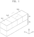
- FIG. 1 is a perspective view of a three-dimensional semiconductor memory device according to an exemplary embodiment of the present inventive concept.
- FIG. 2 is a circuit diagram of a cell array of a three-dimensional semiconductor memory device according to an exemplary embodiment of the present inventive concept.
- FIGS. 3A and 3B are plan views of a three-dimensional semiconductor memory device according to an exemplary embodiment of the present inventive concept.
- FIG. 4 is a plan view of a cell array structure of a three-dimensional semiconductor memory device according to an exemplary embodiment of the present inventive concept.
- FIG. 5 is an enlarged view of section A of FIG. 4 .
- FIG. 6 is a cross-sectional view of a three-dimensional semiconductor memory device according to an exemplary embodiment of the present inventive concept.
- FIGS. 7A and 7B are enlarged views of section B of FIG. 6 .
- FIG. 8 is a plan view of ground select gate electrodes included in an electrode structure according to an exemplary embodiment of the present inventive concept.
- FIG. 9 is a plan view of a cell gate electrode included in an electrode structure according to an exemplary embodiment of the present inventive concept.
- FIGS. 10 and 11 are plan views of a three-dimensional semiconductor memory device according to an exemplary embodiment of the present inventive concept.
- FIG. 12 is a plan view of a cell array structure of a three-dimensional semiconductor memory device according to an exemplary embodiment of the present inventive concept.
- FIG. 13 is an enlarged view of section A of FIG. 12 .
- FIG. 14 is a plan view of ground select gate electrodes included in an electrode structure according to an exemplary embodiment of the present inventive concept.
- FIG. 15 is a plan view of a cell gate electrode included in an electrode structure according to an exemplary embodiment of the present inventive concept.
- FIG. 16 is a plan view of a three-dimensional semiconductor memory device according to an exemplary embodiment of the present inventive concept.
- FIGS. 17A, 18A, 19A, 20A, 21, and 22 are cross-sectional views of a method of manufacturing a three-dimensional semiconductor memory device according to an exemplary embodiment of the present inventive concept.
- FIGS. 17B, 18B, 19B, 20B, 17C, 18C, 19C and 20C are plan views of a method of manufacturing a three-dimensional semiconductor memory device according to an exemplary embodiment of the present inventive concept.
- FIG. 1 is a perspective view of a three-dimensional semiconductor memory device according to an exemplary embodiment of the present inventive concept.
- a three-dimensional semiconductor memory device may include a peripheral logic structure PS and a cell array structure CS, which is stacked on the peripheral logic structure PS.
- the peripheral logic structure PS and the cell array structure CS may overlap each other.
- the first and second directions D 1 and D 2 may be perpendicular to each other.
- the peripheral logic structure PS may include a page buffer, a control circuit, and row and column decoders that control a cell array of a three-dimensional semiconductor memory device.
- the cell array structure CS may include a plurality of memory blocks BLK 1 to BLKn each of which may be a data erasure unit.
- Each of the memory blocks BLK 1 to BLKn may include a memory cell array having a three-dimensional structure.
- Each of the memory blocks BLK 1 to BLKn may include a memory cell array having a vertical structure.
- the memory cell array may include three-dimensionally arranged memory cells and a plurality of word lines and bit lines electrically connected to the memory cells. As an example, the memory cell array having the three-dimensional structure will be discussed below in more detail with reference to the accompanying drawings.
- FIG. 2 is a circuit diagram of a cell array of a three-dimensional semiconductor memory device according to an exemplary embodiment of the present inventive concept.
- a cell array of a three-dimensional semiconductor memory device may include a common source line CSL, a plurality of bit lines BL 0 to BL 2 , and a plurality of cell strings CSTR between the common source line CSL and the bit lines BL 0 to BL 2 .
- the cell strings CSTR may extend along the third direction D 3 (e.g., along a plane elongated from first and second directions D and D 2 ).
- the bit lines BL 0 to BL 2 may be spaced apart from each other in the first direction D 1 , and may extend in the second direction D 2 .
- a plurality of cell strings CSTR may be connected in parallel to each of the bit lines BL 0 to BL 2 .
- the plurality of cell strings CSTR may be commonly connected to the common source line CSL.
- a plurality of cell strings CSTR may be disposed between a plurality of bit lines BL 0 to BL 2 and one common source line CSL.
- the common source line CSL may include a plurality of common source lines CSL, and the plurality of common source lines CSL may be two-dimensionally arranged.
- the common source lines CSL may extend along the first and second direction D 1 and D 2 .
- the common source lines may extend along only one of the first direction D 1 or the second direction D 2 .
- the common source lines CSL may be supplied with the same voltage as each other or may be electrically controlled independently of each other. Thus, a different voltage may be applied to each of the common source lines CSL.
- each of the cell strings CSTR may include string select transistors SST 1 and SST 2 connected in series, memory cells MCT connected in series, and a ground select transistor GST.
- Each of the memory cells MCT may include a data storage element.
- each of the cell strings CSTR may include first and second string select transistors SST 1 and SST 2 connected in series.
- the second string select transistor SST 2 may be coupled to (e.g., may be electrically connected to) one of the bit lines BL 0 to BL 2
- the ground select transistor GST may be coupled to (e.g., may be electrically connected to) the common source line CSL.
- the memory cells MCT may be connected in series between the first string select transistor SST 1 and the ground select transistor GST.
- Each of the cell strings CSTR may include a dummy cell DMC connected between the first string select transistor SST 1 and the memory cell MCT.
- the dummy cell DMC may also be connected between the ground select transistor GST and the memory cell MCT.
- the ground select transistor GST may include a plurality of MOS transistors connected in series in each of the cell strings CSTR.
- each of the cell strings CSTR may include a single string select transistor.
- the first string select transistor SST 1 may be controlled by a first string select line SSL 1
- the second string select transistor SST 2 may be controlled by a second string select line SSL 2
- the memory cells MCT may be controlled by a plurality of word lines WL 0 to WLn
- the dummy cells DMC may be controlled by a dummy word line DWL
- the ground select transistor GST may be controlled by a corresponding one of ground select lines GSL 0 to GSL 2 .
- the common source line CSL may be connected in common to sources of the ground select transistors GST.
- the ground select lines may each include cell gate electrodes (e.g., cell gate electrodes CGE, which are described in more detail below).
- the ground select lines may be vertically stacked above the semiconductor substrate.
- a plurality of word lines may be stacked on the ground select lines to form a stepped structure above the ground select lines.
- Each of the ground select lines and the word lines may be electrically connected to the peripheral logic structure (e.g., by the through via structure TVS) described herein.
- a single cell string CSTR may include a plurality of memory cells MCT that are spaced apart from the common source line CSL at different distances.
- the plurality of memory cells MCT may be spaced apart from each other along the first direction D 1 .
- a plurality of word lines WL 0 to WLn and DWL may be disposed between the common source lines CSL and the bit lines BL 0 to BL 2 .
- the memory cells MCT may include gate electrodes at substantially the same distance from the common source lines CSL, and the gate electrodes may be connected in common to one of the word lines WL 0 to WLn and DWL, thus being in an equipotential state.
- the gate electrodes of the memory cells MCT may be at substantially the same distance from the common source lines CSL, the gate electrodes disposed at different rows or columns may be independently controlled. Thus, different voltages may be applied to each of the gate electrodes.
- the ground select lines GSL 0 to GSL 2 and the string select lines SSL 1 and SSL 2 may extend along the first direction D 1 and may be spaced apart from each other in the second direction D 2 .
- the ground select lines GSL 0 to GSL 2 may be located at substantially the same level from the common source lines CSL, thus being electrically separated from each other.
- the same may be true of the string select lines SSL 1 and SSL 2 .
- each of the ground select lines may be positioned at an equal distance as each other above the common source line CSL.
- FIGS. 3A and 3B are plan views of a three-dimensional semiconductor memory device according to an exemplary embodiment of the present inventive concept.
- a three-dimensional semiconductor memory device may include the peripheral logic structure PS on a semiconductor substrate 10 , a cell array structure (e.g., cell array structure CS described above with reference to FIG. 1 ) on the peripheral logic structure PS, and a through via structure TVS that connects the cell array structure CS and the peripheral logic structure PS to each other.
- a cell array structure e.g., cell array structure CS described above with reference to FIG. 1
- a through via structure TVS that connects the cell array structure CS and the peripheral logic structure PS to each other.
- the peripheral logic structure PS may include peripheral logic circuits that process data communicated with a three-dimensional cell array.
- the cell array structure CS may include a plurality of electrode structures ST on a horizontal semiconductor layer 100 and a plurality of vertical structures VS penetrating each of the electrode structures ST.
- the cell array structure CS when viewed in a plan view, may overlap the peripheral logic structure PS (see, e.g., FIG. 1 ).
- the cell array structure may overlap the peripheral logic structure PS along the third direction D 3 .
- the horizontal semiconductor layer 100 may include a cell array region CAR on which memory cells are provided and a connection region CNR to which contact plugs and conductive lines coupled to the memory cells are connected.
- the electrode structures ST may extend in the first direction D 1 on the horizontal semiconductor layer 100 .
- Adjacent electrode structures ST may be spaced apart from each other by an electrode separation region ESR that separates the adjacent electrode structures ST from each other in the second direction D 2 intersecting the first direction D 1 .
- the second direction D 2 may be perpendicular to the first direction D 1 .
- each of the electrode structures ST may include a first line part having a first width W 1 and a second line part having a second width W 2 less than the first width W 1 .
- Adjacent electrode structures ST may be disposed such that their second line parts may face each other.
- a pair of adjacent electrode structures ST may be disposed mirror-symmetrically to each other to define at least one contact region (see, e.g., the region defined by a through via structure TVS in FIG. 6 ) that partially exposes the horizontal semiconductor layer 100 .
- the contact region may be defined between the second line parts of two adjacent electrode structures ST.
- the electrode structures ST may define more than one contact region. Referring to FIG. 3B , a pair of adjacent electrode structures ST may define a plurality of contact regions spaced apart from each other in the first direction D 1 .
- the through via structure TVS may be provided on the contact region defined by a pair of electrode structures ST.
- one or more through via structures TVS may be provided between the second line parts of a pair of electrode structures ST.
- FIG. 4 is a plan view of a cell array structure of a three-dimensional semiconductor memory device according to an exemplary embodiment of the present inventive concept.
- FIG. 5 is an enlarged view of section A of FIG. 4 .
- FIG. 6 is a cross-sectional view of a three-dimensional semiconductor memory device according to an exemplary embodiment of the present inventive concept.
- FIGS. 7A and 7B are enlarged views of section B of FIG. 6 .
- FIG. 8 is a plan view of ground select gate electrodes included in an electrode structure according to an exemplary embodiment of the present inventive concept.
- FIG. 9 is a plan view of a cell gate electrode included in an electrode structure according to an exemplary embodiment of the present inventive concept.
- the peripheral logic structure PS may include peripheral logic circuits PTR disposed on the semiconductor substrate 10 and a lower buried insulating layer 50 covering the peripheral logic circuits PTR.
- a plurality of peripheral logic circuits PTR may be disposed on the semiconductor substrate, and may be spaced apart from each other along the first direction D 1 .
- the peripheral logic circuits PTR may be in direct contact with an upper surface of the semiconductor substrate.
- the peripheral logic circuits PTR may each be disposed on a source or drain region (e.g., source/drain regions 25 ) formed in the semiconductor substrate 10 .
- the semiconductor substrate 10 may be or include a silicon substrate, a silicon-germanium substrate, a germanium substrate, or a single crystalline epitaxial layer grown on a single crystalline silicon substrate.
- the peripheral logic circuits PTR may be, as discussed above, row and column decoders, a page buffer, or a control circuit, and may include NMOS or PMOS transistors, low-voltage or high-voltage transistors, and a resistor that are integrated on the semiconductor substrate 10 .
- the semiconductor substrate 10 may be provided therein with a device isolation layer 11 that defines active regions.
- the active regions of the semiconductor substrate 10 may be provided thereon with peripheral gate electrodes 23 and gate dielectric layers 21 disposed between the peripheral gate electrodes 23 and the semiconductor substrate 10 .
- Source/drain regions 25 may be provided in the semiconductor substrate 10 on opposite sides of each of the peripheral gate electrodes 23 .
- Peripheral circuit lines 33 may be electrically connected through peripheral circuit contact plugs 31 to the peripheral logic circuits PTR.
- the peripheral circuit contact plugs 31 and the peripheral circuit lines 33 may be coupled to the NMOS and PMOS transistors.
- the lower buried insulating layer 50 may cover the peripheral logic circuits PTR (e.g., may be disposed on side surfaces of the peripheral logic circuits PTR), the peripheral circuit contact plugs 31 , and the peripheral circuit lines 33 .
- the lower buried insulating layer 50 may include a plurality of stacked insulating layers.
- the lower buried insulating layer 50 may include a silicon oxide layer, a silicon nitride layer, a silicon oxynitride layer, or a low-k dielectric layer.
- the cell array structure CS may be disposed on the lower buried insulating layer 50 , and may include the horizontal semiconductor layer 100 , the electrode structures ST, and the vertical structures VS.
- the horizontal semiconductor layer 100 may include a semiconductor material including, for example, silicon (Si), germanium (Ge), silicon germanium (SiGe), gallium arsenic (GaAs), indium gallium arsenic (InGaAs), aluminum gallium arsenic (AlGaAs), or a mixture thereof. Additionally or alternatively, the horizontal semiconductor layer 100 may include either semiconductor doped with a first conductivity impurity or intrinsic semiconductor doped with no impurity. Additionally or alternatively, the horizontal semiconductor layer 100 may have a crystal structure including one or more of a single crystalline structure, an amorphous structure, or a polycrystalline structure.
- the horizontal semiconductor layer 100 may include the cell array region CAR and the connection region CNR around the cell array region CAR.
- the cell strings CSTR (see, e.g., FIG. 2 ) may be integrated on the cell array region CAR of the horizontal semiconductor layer 100 .
- a plurality of electrode structures ST may be disposed on the horizontal semiconductor layer 100 .
- the electrode structures ST may extend along the first direction D 1 from the cell array region CAR toward the connection region CNR.
- the electrode structures ST may be spaced apart from each other in the second direction D 2 .
- Each of the electrode structures ST may include electrodes GGE, CGE, and SGE and insulating layers ILD 1 and ILD 2 that are alternately stacked along the third direction D 3 (e.g., a vertical direction with respect to an upper surface of the horizontal semiconductor layer 100 ) perpendicular to the first and second directions D 1 and D 2 .
- each of the electrode structures ST may include a plurality of cell gate electrodes CGE that are vertically stacked, a plurality of ground select gate electrodes GGE that are horizontally spaced apart from each other beneath a lowermost cell gate electrode CGE, and a plurality of string select gate electrodes SGE that are horizontally spaced apart from each other above an uppermost cell gate electrode CGE.
- Each of the electrode structures ST may have a structure where the plurality of ground select gate electrodes GGE are located at the same level from a top surface of the horizontal semiconductor layer 100 as each other and the plurality of cell gate electrodes CGE are located at different levels from the top surface of the horizontal semiconductor layer 100 from each other.
- the ground select gate electrodes GGE may each include ground select lines (e.g., ground select lines GSL described in more detail above).
- the cell gate electrodes CGE may each include word lines (e.g., word lines WL described in more detail above).
- lowermost ground select gate electrodes GGE may serve as gate electrodes of the ground select transistors (e.g., GST of FIG. 2 ) that control electrical connections between the common source line (e.g., CSL of FIG. 2 ) and the vertical structures VS.
- Uppermost string select gate electrodes SGE may serve as gate electrodes of the string select transistors (e.g., SST of FIG. 2 ) that control electrical connections between the vertical structures VS and a bit line BL.
- the bit line BL may be positioned above the string select electrodes SGE.
- the cell gate electrodes CGE may serve as the control gate electrodes (e.g., WL 0 to WL 3 and DWL of FIG. 2 ) of the memory cells (e.g., MCT of FIG. 2 ).
- a plurality of vertical structures VS may penetrate the electrode structure ST to come into contact (e.g., to be electrically connected with) with the horizontal semiconductor layer 100 .
- the vertical structures VS may be arranged, for example, in a straight line (e.g., a matrix shape) or a zigzag pattern.
- the vertical structures VS may include a semiconductor material such as silicon (Si), germanium (Ge), or a mixture thereof. Additionally or alternatively, the vertical structures VS may include impurity-doped semiconductor or undoped intrinsic semiconductor.
- the vertical structures VS including a semiconductor material may serve as channels of the select transistors SST and GST, the memory cells MCT, and the dummy cell DMC described above with reference to FIG. 2 .
- each of the vertical structures VS may include a lower semiconductor pattern LSP and an upper semiconductor pattern USP.
- the lower semiconductor pattern LSP may include an epitaxial layer that is epitaxially grown from the horizontal semiconductor layer 100 .
- the lower semiconductor pattern LSP may have a pillar shape that fills a lower portion of a vertical hole.
- the lower semiconductor pattern LSP may have a top surface higher than that of the lowermost ground select gate electrode GGE.
- the upper semiconductor pattern USP may be connected to the lower semiconductor pattern LSP, and may include silicon (Si), germanium (GE), or a mixture thereof.
- the upper semiconductor pattern USP may be provided on its top end with a bit line conductive pad, which may be an impurity-doped region or may include a conductive material.
- the upper semiconductor pattern USP may include a first semiconductor pattern SP 1 and a second semiconductor pattern SP 2 .
- the first semiconductor pattern SP 1 may be coupled to the lower semiconductor pattern LSP, and may have a cylindrical or pipe shape with a closed bottom end.
- the first semiconductor pattern SP 1 may have an inside substantially filled with a buried insulating pattern VI.
- the first semiconductor pattern SP 1 may electrically connect the second semiconductor pattern SP 2 and the lower semiconductor pattern LSP to each other.
- the second semiconductor pattern SP 2 may have a cylindrical or pipe shape with open top and bottom ends.
- the second semiconductor pattern SP 2 need not be in contact with, but may be spaced apart from, the lower semiconductor pattern LSP.
- each of the vertical structures VS may include a first semiconductor pattern SP 1 and a second semiconductor pattern SP 2 .
- the first semiconductor pattern SP 1 may be in direct contact with the horizontal semiconductor layer 100 , and may have an inside substantially filled with a buried insulating pattern VI.
- a vertical insulating pattern VP may be disposed between the electrode structure ST and the vertical structure VS.
- the vertical insulating pattern VP may have a cylindrical or pipe shape with open top and bottom ends.
- the vertical insulating pattern VP may extend in the third direction D 3 .
- the vertical insulating pattern VP may be disposed on a sidewall and at least part of a bottom surface of the vertical structure VS.
- the vertical insulating pattern VP may at least partially surround the vertical structure VS.
- the vertical structure VS includes the lower and upper semiconductor patterns LSP and USP
- the vertical insulating pattern VP may surround a sidewall of the upper semiconductor pattern USP.
- the vertical insulating pattern VP may be a portion of a data storage layer.
- the vertical insulating pattern VP may include a tunnel insulating layer TIL, a charge storage layer CIL, and a blocking insulating layer BLK, which include a data storage layer of a NAND Flash memory device.
- the charge storage layer CIL may be a trap insulating layer, a floating gate electrode, or an insulating layer including conductive nano-dots.
- the vertical insulating pattern VP may include a thin film for a phase change memory device or variable resistance memory device.
- a horizontal insulating pattern HP may be disposed between the vertical insulating pattern VP and sidewalls of the electrodes GGE, CGE, and SGE, and may extend onto top and bottom surfaces of each of the electrodes GGE, CGE, and SGE.
- the horizontal insulating pattern HP may include a charge storage layer serving as a portion of a data storage layer of an NAND Flash memory device.
- each of the electrode structures ST may be stacked.
- the electrodes GGE, CGE, and SGE (e.g., the electrodes CGE) may have a stepwise structure. Therefore, each of the electrode structures ST may have a height that decreases with increasing distance from the cell array region CAR.
- the electrodes GGE, CGE, and SGE of each of the electrode structures ST may have lengths in the first direction D 1 that decrease with increasing distance from the horizontal semiconductor layer 100 (e.g., along the third direction D 3 ).
- each of the electrode structures ST may include a lower stepwise structure Sa, an intermediate stepwise structure Sb, and an upper stepwise structure Sc that are sequentially provided along the first direction D 1 (see, e.g., FIGS. 4 and 6 ).
- the electrode structure ST may include a lower region, an intermediate region, and an upper region that are sequentially provided along the third direction D 3 perpendicular to the top surface of the horizontal semiconductor layer 100 .
- the lower stepwise structure Sa may include the electrodes GGE and CGE provided on the lower region of the electrode structure ST
- the intermediate stepwise structure Sb may include the electrodes CGE provided on the intermediate region of the electrode structure ST.
- the upper stepwise structure Sc may include the electrodes CGE and SGE provided on the upper region of the electrode structure ST.
- Each of the electrode structures ST may include the first line part having the first width W 1 and the second line part having the second width W 2 (see, e.g., FIGS. 3A and 3B ).
- the through via structure TVS may be provided between the second line parts of a pair of adjacent electrode structures ST.
- the through via structure TVS may include a through insulation pattern 200 that at least partially penetrates the horizontal semiconductor layer 100 and extends in the third direction D 3 to run across portions of sidewalls of the electrode structures ST, a plurality of through plugs TPLG provided in the through insulation pattern 200 , and a plurality of conductive lines CLb coupled to the through plugs TPLG.
- the through insulation pattern 200 may extend in the third direction D 3 on the lower buried insulating layer 50 .
- the through insulation pattern 200 may include an insulating material such as a silicon oxide layer or a low-k dielectric layer. When viewed in a plan view, the through insulation pattern 200 may be adjacent to a pair of electrode structures ST. As an example, sides of the through insulation pattern 200 may be surrounded by electrode structures ST when viewed in a plan view.
- the through insulation pattern 200 may be positioned between the lower and upper stepwise structures Sa and Sc, which may be arranged in the first direction D 1 , of each of the electrode structures ST.
- the through insulation pattern 200 may be between the intermediate stepwise structures Sb, which may be arranged in the second direction D 2 , of a pair of electrode structures ST.
- the upper and lower stepwise structures Sc and Sa of each of the electrode structures ST may be adjacent in the first direction D 1 to the through insulation pattern 200
- the intermediate stepwise structure Sb of each of the electrode structures ST may be adjacent in the second direction D 2 to the through insulation pattern 200 .
- the through insulation pattern 200 may have a bottom surface in direct contact with the lower buried insulating layer 50 of the peripheral logic structure PS and may have a top surface at substantially the same level (e.g., along the third direction D 3 ) as that of top surfaces of the vertical structures VS.
- the through insulation pattern 200 may have a greater height in the third direction D 3 than those of the electrode structures ST.
- the through insulation pattern 200 may have a width (e.g., in the first and/or second direction D 2 or D 3 ) that varies depending on the height of the electrode structure ST.
- the width of the through insulation pattern 200 may be substantially the same as the first width W 1 of the electrode structure ST.
- the through plugs TPLG may penetrate the through insulation pattern 200 and may come into contact with (e.g., may be electrically connected) the peripheral circuit lines 33 of the peripheral logic structure PS.
- the through plugs TPLG may be connected through the conductive lines CLb to the electrodes CGE that are included in the intermediate stepwise structure Sb of the electrode structure ST.
- An upper buried insulating layer 150 may be disposed on side surfaces of the through insulation pattern 200 and stepwise-structured ends of the electrode structures ST.
- First and second interlayer dielectric layers 151 and 153 may be sequentially stacked on the upper buried insulating layer 150 .
- a bit line BL may be formed on the second interlayer dielectric layer 153 .
- the bit line BL may overlap at least one vertical structure VS (e.g., along the third direction D 3 orthogonal to the first and second directions D 1 and D 2 ).
- Lower contact plugs PLGa may penetrate the upper buried insulating layer 150 and may come into direct contact with the electrodes GGE and CGE that are provided on the lower region of the electrode structure ST to form the lower stepwise structure Sa.
- the lower contact plugs PLGa may be connected to (e.g., may be electrically connected to) connection contact plugs PPLG through first conductive lines CLa extending in the first direction D 1 .
- the connection contact plugs PPLG may penetrate the upper buried insulating layer 150 to come into connection with the peripheral circuit lines 33 of the peripheral logic structure PS.
- Intermediate contact plugs PLGb may penetrate the upper buried insulating layer 150 and may come into direct contact with the electrodes CGE that are provided on the intermediate region of the electrode structure ST to form the intermediate stepwise structure Sb.
- the intermediate contact plugs PLGb may be connected to (e.g., may be electrically connected to) the through plugs TPLG through second conductive lines CLb extending in the second direction D 2 .
- Upper contact plugs PLGc may penetrate the upper buried insulating layer 150 and may come into direct contact with the electrodes CGE and SGE that are provided on the upper region of the electrode structure ST to form the upper stepwise structure Sc.
- the upper contact plugs PLGc may be connected to (e.g., may be electrically connected to) the through plugs TPLG through third conductive lines CLc extending in the first direction D 1 .
- the cell array region CAR may be provided with first gate insulation regions GIR 1 penetrating each of the electrode structures ST, and the connection region CNR may be provided with second gate insulation regions GIR 2 penetrating each of the electrode structures ST.
- the first gate insulation regions GIR 1 may extend substantially parallel to each other in the first direction D 1 .
- the second gate insulation regions GIR 2 may extend substantially parallel to each other (e.g., in the first direction D 1 ).
- the second gate insulation regions GIR 2 may include portions that extend in the second direction D 2 .
- the second gate insulation regions GIR 2 may surround the through insulation pattern 200 (e.g., when viewed in a plan view).
- portions of the second gate insulation regions GIR 2 may be provided on the second line part having the second width W 2 of the electrode structure ST.
- the second gate insulation regions GIR 2 may be configured such that the portions provided on the second line part may have different lengths from each other in the first direction D 1 .
- the first gate insulation regions GIR 1 may be spaced apart in the first direction D 1 from the second gate insulation regions GIR 2 .
- each of the electrode structures ST may have three first gate insulation regions GIR 1 and three second gate insulation regions GIR 2 , exemplary embodiments of the present inventive concept are not limited thereto.
- the number of each of the first and second gate insulation regions GIR 1 and GIR 2 may be changed, for example, on the basis of integration and/or process conditions of a three-dimensional semiconductor memory device.
- connection region CNR may be provided with dummy gate insulation regions DIR penetrating the electrode structures ST.
- the dummy gate insulation regions DIR may have linear shapes extending in the first direction D 1 , and may be spaced apart from the second gate insulation regions GIR 2 .
- the dummy gate insulation regions DIR may be provided on the first line part having the first width W 1 of the electrode structure ST.
- Adjacent electrode structures ST may be provided therebetween with the electrode separation regions ESR, one of which linearly extends from the cell array region CAR toward the connection region CNR. Another one of the electrode separation regions ESR may extend from the cell array region CAR toward the connection region CNR while including portions extending in the second direction D 2 to surround the through insulation pattern 200 .
- Each of the electrode structures ST may be provided with gate openings OP between the lowermost ground select gate electrodes GGE in the second direction D 2 and between the first gate insulation regions GIR 1 and the second gate insulation regions GIR 2 in the first direction D 1 .
- Each of the electrode structures ST may be provided with the gate openings OP provided at the lowermost bottom thereof and with the first and second gate insulation regions GIR 1 and GIR 2 , and thus the lowermost ground select gate electrodes GGE of each of the electrode structures ST may be spaced from each other in the second direction D 2 and may be electrically separated from each other.
- the cell gate electrodes CGE vertically stacked on the ground select gate electrodes GGE may have portions overlapping the gate openings OP, which will be described in more detail below with reference to FIGS. 8 and 9 .
- Common source regions CSR may be provided in the horizontal semiconductor layer 100 beneath the first gate insulation regions GIR 1 penetrating the electrode structures ST.
- the common source regions CSR may extend in the first direction D 1 parallel to the first gate insulation regions GIR 1 .
- the common source regions CSR may include impurities (e.g., N-type impurities such as arsenic (As) or phosphorous (P)) with a conductivity opposite to that of the horizontal semiconductor layer 100 .
- the electrode structure ST may include four ground select gate electrodes GGE 0 , GGE 1 , GGE 2 , and GGE 3 .
- Each of the ground select gate electrodes GGE 0 to GGE 3 may include an electrode portion EP disposed on the cell array region CAR and a pad portion (e.g., first pad portion P 1 ) disposed on the connection region CNR.
- the electrode portion EP of each of the ground select gate electrodes GGE 0 to GGE 3 may extend in the first direction D 1 while having a third width W 3 .
- the pad portion of each of the ground select gate electrodes GGE 0 to GGE 3 may include the first pad portion P 1 extending in the first direction D 1 from the electrode portion EP while having the third width W 3 , a second pad portion P 2 extending in the first direction D 1 while having a fourth width W 4 less than the third width W 3 , and a connection portion CP connecting the first and second pad portions P 1 and P 2 while extending in the second direction D 2 .
- the second pad portions P 2 of the ground select gate electrodes GGE 0 to GGE 3 may have different lengths from each other in the first direction D 1 .
- the ground select gate electrodes GGE 0 to GGE 3 may be configured such that the lengths in the first direction D 1 of the second pad portions P 2 may gradually increase or decrease.
- the dummy gate insulation regions DIR may be provided on the first pad portions P 1 of the ground select gate electrodes GGE 0 to GGE 3 .
- each of the cell gate electrodes CGE may include electrode portions EP disposed on the cell array region CAR, pad portions (e.g., pad portion P 1 ) disposed on the connection region CNR, and an electrode connection portion ECP through which the electrode portions EP and the pad portions are connected to each other.
- the electrode portions EP and the pad portions may be a single continuous body (e.g., including portions extending in the first and second directions D 1 and D 2 ).
- each of the cell gate electrodes CGE may include four electrode portions EP and four pad portions.
- the electrode portions EP of the cell gate electrode CGE may extend in the first direction D 1 while having a substantially uniform third width W 3 on the cell array region CAR.
- Each of the pad portions of the cell gate electrode CGE may extend in the first direction D 1 and have a portion extending in the second direction D 2 .
- each of the pad portions of the cell gate electrode CGE may include the first pad portion P 1 extending in the first direction D 1 from the electrode portion EP while having the third width W 3 , the second pad portion P 2 extending in the first direction D 1 while having the fourth width W 4 less than the third width W 3 , and the connection portion CP connecting the first and second pad portions P 1 and P 2 while extending in the second direction D 2 .
- the second pad portions P 2 may have different lengths from each other in the first direction D 1 .
- the dummy gate insulation regions DIR may be provided on the first pad portions P 1 of the cell gate electrode CGE.
- a semiconductor memory device may include the semiconductor substrate 10 including the cell array region CAR and the connection region CNR (see, e.g., FIG. 3A ).
- the peripheral logic structure PS may be disposed on the semiconductor substrate 10 .
- a plurality of ground select lines (e.g., ground select lines GGE in FIG. 6 ) may be stacked in the cell array region CAR. The ground select lines may be spaced apart from each other by first insulating layers ILD 1 .
- a plurality of word lines (e.g., word lines including cell gate electrodes CGE in FIG. 6 ) may be stacked on the ground select lines in the cell array region CAR. The word lines may be spaced apart from each other by second insulating layers ILD 2 .
- the plurality of word lines may form a stepped structure.
- the vertical structure VS may penetrate the plurality of word lines and the plurality of ground select lines.
- the vertical structure VS may be connected to a lowermost ground select line of the plurality of ground select lines.
- the through via structure TVS may be in the connection region CNR.
- the through via structure TVS may connect the plurality of ground select lines and the plurality of word lines to the peripheral logic structure PS.
- FIGS. 10 and 11 are plan views of a three-dimensional semiconductor memory device according to an exemplary embodiment of the present inventive concept.
- the electrode separation regions ESR may separate the electrode structures ST from each other in the second direction D 2 .
- the cell array region CAR may be provided with five first gate insulation regions GIR 1
- the connection region CNR may be provided with five second gate insulation regions GIR 2 .
- the second gate insulation regions GIR 2 may extend in the first direction D 1 .
- the first and second gate insulation regions GIR 1 and GIR 2 may each include portions extending in the first direction D 1 and portions extending in the second direction D 2 .
- the first and/or second gate insulation regions GIR 1 and GIR 2 may at least partially surround the through via structure TVS provided on the connection region CNR (e.g., when viewed in a plan view).
- the second gate insulation regions GIR 2 may continuously pass through the first line part having a first width W 1 of the electrode structure ST and the second line part having a second width W 2 , which is less than the first width W 1 , of the electrode structure ST.
- a bottom of electrode structure ST may include gate openings OP (e.g., five gate openings OP).
- Each of the electrode structures ST may thus include a plurality of ground select gate electrodes (see, e.g., GGE of FIG. 6 ) separated from each other.
- the electrode structures ST may each include six ground select electrodes.
- FIG. 12 is a plan view of a cell array structure of a three-dimensional semiconductor memory device according to an exemplary embodiment of the present inventive concept.
- FIG. 13 is an enlarged view of section A of FIG. 12 .
- FIG. 14 is a plan view of ground select gate electrodes included in an electrode structure according to an exemplary embodiment of the present inventive concept.
- FIG. 15 is a plan view of a cell gate electrode included in an electrode structure according to an exemplary embodiment of the present inventive concept.
- the electrode separation regions ESR may separate the electrode structures ST from each other in the second direction D 2 .
- the electrode separation regions ESR may extend in the first direction D 1 while having a substantially uniform width, and one of the electrode separation regions ESR may include a ring-shaped portion surrounding the through via structure TVS.
- the first gate insulation regions GIR 1 may penetrate the first line part having the first width W 1 of the electrode structure ST.
- the first gate insulation regions GIR 1 may extend substantially parallel to each other in the first direction D 1 while being spaced apart from each other at a first interval.
- the second gate insulation regions GIR 2 may penetrate the second line part having the second width W 2 , which is less than the first width W 1 , of the electrode structure ST.
- the second gate insulation regions GIR 2 may extend parallel to each other in the first direction D 1 while having substantially the same widths as those of the first gate insulation regions GIR 1 .
- An interval between the second gate insulation regions GIR 2 may be less than an interval between the first gate insulation regions GIR 1 .
- the second gate insulation regions GIR 2 may have different lengths from each other in the first direction D 1 .
- the dummy gate insulation regions DIR may penetrate the first line part having the first width W 1 of the electrode structure ST.
- the dummy gate insulation regions DIR may be spaced apart in the first direction D 1 from the second gate insulation regions GIR 2 .
- One or more of the dummy gate insulation regions DIR may be connected to the ring-shaped portion of the electrode separation region ESR.
- the electrode structure ST may include the gate openings OP at bottoms of the electrode structure ST.
- Each of the gate openings OP may have a bar (e.g., rectangular) shape having a major axis in the second direction D 2 .
- the gate openings OP may have lengths in the second direction D 2 less than an interval between the first gate insulation regions GIR 1 .
- the gate openings OP may be provided spaced apart from each other in second direction D 2 , and the gate openings OP arranged along the second direction D 2 may be arranged in a single row. A plurality of the rows may be provided spaced apart in the first direction D 1 , and the number of the gate openings OP in each row may be different from each other.
- Each of the electrode structures ST may be provided with the gate openings OP provided at the bottom thereof, the first and second gate insulation regions GIR 1 and GIR 2 , and the dummy gate insulation regions DIR, such that the lowermost ground select gate electrodes GGE of each of the electrode structures ST may be spaced from each other in the second direction D 2 (see, e.g., FIG. 13 ) and electrically separated from each other.
- each of the electrode structures ST may include, at its bottom, four ground select gate electrodes GGE 0 , GGE 1 , GGE 2 , and GGE 3 separated from each other.
- Each of the ground select gate electrodes GGE 0 to GGE 3 may include an electrode portion EP disposed on the cell array region CAR and a pad portion disposed on the connection region CNR.
- the electrode portion EP may extend in the first direction D 1 while having the third width W 3 .
- the pad portion may include the connection portion CP extending in the second direction D 2 from the electrode portion EP and an extension portion EXP extending in the first direction D 1 from the connection portion CP while having the fourth width W 4 less than the third width W 3 .
- the extension portions EXP of the ground select gate electrodes GGE 0 to GGE 3 may have different lengths from each other in the first direction D 1 .
- each of the cell gate electrodes CGE may include electrode portions EP extending in the first direction D 1 while having a third width W 3 on the cell array region CAR, pad portions PP extending in the first direction D 1 while having on the connection region CNR the fourth width W 4 less than the third width W 3 , and electrode connection portions ECP through which the electrode portions EP and the pad portions PP are connected to each other.
- the electrode portions EP and the pad portions PP may be a single continuous body (e.g., having portions extending in the first and second directions D 1 and D 2 ).
- the electrode connection portions ECP of the cell gate electrode CGE may overlap the gate openings OP (see, e.g., FIGS. 12 and 13 ).
- the dummy gate insulation regions DIR may be provided between the electrode connection portions ECP.
- FIG. 16 is a plan view of a three-dimensional semiconductor memory device according to an exemplary embodiment of the present inventive concept.
- the cell array region CAR may be provided with five first gate insulation regions GIR 1
- the connection region CNR may be provided with five second gate insulation regions GIR 2 .
- the first and second gate insulation regions GIR 1 and GIR 2 may extend in the first direction D 1 while having substantially the same width, and an interval between the second gate insulation regions GIR 2 may be less than an interval between the first gate insulation regions GIR 1 .
- Each of the electrode structures ST may be provided with five rows each of which includes the gate openings OP arranged along the second direction D 2 .
- the rows of the gate openings OP may be provided therebetween with the dummy gate insulation regions DIR each having a major axis in the first direction D 1 .
- each of the electrode structures ST may include six ground select gate electrodes GGE separated from each other at a bottom thereof.
- FIGS. 17A, 18A, 19A, 20A, 21, and 22 are cross-sectional views of a method of manufacturing a three-dimensional semiconductor memory device according to an exemplary embodiment of the present inventive concept.
- FIGS. 17B, 18B, 19B, 20B, 17C, 18C, 19C and 20C are plan views of a method of manufacturing a three-dimensional semiconductor memory device according to an exemplary embodiment of the present inventive concept.
- the peripheral logic structure PS may be formed on the semiconductor substrate 10 .
- the formation of the peripheral logic structure PS may include forming peripheral logic circuits PTR on the semiconductor substrate 10 , forming peripheral line structures 31 and 33 connected to the peripheral logic circuits PTR, and forming the lower buried insulating layer 50 .
- the horizontal semiconductor layer 100 may be formed on the lower buried insulating layer 50 .
- the horizontal semiconductor layer 100 may include the cell array region CAR and the connection region CNR.
- a polysilicon layer may be deposited to cover an entire surface of the lower buried insulating layer 50 , and then the polysilicon layer may be patterned to form the horizontal semiconductor layer 100 .
- first conductivity impurities may be doped into the polysilicon layer.
- the horizontal semiconductor layer 100 may be patterned to partially expose the lower buried insulating layer 50 .
- a lower sacrificial layer SL 1 having gate openings OP may be formed on the horizontal semiconductor layer 100 .
- the gate openings OP may be formed by etching the lower sacrificial layer SL 1 so as to partially expose the horizontal semiconductor layer 100 on the connection region CNR.
- the gate openings OP may be formed to be spaced apart from each other in the second direction D 2 (see, e.g., FIG. 17B ).
- the gate openings OP may be formed in such a way that a plurality of rows each including the gate openings OP disposed along the second direction D 2 may be arranged in the first direction D 1 .
- the number of the gate openings OP included in each row may be different from each other.
- the plurality of rows including the gate openings OP may be formed symmetrically to each other on the connection region.
- the lower insulating layer ILD 1 may be formed to cover an entire surface of the horizontal semiconductor layer 100 .
- the lower insulating layer ILD 1 may have a planarized top surface and may fill the gate openings OP formed in the lower sacrificial layer SL 1 .
- Upper sacrificial layers SL 2 and upper insulating layers ILD 2 may be vertically and alternately stacked to form a mold structure 110 on the lower insulating layer ILD 1 .
- the lower and upper sacrificial layers SL 1 and SL 2 may include a silicon nitride layer, and the lower and upper insulating layers ILD 1 and ILD 2 may include a silicon oxide layer.
- the mold structure 110 may have a stepwise structure on the connection region CNR of the horizontal semiconductor layer 100 .
- the formation of the mold structure 110 may include forming on an entire surface of the lower insulating layer ILD 1 a thin-layer structure where the upper sacrificial layers SL 2 and the upper insulating layers ILD 2 are vertically and alternately stacked and then performing a trimming process on the thin-layer structure.
- the trimming process may include forming a mask pattern to cover the thin-layer structure on the cell array region CAR and the connection region CNR, etching a portion of the thin-layer structure, and reducing a horizontal area of the mask pattern. When the trimming process is carried out, the etching and reducing steps may be alternately and repeatedly performed.
- the trimming process may cause the mold structure 110 to have lower, intermediate, and upper stepwise structures Sa, Sb, and Sc in the cell array region CAR.
- the upper stepwise structure Sc of the mold structure 110 may overlap the gate openings OP.
- the upper and lower stepwise structures Sc and Sa of the mold structure 110 may overlap the gate openings OP.
- an upper buried insulating layer 150 may be formed on the entire surface of the horizontal semiconductor layer 100 .
- the upper buried insulating layer 150 may have a substantially planarized top surface.
- the upper buried insulating layer 150 may be formed by forming an insulating layer thicker than the mold structure 110 and then performing a planarization process on the insulating layer.
- a through insulation pattern 200 may be formed to penetrate the mold structure 110 , the lower sacrificial layer SL 1 , and the horizontal semiconductor layer 100 .
- the through insulation pattern 200 may penetrate the intermediate stepwise structure Sb of the mold structure 110 .
- the through insulation pattern 200 may be spaced apart from the gate openings OP formed in the lower sacrificial layer SL 1 .
- the formation of the through insulation pattern 200 may include forming on the upper buried insulating layer 150 using a mask pattern having an opening on the connection region CNR as an etching mask to anisotropically etch the mold structure 110 , the lower sacrificial layer SL 1 , and the horizontal semiconductor layer 100 to form a through hole exposing the lower buried insulating layer 50 , forming an insulating layer to fill the through hole, and then planarizing the insulating layer to expose a top surface of the mold structure 110 .
- vertical structures VS may be formed on the horizontal semiconductor layer 100 of the cell array region CAR.
- the vertical structures VS may penetrate the mold structure 110 , the lower insulating layer ILD 1 , and the lower sacrificial layer SL 1 .
- the formation of the vertical structures VS may include forming vertical holes exposing the horizontal semiconductor layer 100 that penetrate the mold structure 110 , the lower insulating layer ILD 2 , and the lower sacrificial layer SL 1 , and then forming the lower semiconductor pattern LSP and the upper semiconductor pattern USP in each of the vertical holes (see, e.g., FIG. 7A ). Before the upper semiconductor pattern USP is formed, the vertical insulating pattern VP may be formed in each of the vertical holes (see, e.g., FIG. 7A ).
- the formation of the vertical insulating pattern VP may include depositing a vertical insulating layer and a first semiconductor layer to a uniform thicknesses on inner sidewalls of the vertical holes in each of which the lower semiconductor pattern LSP is formed, and then performing an etch-back process (or an anisotropic etching process) on the vertical insulating layer and the first semiconductor layer until a portion of the lower semiconductor pattern LSP is exposed.
- the first interlayer dielectric layer 151 may be formed on the upper buried insulating layer 150 , and may cover top surfaces of the vertical structures VS.
- first and second gate insulation regions GIR 1 and GIR 2 , dummy gate insulation regions DIR, and electrode separation regions ESR may be formed to penetrate the mold structure 110 and the lower sacrificial layer SL 1 .
- the mold structure 110 may be divided into a plurality of the mold structures 110 by the electrode separation regions ESR.
- the horizontal semiconductor layer 100 may be exposed to the first and second gate insulation regions GIR 1 and GIR 2 , dummy gate insulation regions DIR, and electrode separation regions ESR.
- Common source regions CSR may be formed in the horizontal semiconductor layer 100 beneath the first gate insulation regions GIR 1 .
- the common source regions CSR may be formed by implanting the horizontal semiconductor layer 100 with impurities having conductivity opposite to that of the horizontal semiconductor layer 100 .
- the first gate insulation regions GIR 1 may extend substantially parallel to each other in the first direction D 1 on the cell array region CAR.
- the second gate insulation regions GIR 2 may be spaced apart in the first direction D 1 from the first gate insulation regions GIR 1 across the gate opening OP.
- the second gate insulation regions GIR 2 may have a substantially uniform thickness on the connection region CNR and may extend in the first direction D 1 while surrounding the through insulation pattern 200 .
- the second gate insulation regions GIR 2 may have first portions spaced apart at a first interval and second portions spaced apart at a second interval less than the first interval. Dummy gate insulation regions DIR may be provided between the first portions spaced apart at the first interval of the second gate insulation regions GIR 2 .
- the second gate insulation regions GIR 2 may include portions extending in the second direction D 2 .
- the second gate insulation regions GIR 2 may have a substantially uniform thickness, may extend in the first direction D 1 , and may include portions separated from each other between the gate openings OP.
- the second gate insulation regions GIR 2 may extend substantially parallel to each other while having different lengths from each other in the first direction D 1 .
- At least one of the electrode separation regions ESR may extend in the first direction D 1 on the cell array region CAR, and may include a ring-shape portion surrounding the through insulation pattern 200 on the connection region CNR. Another one of the electrode separation regions ESR may continuously extend along the first direction D 1 from the cell array region CAR toward the connection region CNR.
- the lower insulating layer SL 1 may be separated into a plurality of lines extending in the first direction D 1 (see, e.g., FIGS. 8 and 14 ).
- the first and second gate insulation regions GIR 1 and GIR 2 , the dummy gate insulation regions DIR, and the electrode separation regions ESR may expose sidewalls of the lower sacrificial layer SL 1 , the lower insulating layer ILD 1 , and the mold structure 110 .
- a replacement process may be performed such that electrodes GGE, CGE, and SGE may replace the lower sacrificial layer SL and the upper sacrificial layers SL 2 exposed to the first and second gate insulation regions GIR 1 and GIR 2 , the dummy gate insulation regions DIR, and the electrode separation regions ESR, thus forming an electrode structure ST.
- gate cavities 15 may be formed between the lower and upper insulating layers ILD 1 and ILD 2 by removing the lower sacrificial layer SL 1 and the upper sacrificial layers SL 2 exposed to the first and second gate insulation regions GIR 1 and GIR 2 , the dummy gate insulation regions DIR, and the electrode separation regions ESR.
- the lower sacrificial layer SL 1 and the upper sacrificial layers SL 2 may be isotropically etched using an etching recipe that exhibits an etch selectivity to the lower and upper insulating layers ILD 1 and ILD 2 , the vertical structures VS, and the horizontal semiconductor layer 100 .
- the gate cavities 15 may horizontally extend between the lower and upper insulating layers ILD 1 and ILD 2 , and may partially expose sidewalls of the vertical structures VS.
- Horizontal insulating patterns HP and electrodes GGE, CGE, and SGE may be formed in the gate cavities 15 .
- the horizontal insulating patterns HP and the electrodes GGE, CGE, and SGE may be formed by sequentially depositing a horizontal insulating layer, a barrier metal layer (e.g., TiN, TaN, or WN), and a metal layer (e.g., W) on the mold structure 110 in which the gate cavities 15 are formed, and then anisotropically etching the horizontal insulating layer, the barrier metal layer, and the metal layer.
- the horizontal insulating pattern HP may include a silicon oxide layer or a high-k dielectric layer, serving as a portion of a data storage layer of an NAND Flash memory device.
- an insulating material may be provided to substantially fill the first and second gate insulation regions GIR 1 and GIR 2 , the dummy gate insulation regions DIR, and the electrode separation regions ESR.
- a common source plug CPLG may be formed in the first gate insulation region GIR 1 to come into direct contact with the common source region CSR.
- the second interlayer dielectric layer 153 may be formed on the first interlayer dielectric layer 151 .
- Bit line contact plugs BPLG may be formed on the cell array region CAR.
- Lower contact plugs PLGa, intermediate contact plugs PLGb (see, e.g., FIG. 4 ), and upper contact plugs PLGc may be formed on the connection region CNR to come into direct contact with the electrodes GGE, CGE, and SGE.
- Through contact plugs TPLG and a connection contact plug PPLG may be formed on the connection region CNR to be connected with (e.g., to be electrically connected with) with the peripheral circuit lines 33 of the peripheral logic structure PS.
- the through contact plugs TPLG may penetrate the through insulation pattern 200
- the connection contact plug PPLG may penetrate the upper buried insulating layer 150 .
- a three-dimensional semiconductor memory device may include the through via structure that penetrates the stepwise structure of the electrode structure and electrically connects the electrode structure to the peripheral logic structure beneath the electrode structure.
- the electrodes of the electrode structure may extend while surrounding the through via structure, and the lowermost ground select gate electrodes among the electrodes may be electrically separated from each other.
Landscapes
- Engineering & Computer Science (AREA)
- Microelectronics & Electronic Packaging (AREA)
- Semiconductor Memories (AREA)
- Non-Volatile Memory (AREA)
Priority Applications (1)
| Application Number | Priority Date | Filing Date | Title |
|---|---|---|---|
| US16/750,176 US11211402B2 (en) | 2017-11-07 | 2020-01-23 | Three-dimensional semiconductor memory device |
Applications Claiming Priority (2)
| Application Number | Priority Date | Filing Date | Title |
|---|---|---|---|
| KR10-2017-0147522 | 2017-11-07 | ||
| KR1020170147522A KR102587973B1 (ko) | 2017-11-07 | 2017-11-07 | 3차원 반도체 메모리 장치 |
Related Child Applications (1)
| Application Number | Title | Priority Date | Filing Date |
|---|---|---|---|
| US16/750,176 Continuation US11211402B2 (en) | 2017-11-07 | 2020-01-23 | Three-dimensional semiconductor memory device |
Publications (2)
| Publication Number | Publication Date |
|---|---|
| US20190139979A1 US20190139979A1 (en) | 2019-05-09 |
| US10566345B2 true US10566345B2 (en) | 2020-02-18 |
Family
ID=63363899
Family Applications (2)
| Application Number | Title | Priority Date | Filing Date |
|---|---|---|---|
| US16/018,199 Active US10566345B2 (en) | 2017-11-07 | 2018-06-26 | Three-dimensional semiconductor memory device |
| US16/750,176 Active 2038-09-14 US11211402B2 (en) | 2017-11-07 | 2020-01-23 | Three-dimensional semiconductor memory device |
Family Applications After (1)
| Application Number | Title | Priority Date | Filing Date |
|---|---|---|---|
| US16/750,176 Active 2038-09-14 US11211402B2 (en) | 2017-11-07 | 2020-01-23 | Three-dimensional semiconductor memory device |
Country Status (5)
| Country | Link |
|---|---|
| US (2) | US10566345B2 (ja) |
| EP (1) | EP3480849B1 (ja) |
| JP (1) | JP7300258B2 (ja) |
| KR (1) | KR102587973B1 (ja) |
| CN (1) | CN109755249B (ja) |
Cited By (6)
| Publication number | Priority date | Publication date | Assignee | Title |
|---|---|---|---|---|
| US20200135761A1 (en) * | 2017-06-01 | 2020-04-30 | Samsung Electronics Co., Ltd. | Semiconductor memory device having a channel structure vertically passing through a plurality of memory layers and having memory cell blocks and dummy memory cell blocks |
| US11037954B2 (en) * | 2017-10-11 | 2021-06-15 | Samsung Electronics Co., Ltd. | Three dimensional flash memory element with middle source-drain line and manufacturing method thereof |
| US11672132B2 (en) | 2020-07-09 | 2023-06-06 | Samsung Electronics Co., Ltd. | Variable resistance memory device |
| US11856770B2 (en) | 2020-11-03 | 2023-12-26 | Samsung Electronics Co., Ltd. | Semiconductor device, method of manufacturing the same, and massive data storage system including the same |
| US11895842B2 (en) | 2020-10-14 | 2024-02-06 | Samsung Electronics Co, Ltd. | Nonvolatile memory device having cell on periphery structure |
| US11917824B2 (en) | 2020-08-20 | 2024-02-27 | Kioxia Corporation | Semiconductor storage device and method for manufacturing semiconductor storage device |
Families Citing this family (8)
| Publication number | Priority date | Publication date | Assignee | Title |
|---|---|---|---|---|
| KR102587973B1 (ko) | 2017-11-07 | 2023-10-12 | 삼성전자주식회사 | 3차원 반도체 메모리 장치 |
| KR20200132136A (ko) * | 2019-05-15 | 2020-11-25 | 삼성전자주식회사 | 3차원 반도체 메모리 장치 |
| KR20210016214A (ko) | 2019-08-02 | 2021-02-15 | 삼성전자주식회사 | 반도체 장치 |
| KR20210089358A (ko) | 2020-01-08 | 2021-07-16 | 삼성전자주식회사 | 반도체 메모리 장치 및 그 제조 방법 |
| KR20210099861A (ko) * | 2020-02-05 | 2021-08-13 | 삼성전자주식회사 | 3차원 반도체 메모리 장치 |
| KR20210125268A (ko) * | 2020-04-08 | 2021-10-18 | 삼성전자주식회사 | 수직형 메모리 장치 및 그 제조 방법 |
| KR20220048737A (ko) * | 2020-10-13 | 2022-04-20 | 삼성전자주식회사 | 반도체 메모리 장치 |
| CN112331667B (zh) * | 2020-11-10 | 2021-09-28 | 长江存储科技有限责任公司 | 三维存储器及其制造方法 |
Citations (39)
| Publication number | Priority date | Publication date | Assignee | Title |
|---|---|---|---|---|
| US20020175364A1 (en) * | 2001-05-28 | 2002-11-28 | Masayuki Ichige | Non-volatile semiconductor memory device with multi-layer gate structure |
| US20090135639A1 (en) * | 2006-03-31 | 2009-05-28 | Masanobu Hirose | Semiconductor storage device |
| US20100020608A1 (en) * | 2008-07-25 | 2010-01-28 | Kabushiki Kaisha Toshiba | Nonvolatile semiconductor memory device |
| JP2010034109A (ja) | 2008-07-25 | 2010-02-12 | Toshiba Corp | 不揮発性半導体記憶装置 |
| US20100044846A1 (en) * | 2007-03-29 | 2010-02-25 | National University Corporation Tohoku University | Three-dimensional structural semiconductor device |
| US20120083077A1 (en) * | 2010-10-05 | 2012-04-05 | Sumsung Electronics Co., Ltd. | Three dimensional semiconductor memory device and method of fabricating the same |
| US20120211823A1 (en) * | 2011-02-17 | 2012-08-23 | Hynix Semiconductor Inc. | Semiconductor memory device and method of manufacturing the same |
| US20130187118A1 (en) * | 2012-01-24 | 2013-07-25 | Kenichi Murooka | Memory device |
| US20140104948A1 (en) * | 2012-10-16 | 2014-04-17 | Mosaid Technologies Incorporated | Split block decoder for a nonvolatile memory device |
| US9190514B2 (en) | 2012-11-16 | 2015-11-17 | SK Hynix Inc. | Three-dimensional non-volatile memory device |
| US20150340376A1 (en) * | 2014-05-20 | 2015-11-26 | Jintaek Park | Semiconductor device and method of fabricating the same |
| US20150372005A1 (en) * | 2014-06-23 | 2015-12-24 | Gukhyon Yon | Three-dimensional semiconductor memory device and method of fabricating the same |
| US20160071908A1 (en) * | 2014-09-04 | 2016-03-10 | Kabushiki Kaisha Toshiba | Semiconductor memory device and method of manufacturing the same |
| US20160247570A1 (en) * | 2015-02-19 | 2016-08-25 | Macronix International Co., Ltd. | And-type sgvc architecture for 3d nand flash |
| US9431415B2 (en) | 2013-11-08 | 2016-08-30 | Samsung Electronics Co., Ltd. | Semiconductor device with vertical memory |
| US20160268288A1 (en) * | 2015-03-13 | 2016-09-15 | Kabushiki Kaisha Toshiba | Semiconductor memory device |
| US20160322376A1 (en) | 2015-04-29 | 2016-11-03 | SK Hynix Inc. | Three-dimensional semiconductor device |
| US9564451B1 (en) | 2015-11-06 | 2017-02-07 | SK Hynix Inc. | Semiconductor device and manufacturing method thereof |
| US20170047344A1 (en) | 2014-05-12 | 2017-02-16 | Samsung Electronics Co., Ltd. | Semiconductor devices |
| US20170062327A1 (en) | 2015-08-25 | 2017-03-02 | Kyoung-hoon Kim | Semiconductor device and method of manufacturing a semiconductor device |
| US9589978B1 (en) | 2016-02-25 | 2017-03-07 | Micron Technology, Inc. | Memory devices with stairs in a staircase coupled to tiers of memory cells and to pass transistors directly under the staircase |
| US9595533B2 (en) | 2012-08-30 | 2017-03-14 | Micron Technology, Inc. | Memory array having connections going through control gates |
| US20170077230A1 (en) * | 2015-09-15 | 2017-03-16 | Kabushiki Kaisha Toshiba | Semiconductor device |
| US20170141121A1 (en) | 2015-11-16 | 2017-05-18 | Micron Technology, Inc. | Vertical memory blocks and related devices and methods |
| US9659950B2 (en) * | 2013-07-01 | 2017-05-23 | Micron Technology, Inc. | Semiconductor devices including stair step structures, and related methods |
| US9691782B1 (en) * | 2016-04-29 | 2017-06-27 | Samsung Electronics Co., Ltd. | Non-volatile memory device |
| CN106920794A (zh) | 2017-03-08 | 2017-07-04 | 长江存储科技有限责任公司 | 一种3d nand存储器件及其制造方法 |
| US20170200676A1 (en) | 2016-01-08 | 2017-07-13 | Da Woon JEONG | Three-dimensional (3d) semiconductor memory devices and methods of manufacturing the same |
| US20170207232A1 (en) | 2016-01-18 | 2017-07-20 | Jang Hyun YOU | Memory device |
| US20170236836A1 (en) * | 2014-08-15 | 2017-08-17 | Institute of Microelectronics, Chinese Academy of Sciences | Three-dimensional Memory Device and Manufacturing Method Thereof |
| US20170250194A1 (en) * | 2016-02-26 | 2017-08-31 | Hyun-Min LEE | Semiconductor devices including stacked electrodes |
| US20170301684A1 (en) * | 2016-04-18 | 2017-10-19 | Jong-Kook Park | Semiconductor memory device and semiconductor device |
| US9818693B2 (en) * | 2015-12-22 | 2017-11-14 | Sandisk Technologies Llc | Through-memory-level via structures for a three-dimensional memory device |
| US20180076210A1 (en) * | 2016-09-13 | 2018-03-15 | Toshiba Memory Corporation | Semiconductor memory device |
| US20180350831A1 (en) * | 2017-06-01 | 2018-12-06 | Samsung Electronics Co., Ltd. | Semiconductor memory device |
| US20180358371A1 (en) * | 2017-06-12 | 2018-12-13 | Samsung Electronics Co., Ltd. | Semiconductor memory devices and methods of fabricating the same |
| US10170570B1 (en) * | 2017-09-21 | 2019-01-01 | Toshiba Memory Corporation | Semiconductor memory device |
| US20190035807A1 (en) * | 2017-07-25 | 2019-01-31 | Samsung Electronics Co., Ltd. | Three-dimensional semiconductor memory device |
| US20190043883A1 (en) * | 2017-03-07 | 2019-02-07 | Yangtze Memory Technologies Co., Ltd. | Word line structure of three-dimensional memory device |
Family Cites Families (11)
| Publication number | Priority date | Publication date | Assignee | Title |
|---|---|---|---|---|
| KR101835114B1 (ko) * | 2011-09-07 | 2018-03-06 | 삼성전자주식회사 | 3차원 반도체 장치 및 그 제조 방법 |
| JP6009867B2 (ja) | 2012-08-31 | 2016-10-19 | 株式会社東芝 | 不揮発性記憶装置 |
| KR102234266B1 (ko) * | 2014-07-23 | 2021-04-02 | 삼성전자주식회사 | 반도체 장치 및 그 제조 방법 |
| KR102333478B1 (ko) * | 2015-03-31 | 2021-12-03 | 삼성전자주식회사 | 3차원 반도체 장치 |
| KR20170036878A (ko) * | 2015-09-18 | 2017-04-03 | 삼성전자주식회사 | 3차원 반도체 메모리 장치 |
| KR102520042B1 (ko) * | 2015-11-25 | 2023-04-12 | 삼성전자주식회사 | 3차원 반도체 장치 |
| KR102611438B1 (ko) * | 2016-01-07 | 2023-12-08 | 삼성전자주식회사 | 반도체 메모리 소자 |
| KR102649372B1 (ko) * | 2016-01-08 | 2024-03-21 | 삼성전자주식회사 | 3차원 반도체 메모리 장치 |
| US9978752B2 (en) * | 2016-01-15 | 2018-05-22 | Samsung Electronics Co., Ltd. | Three-dimensional (3D) semiconductor memory devices |
| JP2018026518A (ja) * | 2016-08-12 | 2018-02-15 | 東芝メモリ株式会社 | 半導体記憶装置 |
| KR102587973B1 (ko) | 2017-11-07 | 2023-10-12 | 삼성전자주식회사 | 3차원 반도체 메모리 장치 |
-
2017
- 2017-11-07 KR KR1020170147522A patent/KR102587973B1/ko active IP Right Grant
-
2018
- 2018-06-26 US US16/018,199 patent/US10566345B2/en active Active
- 2018-08-21 EP EP18189981.6A patent/EP3480849B1/en active Active
- 2018-11-06 JP JP2018208975A patent/JP7300258B2/ja active Active
- 2018-11-07 CN CN201811321330.5A patent/CN109755249B/zh active Active
-
2020
- 2020-01-23 US US16/750,176 patent/US11211402B2/en active Active
Patent Citations (40)
| Publication number | Priority date | Publication date | Assignee | Title |
|---|---|---|---|---|
| US20020175364A1 (en) * | 2001-05-28 | 2002-11-28 | Masayuki Ichige | Non-volatile semiconductor memory device with multi-layer gate structure |
| US20090135639A1 (en) * | 2006-03-31 | 2009-05-28 | Masanobu Hirose | Semiconductor storage device |
| US20100044846A1 (en) * | 2007-03-29 | 2010-02-25 | National University Corporation Tohoku University | Three-dimensional structural semiconductor device |
| JP2010034109A (ja) | 2008-07-25 | 2010-02-12 | Toshiba Corp | 不揮発性半導体記憶装置 |
| US20100020608A1 (en) * | 2008-07-25 | 2010-01-28 | Kabushiki Kaisha Toshiba | Nonvolatile semiconductor memory device |
| US20120083077A1 (en) * | 2010-10-05 | 2012-04-05 | Sumsung Electronics Co., Ltd. | Three dimensional semiconductor memory device and method of fabricating the same |
| US20120211823A1 (en) * | 2011-02-17 | 2012-08-23 | Hynix Semiconductor Inc. | Semiconductor memory device and method of manufacturing the same |
| US20130187118A1 (en) * | 2012-01-24 | 2013-07-25 | Kenichi Murooka | Memory device |
| US9595533B2 (en) | 2012-08-30 | 2017-03-14 | Micron Technology, Inc. | Memory array having connections going through control gates |
| US20140104948A1 (en) * | 2012-10-16 | 2014-04-17 | Mosaid Technologies Incorporated | Split block decoder for a nonvolatile memory device |
| US9190514B2 (en) | 2012-11-16 | 2015-11-17 | SK Hynix Inc. | Three-dimensional non-volatile memory device |
| US9659950B2 (en) * | 2013-07-01 | 2017-05-23 | Micron Technology, Inc. | Semiconductor devices including stair step structures, and related methods |
| US9431415B2 (en) | 2013-11-08 | 2016-08-30 | Samsung Electronics Co., Ltd. | Semiconductor device with vertical memory |
| US20170047344A1 (en) | 2014-05-12 | 2017-02-16 | Samsung Electronics Co., Ltd. | Semiconductor devices |
| US9659959B2 (en) * | 2014-05-12 | 2017-05-23 | Samsung Electronics Co., Ltd. | Semiconductor devices |
| US20150340376A1 (en) * | 2014-05-20 | 2015-11-26 | Jintaek Park | Semiconductor device and method of fabricating the same |
| US20150372005A1 (en) * | 2014-06-23 | 2015-12-24 | Gukhyon Yon | Three-dimensional semiconductor memory device and method of fabricating the same |
| US20170236836A1 (en) * | 2014-08-15 | 2017-08-17 | Institute of Microelectronics, Chinese Academy of Sciences | Three-dimensional Memory Device and Manufacturing Method Thereof |
| US20160071908A1 (en) * | 2014-09-04 | 2016-03-10 | Kabushiki Kaisha Toshiba | Semiconductor memory device and method of manufacturing the same |
| US20160247570A1 (en) * | 2015-02-19 | 2016-08-25 | Macronix International Co., Ltd. | And-type sgvc architecture for 3d nand flash |
| US20160268288A1 (en) * | 2015-03-13 | 2016-09-15 | Kabushiki Kaisha Toshiba | Semiconductor memory device |
| US20160322376A1 (en) | 2015-04-29 | 2016-11-03 | SK Hynix Inc. | Three-dimensional semiconductor device |
| US20170062327A1 (en) | 2015-08-25 | 2017-03-02 | Kyoung-hoon Kim | Semiconductor device and method of manufacturing a semiconductor device |
| US20170077230A1 (en) * | 2015-09-15 | 2017-03-16 | Kabushiki Kaisha Toshiba | Semiconductor device |
| US9564451B1 (en) | 2015-11-06 | 2017-02-07 | SK Hynix Inc. | Semiconductor device and manufacturing method thereof |
| US20170141121A1 (en) | 2015-11-16 | 2017-05-18 | Micron Technology, Inc. | Vertical memory blocks and related devices and methods |
| US9818693B2 (en) * | 2015-12-22 | 2017-11-14 | Sandisk Technologies Llc | Through-memory-level via structures for a three-dimensional memory device |
| US20170200676A1 (en) | 2016-01-08 | 2017-07-13 | Da Woon JEONG | Three-dimensional (3d) semiconductor memory devices and methods of manufacturing the same |
| US20170207232A1 (en) | 2016-01-18 | 2017-07-20 | Jang Hyun YOU | Memory device |
| US9589978B1 (en) | 2016-02-25 | 2017-03-07 | Micron Technology, Inc. | Memory devices with stairs in a staircase coupled to tiers of memory cells and to pass transistors directly under the staircase |
| US20170250194A1 (en) * | 2016-02-26 | 2017-08-31 | Hyun-Min LEE | Semiconductor devices including stacked electrodes |
| US20170301684A1 (en) * | 2016-04-18 | 2017-10-19 | Jong-Kook Park | Semiconductor memory device and semiconductor device |
| US9691782B1 (en) * | 2016-04-29 | 2017-06-27 | Samsung Electronics Co., Ltd. | Non-volatile memory device |
| US20180076210A1 (en) * | 2016-09-13 | 2018-03-15 | Toshiba Memory Corporation | Semiconductor memory device |
| US20190043883A1 (en) * | 2017-03-07 | 2019-02-07 | Yangtze Memory Technologies Co., Ltd. | Word line structure of three-dimensional memory device |
| CN106920794A (zh) | 2017-03-08 | 2017-07-04 | 长江存储科技有限责任公司 | 一种3d nand存储器件及其制造方法 |
| US20180350831A1 (en) * | 2017-06-01 | 2018-12-06 | Samsung Electronics Co., Ltd. | Semiconductor memory device |
| US20180358371A1 (en) * | 2017-06-12 | 2018-12-13 | Samsung Electronics Co., Ltd. | Semiconductor memory devices and methods of fabricating the same |
| US20190035807A1 (en) * | 2017-07-25 | 2019-01-31 | Samsung Electronics Co., Ltd. | Three-dimensional semiconductor memory device |
| US10170570B1 (en) * | 2017-09-21 | 2019-01-01 | Toshiba Memory Corporation | Semiconductor memory device |
Cited By (8)
| Publication number | Priority date | Publication date | Assignee | Title |
|---|---|---|---|---|
| US20200135761A1 (en) * | 2017-06-01 | 2020-04-30 | Samsung Electronics Co., Ltd. | Semiconductor memory device having a channel structure vertically passing through a plurality of memory layers and having memory cell blocks and dummy memory cell blocks |
| US10854631B2 (en) * | 2017-06-01 | 2020-12-01 | Samsung Electronics Co., Ltd. | Semiconductor memory device having a channel structure vertically passing through a plurality of memory layers and having memory cell blocks and dummy memory cell blocks |
| US10964720B2 (en) | 2017-06-01 | 2021-03-30 | Samsung Electronics Co., Ltd. | Semiconductor memory device |
| US11037954B2 (en) * | 2017-10-11 | 2021-06-15 | Samsung Electronics Co., Ltd. | Three dimensional flash memory element with middle source-drain line and manufacturing method thereof |
| US11672132B2 (en) | 2020-07-09 | 2023-06-06 | Samsung Electronics Co., Ltd. | Variable resistance memory device |
| US11917824B2 (en) | 2020-08-20 | 2024-02-27 | Kioxia Corporation | Semiconductor storage device and method for manufacturing semiconductor storage device |
| US11895842B2 (en) | 2020-10-14 | 2024-02-06 | Samsung Electronics Co, Ltd. | Nonvolatile memory device having cell on periphery structure |
| US11856770B2 (en) | 2020-11-03 | 2023-12-26 | Samsung Electronics Co., Ltd. | Semiconductor device, method of manufacturing the same, and massive data storage system including the same |
Also Published As
| Publication number | Publication date |
|---|---|
| CN109755249A (zh) | 2019-05-14 |
| US11211402B2 (en) | 2021-12-28 |
| KR20190051651A (ko) | 2019-05-15 |
| CN109755249B (zh) | 2024-04-19 |
| US20190139979A1 (en) | 2019-05-09 |
| EP3480849A1 (en) | 2019-05-08 |
| JP2019087747A (ja) | 2019-06-06 |
| EP3480849B1 (en) | 2022-03-30 |
| KR102587973B1 (ko) | 2023-10-12 |
| JP7300258B2 (ja) | 2023-06-29 |
| US20200161330A1 (en) | 2020-05-21 |
Similar Documents
| Publication | Publication Date | Title |
|---|---|---|
| US11211402B2 (en) | Three-dimensional semiconductor memory device | |
| US11616076B2 (en) | Three-dimensional semiconductor memory device | |
| US20220028731A1 (en) | Three-dimensional semiconductor device | |
| US11424259B2 (en) | Three-dimensional semiconductor memory devices and methods of fabricating the same | |
| US10714495B2 (en) | Three-dimensional semiconductor memory devices including through-interconnection structures | |
| US10861863B2 (en) | Three-dimensional semiconductor memory device | |
| US11696442B2 (en) | Vertical memory devices and methods of manufacturing the same | |
| US10854630B2 (en) | Semiconductor device including vertical channel layer | |
| US10943922B2 (en) | Vertical memory devices | |
| US11678488B2 (en) | Three-dimensional semiconductor memory device | |
| US11616078B2 (en) | Three-dimensional semiconductor memory devices having a source structure that overlaps a buried insulating layer | |
| US11594544B2 (en) | Semiconductor devices with string select channel for improved upper connection | |
| US11417675B2 (en) | Three-dimensional semiconductor memory devices | |
| US11367735B2 (en) | Three-dimensional semiconductor devices | |
| US11917822B2 (en) | Three-dimensional semiconductor memory devices | |
| US11653493B2 (en) | Semiconductor memory device and method of manufacturing the same |
Legal Events
| Date | Code | Title | Description |
|---|---|---|---|
| AS | Assignment |
Owner name: SAMSUNG ELECTRONICS CO., LTD., KOREA, REPUBLIC OF Free format text: ASSIGNMENT OF ASSIGNORS INTEREST;ASSIGNORS:KANAMORI, KOHJI;KANG, SEO-GOO;SON, YOUNGHWAN;AND OTHERS;REEL/FRAME:046199/0539 Effective date: 20180524 |
|
| FEPP | Fee payment procedure |
Free format text: ENTITY STATUS SET TO UNDISCOUNTED (ORIGINAL EVENT CODE: BIG.); ENTITY STATUS OF PATENT OWNER: LARGE ENTITY |
|
| STPP | Information on status: patent application and granting procedure in general |
Free format text: NON FINAL ACTION MAILED |
|
| STPP | Information on status: patent application and granting procedure in general |
Free format text: RESPONSE TO NON-FINAL OFFICE ACTION ENTERED AND FORWARDED TO EXAMINER |
|
| STPP | Information on status: patent application and granting procedure in general |
Free format text: NOTICE OF ALLOWANCE MAILED -- APPLICATION RECEIVED IN OFFICE OF PUBLICATIONS |
|
| STCF | Information on status: patent grant |
Free format text: PATENTED CASE |
|
| MAFP | Maintenance fee payment |
Free format text: PAYMENT OF MAINTENANCE FEE, 4TH YEAR, LARGE ENTITY (ORIGINAL EVENT CODE: M1551); ENTITY STATUS OF PATENT OWNER: LARGE ENTITY Year of fee payment: 4 |