US11653493B2 - Semiconductor memory device and method of manufacturing the same - Google Patents
Semiconductor memory device and method of manufacturing the same Download PDFInfo
- Publication number
- US11653493B2 US11653493B2 US16/874,159 US202016874159A US11653493B2 US 11653493 B2 US11653493 B2 US 11653493B2 US 202016874159 A US202016874159 A US 202016874159A US 11653493 B2 US11653493 B2 US 11653493B2
- Authority
- US
- United States
- Prior art keywords
- horizontal
- layer
- substrate
- top surface
- memory device
- Prior art date
- Legal status (The legal status is an assumption and is not a legal conclusion. Google has not performed a legal analysis and makes no representation as to the accuracy of the status listed.)
- Active, expires
Links
- 239000004065 semiconductor Substances 0.000 title claims abstract description 118
- 238000004519 manufacturing process Methods 0.000 title description 15
- 239000000758 substrate Substances 0.000 claims abstract description 81
- 238000003860 storage Methods 0.000 claims abstract description 66
- 230000000903 blocking effect Effects 0.000 claims abstract description 44
- 230000005641 tunneling Effects 0.000 claims abstract description 23
- 238000000926 separation method Methods 0.000 claims description 35
- 230000001681 protective effect Effects 0.000 claims description 22
- 229910021420 polycrystalline silicon Inorganic materials 0.000 claims description 6
- 239000010410 layer Substances 0.000 description 352
- 238000013500 data storage Methods 0.000 description 46
- 239000011229 interlayer Substances 0.000 description 39
- 238000000034 method Methods 0.000 description 34
- 238000005530 etching Methods 0.000 description 19
- VYPSYNLAJGMNEJ-UHFFFAOYSA-N Silicium dioxide Chemical compound O=[Si]=O VYPSYNLAJGMNEJ-UHFFFAOYSA-N 0.000 description 18
- 229910052814 silicon oxide Inorganic materials 0.000 description 18
- 230000002093 peripheral effect Effects 0.000 description 15
- 239000008186 active pharmaceutical agent Substances 0.000 description 13
- 239000000463 material Substances 0.000 description 13
- 239000013256 coordination polymer Substances 0.000 description 11
- XUIMIQQOPSSXEZ-UHFFFAOYSA-N Silicon Chemical compound [Si] XUIMIQQOPSSXEZ-UHFFFAOYSA-N 0.000 description 10
- 230000004888 barrier function Effects 0.000 description 10
- 229910052710 silicon Inorganic materials 0.000 description 10
- 239000010703 silicon Substances 0.000 description 10
- KRHYYFGTRYWZRS-UHFFFAOYSA-N Fluorane Chemical compound F KRHYYFGTRYWZRS-UHFFFAOYSA-N 0.000 description 9
- 229910052581 Si3N4 Inorganic materials 0.000 description 9
- 239000010949 copper Substances 0.000 description 9
- HQVNEWCFYHHQES-UHFFFAOYSA-N silicon nitride Chemical compound N12[Si]34N5[Si]62N3[Si]51N64 HQVNEWCFYHHQES-UHFFFAOYSA-N 0.000 description 9
- 239000002019 doping agent Substances 0.000 description 8
- RYGMFSIKBFXOCR-UHFFFAOYSA-N Copper Chemical compound [Cu] RYGMFSIKBFXOCR-UHFFFAOYSA-N 0.000 description 6
- 229910052782 aluminium Inorganic materials 0.000 description 6
- XAGFODPZIPBFFR-UHFFFAOYSA-N aluminium Chemical compound [Al] XAGFODPZIPBFFR-UHFFFAOYSA-N 0.000 description 6
- 230000015572 biosynthetic process Effects 0.000 description 6
- 229910052802 copper Inorganic materials 0.000 description 6
- 229910052751 metal Inorganic materials 0.000 description 6
- 239000002184 metal Substances 0.000 description 6
- WFKWXMTUELFFGS-UHFFFAOYSA-N tungsten Chemical compound [W] WFKWXMTUELFFGS-UHFFFAOYSA-N 0.000 description 6
- 229910052721 tungsten Inorganic materials 0.000 description 6
- 239000010937 tungsten Substances 0.000 description 6
- 102100031885 General transcription and DNA repair factor IIH helicase subunit XPB Human genes 0.000 description 5
- 101000920748 Homo sapiens General transcription and DNA repair factor IIH helicase subunit XPB Proteins 0.000 description 5
- 101100049574 Human herpesvirus 6A (strain Uganda-1102) U5 gene Proteins 0.000 description 4
- 229910000577 Silicon-germanium Inorganic materials 0.000 description 4
- 239000004020 conductor Substances 0.000 description 4
- 239000011810 insulating material Substances 0.000 description 4
- 230000010354 integration Effects 0.000 description 4
- 101150064834 ssl1 gene Proteins 0.000 description 4
- NBIIXXVUZAFLBC-UHFFFAOYSA-N Phosphoric acid Chemical compound OP(O)(O)=O NBIIXXVUZAFLBC-UHFFFAOYSA-N 0.000 description 3
- RTAQQCXQSZGOHL-UHFFFAOYSA-N Titanium Chemical compound [Ti] RTAQQCXQSZGOHL-UHFFFAOYSA-N 0.000 description 3
- LEVVHYCKPQWKOP-UHFFFAOYSA-N [Si].[Ge] Chemical compound [Si].[Ge] LEVVHYCKPQWKOP-UHFFFAOYSA-N 0.000 description 3
- 229910052732 germanium Inorganic materials 0.000 description 3
- GNPVGFCGXDBREM-UHFFFAOYSA-N germanium atom Chemical compound [Ge] GNPVGFCGXDBREM-UHFFFAOYSA-N 0.000 description 3
- QPJSUIGXIBEQAC-UHFFFAOYSA-N n-(2,4-dichloro-5-propan-2-yloxyphenyl)acetamide Chemical compound CC(C)OC1=CC(NC(C)=O)=C(Cl)C=C1Cl QPJSUIGXIBEQAC-UHFFFAOYSA-N 0.000 description 3
- 229910052715 tantalum Inorganic materials 0.000 description 3
- GUVRBAGPIYLISA-UHFFFAOYSA-N tantalum atom Chemical compound [Ta] GUVRBAGPIYLISA-UHFFFAOYSA-N 0.000 description 3
- 239000010936 titanium Substances 0.000 description 3
- 229910052719 titanium Inorganic materials 0.000 description 3
- 229910052723 transition metal Inorganic materials 0.000 description 3
- 150000003624 transition metals Chemical class 0.000 description 3
- JBRZTFJDHDCESZ-UHFFFAOYSA-N AsGa Chemical compound [As]#[Ga] JBRZTFJDHDCESZ-UHFFFAOYSA-N 0.000 description 2
- 238000000231 atomic layer deposition Methods 0.000 description 2
- 238000005229 chemical vapour deposition Methods 0.000 description 2
- 229910021419 crystalline silicon Inorganic materials 0.000 description 2
- 238000010586 diagram Methods 0.000 description 2
- 238000010884 ion-beam technique Methods 0.000 description 2
- 150000004767 nitrides Chemical class 0.000 description 2
- TWNQGVIAIRXVLR-UHFFFAOYSA-N oxo(oxoalumanyloxy)alumane Chemical compound O=[Al]O[Al]=O TWNQGVIAIRXVLR-UHFFFAOYSA-N 0.000 description 2
- RVTZCBVAJQQJTK-UHFFFAOYSA-N oxygen(2-);zirconium(4+) Chemical compound [O-2].[O-2].[Zr+4] RVTZCBVAJQQJTK-UHFFFAOYSA-N 0.000 description 2
- 238000005240 physical vapour deposition Methods 0.000 description 2
- 239000002356 single layer Substances 0.000 description 2
- 238000009966 trimming Methods 0.000 description 2
- 229910001928 zirconium oxide Inorganic materials 0.000 description 2
- NRTOMJZYCJJWKI-UHFFFAOYSA-N Titanium nitride Chemical compound [Ti]#N NRTOMJZYCJJWKI-UHFFFAOYSA-N 0.000 description 1
- ILCYGSITMBHYNK-UHFFFAOYSA-N [Si]=O.[Hf] Chemical compound [Si]=O.[Hf] ILCYGSITMBHYNK-UHFFFAOYSA-N 0.000 description 1
- 229910000147 aluminium phosphate Inorganic materials 0.000 description 1
- MIQVEZFSDIJTMW-UHFFFAOYSA-N aluminum hafnium(4+) oxygen(2-) Chemical compound [O-2].[Al+3].[Hf+4] MIQVEZFSDIJTMW-UHFFFAOYSA-N 0.000 description 1
- 239000003990 capacitor Substances 0.000 description 1
- 239000002717 carbon nanostructure Substances 0.000 description 1
- 239000006185 dispersion Substances 0.000 description 1
- 238000001312 dry etching Methods 0.000 description 1
- 230000005669 field effect Effects 0.000 description 1
- 239000011521 glass Substances 0.000 description 1
- CJNBYAVZURUTKZ-UHFFFAOYSA-N hafnium(iv) oxide Chemical compound O=[Hf]=O CJNBYAVZURUTKZ-UHFFFAOYSA-N 0.000 description 1
- 238000005468 ion implantation Methods 0.000 description 1
- 238000002955 isolation Methods 0.000 description 1
- 230000014759 maintenance of location Effects 0.000 description 1
- 239000007769 metal material Substances 0.000 description 1
- 229910044991 metal oxide Inorganic materials 0.000 description 1
- 150000004706 metal oxides Chemical class 0.000 description 1
- 239000000203 mixture Substances 0.000 description 1
- 238000012986 modification Methods 0.000 description 1
- 230000004048 modification Effects 0.000 description 1
- 238000000059 patterning Methods 0.000 description 1
- 230000000149 penetrating effect Effects 0.000 description 1
- MZLGASXMSKOWSE-UHFFFAOYSA-N tantalum nitride Chemical compound [Ta]#N MZLGASXMSKOWSE-UHFFFAOYSA-N 0.000 description 1
- 238000001039 wet etching Methods 0.000 description 1
Images


Classifications
-
- H—ELECTRICITY
- H10—SEMICONDUCTOR DEVICES; ELECTRIC SOLID-STATE DEVICES NOT OTHERWISE PROVIDED FOR
- H10B—ELECTRONIC MEMORY DEVICES
- H10B43/00—EEPROM devices comprising charge-trapping gate insulators
- H10B43/50—EEPROM devices comprising charge-trapping gate insulators characterised by the boundary region between the core and peripheral circuit regions
-
- H—ELECTRICITY
- H10—SEMICONDUCTOR DEVICES; ELECTRIC SOLID-STATE DEVICES NOT OTHERWISE PROVIDED FOR
- H10B—ELECTRONIC MEMORY DEVICES
- H10B43/00—EEPROM devices comprising charge-trapping gate insulators
- H10B43/20—EEPROM devices comprising charge-trapping gate insulators characterised by three-dimensional arrangements, e.g. with cells on different height levels
- H10B43/23—EEPROM devices comprising charge-trapping gate insulators characterised by three-dimensional arrangements, e.g. with cells on different height levels with source and drain on different levels, e.g. with sloping channels
- H10B43/27—EEPROM devices comprising charge-trapping gate insulators characterised by three-dimensional arrangements, e.g. with cells on different height levels with source and drain on different levels, e.g. with sloping channels the channels comprising vertical portions, e.g. U-shaped channels
-
- H01L27/11556—
-
- G—PHYSICS
- G11—INFORMATION STORAGE
- G11C—STATIC STORES
- G11C5/00—Details of stores covered by group G11C11/00
- G11C5/02—Disposition of storage elements, e.g. in the form of a matrix array
- G11C5/025—Geometric lay-out considerations of storage- and peripheral-blocks in a semiconductor storage device
-
- H01L27/11582—
-
- H—ELECTRICITY
- H01—ELECTRIC ELEMENTS
- H01L—SEMICONDUCTOR DEVICES NOT COVERED BY CLASS H10
- H01L29/00—Semiconductor devices adapted for rectifying, amplifying, oscillating or switching, or capacitors or resistors with at least one potential-jump barrier or surface barrier, e.g. PN junction depletion layer or carrier concentration layer; Details of semiconductor bodies or of electrodes thereof ; Multistep manufacturing processes therefor
- H01L29/66—Types of semiconductor device ; Multistep manufacturing processes therefor
- H01L29/66007—Multistep manufacturing processes
- H01L29/66075—Multistep manufacturing processes of devices having semiconductor bodies comprising group 14 or group 13/15 materials
- H01L29/66227—Multistep manufacturing processes of devices having semiconductor bodies comprising group 14 or group 13/15 materials the devices being controllable only by the electric current supplied or the electric potential applied, to an electrode which does not carry the current to be rectified, amplified or switched, e.g. three-terminal devices
- H01L29/66409—Unipolar field-effect transistors
- H01L29/66477—Unipolar field-effect transistors with an insulated gate, i.e. MISFET
- H01L29/66833—Unipolar field-effect transistors with an insulated gate, i.e. MISFET with a charge trapping gate insulator, e.g. MNOS transistors
-
- H—ELECTRICITY
- H01—ELECTRIC ELEMENTS
- H01L—SEMICONDUCTOR DEVICES NOT COVERED BY CLASS H10
- H01L29/00—Semiconductor devices adapted for rectifying, amplifying, oscillating or switching, or capacitors or resistors with at least one potential-jump barrier or surface barrier, e.g. PN junction depletion layer or carrier concentration layer; Details of semiconductor bodies or of electrodes thereof ; Multistep manufacturing processes therefor
- H01L29/66—Types of semiconductor device ; Multistep manufacturing processes therefor
- H01L29/68—Types of semiconductor device ; Multistep manufacturing processes therefor controllable by only the electric current supplied, or only the electric potential applied, to an electrode which does not carry the current to be rectified, amplified or switched
- H01L29/76—Unipolar devices, e.g. field effect transistors
- H01L29/772—Field effect transistors
- H01L29/78—Field effect transistors with field effect produced by an insulated gate
- H01L29/792—Field effect transistors with field effect produced by an insulated gate with charge trapping gate insulator, e.g. MNOS-memory transistors
-
- H—ELECTRICITY
- H10—SEMICONDUCTOR DEVICES; ELECTRIC SOLID-STATE DEVICES NOT OTHERWISE PROVIDED FOR
- H10B—ELECTRONIC MEMORY DEVICES
- H10B43/00—EEPROM devices comprising charge-trapping gate insulators
- H10B43/10—EEPROM devices comprising charge-trapping gate insulators characterised by the top-view layout
-
- H—ELECTRICITY
- H10—SEMICONDUCTOR DEVICES; ELECTRIC SOLID-STATE DEVICES NOT OTHERWISE PROVIDED FOR
- H10B—ELECTRONIC MEMORY DEVICES
- H10B43/00—EEPROM devices comprising charge-trapping gate insulators
- H10B43/30—EEPROM devices comprising charge-trapping gate insulators characterised by the memory core region
- H10B43/35—EEPROM devices comprising charge-trapping gate insulators characterised by the memory core region with cell select transistors, e.g. NAND
-
- H—ELECTRICITY
- H10—SEMICONDUCTOR DEVICES; ELECTRIC SOLID-STATE DEVICES NOT OTHERWISE PROVIDED FOR
- H10B—ELECTRONIC MEMORY DEVICES
- H10B69/00—Erasable-and-programmable ROM [EPROM] devices not provided for in groups H10B41/00 - H10B63/00, e.g. ultraviolet erasable-and-programmable ROM [UVEPROM] devices
-
- G—PHYSICS
- G11—INFORMATION STORAGE
- G11C—STATIC STORES
- G11C16/00—Erasable programmable read-only memories
- G11C16/02—Erasable programmable read-only memories electrically programmable
- G11C16/04—Erasable programmable read-only memories electrically programmable using variable threshold transistors, e.g. FAMOS
- G11C16/0483—Erasable programmable read-only memories electrically programmable using variable threshold transistors, e.g. FAMOS comprising cells having several storage transistors connected in series
-
- H—ELECTRICITY
- H10—SEMICONDUCTOR DEVICES; ELECTRIC SOLID-STATE DEVICES NOT OTHERWISE PROVIDED FOR
- H10B—ELECTRONIC MEMORY DEVICES
- H10B41/00—Electrically erasable-and-programmable ROM [EEPROM] devices comprising floating gates
- H10B41/20—Electrically erasable-and-programmable ROM [EEPROM] devices comprising floating gates characterised by three-dimensional arrangements, e.g. with cells on different height levels
- H10B41/23—Electrically erasable-and-programmable ROM [EEPROM] devices comprising floating gates characterised by three-dimensional arrangements, e.g. with cells on different height levels with source and drain on different levels, e.g. with sloping channels
- H10B41/27—Electrically erasable-and-programmable ROM [EEPROM] devices comprising floating gates characterised by three-dimensional arrangements, e.g. with cells on different height levels with source and drain on different levels, e.g. with sloping channels the channels comprising vertical portions, e.g. U-shaped channels
-
- H—ELECTRICITY
- H10—SEMICONDUCTOR DEVICES; ELECTRIC SOLID-STATE DEVICES NOT OTHERWISE PROVIDED FOR
- H10B—ELECTRONIC MEMORY DEVICES
- H10B41/00—Electrically erasable-and-programmable ROM [EEPROM] devices comprising floating gates
- H10B41/50—Electrically erasable-and-programmable ROM [EEPROM] devices comprising floating gates characterised by the boundary region between the core region and the peripheral circuit region
Definitions
- Embodiments of the inventive concept relate to semiconductor memory devices and, more particularly, to three-dimensional (3D) non-volatile memory devices and methods of manufacturing the same.
- Semiconductor devices have been highly integrated to provide improved performance and generally low manufacturing costs.
- the integration density of semiconductor devices may directly affect the costs of semiconductor devices, thereby resulting in highly integrated semiconductor devices being generally high in demand.
- the integration density of typical two-dimensional (2D) or planar semiconductor devices may be determined by an area of a memory cell unit. Therefore, the integration density of typical 2D or planar semiconductor devices may be affected by a technique used in forming fine patterns.
- the apparatus used to form fine patterns may be costly, the integration density of 2D semiconductor devices continues to increase but may be limited.
- Three-dimensional (3D) semiconductor memory devices including three-dimensionally arranged memory cells have been developed to overcome the above limitations.
- Embodiments of the inventive concepts may provide a semiconductor memory device with improved reliability and a method of manufacturing the same.
- a semiconductor memory device may include a stack structure comprising horizontal electrodes sequentially stacked on a substrate including a cell array region and an extension region and horizontal insulating layers between the horizontal electrodes.
- the semiconductor memory device may further include vertical structures that penetrate the stack structure, a first one of the vertical structures being on the cell array region and a second one of the vertical structures being on the extension region.
- Each of the vertical structures may include a channel layer, and a tunneling insulating layer, a charge storage layer and a blocking insulating layer, which are sequentially stacked on a sidewall of the channel layer.
- the charge storage layer of the first one of the vertical structures may include charge storage patterns spaced apart from each other in a direction perpendicular to a top surface of the substrate with the horizontal insulating layers interposed therebetween.
- the charge storage layer of the second one of the vertical structures may extend along sidewalls of the horizontal electrodes and sidewalls of the horizontal insulating layers.
- a semiconductor memory device may include a stack structure comprising horizontal electrodes sequentially stacked on a substrate including a cell array region and an extension region and horizontal insulating layers between the horizontal electrodes.
- the semiconductor memory device may further include vertical structures that penetrate the stack structure.
- Each of the vertical structures may include a channel layer, and a tunneling insulating layer, a charge storage layer and a blocking insulating layer, which are sequentially stacked on a sidewall of the channel layer.
- Each of the horizontal electrodes may include a cell portion on the cell array region, and an extension portion on the extension region.
- a top surface of the extension portion may be located at a higher level than a top surface of the cell portion relative to a top surface of the substrate being a base reference, and a bottom surface of the extension portion may be located at a lower level than a bottom surface of the cell portion relative to the top surface of the substrate being the base reference.
- a semiconductor memory device may include stack structures, each of which comprises horizontal electrodes extending in a first direction and sequentially stacked on a substrate including a cell array region and an extension region, and horizontal insulating layers between the horizontal electrodes, the stack structures being spaced apart from each other in a second direction perpendicular to the first direction, separation patterns between the stack structures, vertical structures that penetrate the stack structures, the vertical structures comprising a first vertical structure on the cell array region and a second vertical structure on the extension region, contacts connected to upper portions of the vertical structures, and bit lines on the contacts.
- Each of the vertical structures may include a filling layer, a channel layer on a sidewall of the filling layer, a tunneling insulating layer, a charge storage layer and a blocking insulating layer which are sequentially stacked on a sidewall of the channel layer, and a pad pattern on a top surface of the channel layer.
- the charge storage layer of the first vertical structure may include charge storage patterns spaced apart from each other in a direction perpendicular to a top surface of the substrate with the horizontal insulating layers interposed therebetween.
- the charge storage layer of the second vertical structure may extend along sidewalls of the horizontal electrodes and sidewalls of the horizontal insulating layers.
- a method of manufacturing a semiconductor memory device may include forming a mold structure by stacking first layers and second layers in an alternating sequence on a substrate, which includes a cell array region and an extension region, forming vertical structures that penetrate the mold structure, first ones of the vertical structures being on the cell array region and second ones of the vertical structures being on the extension region, each of the vertical structures comprising a channel layer, and a tunneling insulating layer, a charge storage layer and a blocking insulating layer sequentially stacked on a sidewall of the channel layer.
- the method further comprising forming a first trench that penetrates the mold structure and extends in a first direction parallel to a top surface of the substrate, removing the first layers of the cell array region through the first trench to form gap regions, etching the charge storage layers of the first ones of the vertical structures through the gap regions to divide each of the charge storage layers into charge storage patterns, forming a separation pattern in the first trench and the gap regions, forming a second trench which extends from the cell array region onto the extension region and penetrates the mold structure, and replacing the second layers with horizontal electrodes through the second trench.
- FIG. 1 is a schematic circuit diagram illustrating a cell array of a semiconductor memory device according to some embodiments of the inventive concept.
- FIG. 2 is a plan view illustrating a semiconductor memory device according to some embodiments of the inventive concept.
- FIGS. 3 A and 3 B are cross-sectional views taken along lines I-I′ and II-II′ of FIG. 2 , respectively, to illustrate a semiconductor memory device according to some embodiments of the inventive concept.
- FIG. 4 is an enlarged view of a region ‘R’ of FIG. 3 B .
- FIG. 5 is an enlarged view of a region ‘S’ of FIG. 2 to illustrate a level of one of horizontal electrodes.
- FIGS. 6 , 8 and 15 are plan views illustrating a method of manufacturing a semiconductor memory device, according to some embodiments of the inventive concept.
- FIGS. 7 A, 9 A, 10 A, 12 A, 14 A and 16 A are cross-sectional views taken along lines I-I′ of FIGS. 6 , 8 and 15 .
- FIGS. 7 B, 9 B, 10 B, 12 B, 14 B and 16 B are cross-sectional views taken along lines II-IF of FIGS. 6 , 8 and 15 .
- FIGS. 11 , 13 A, 13 B and 13 C are enlarged views of regions ‘R’ of FIGS. 10 B and 12 B .
- FIG. 17 is an enlarged view of a region ‘S’ of FIG. 15 .
- FIGS. 18 A and 18 B are cross-sectional views taken along the lines I-I′ and II-II′ of FIG. 2 , respectively, to illustrate a semiconductor memory device according to some embodiments of the inventive concept.
- FIG. 19 is an enlarged view of a region ‘R’ of FIG. 18 B .
- FIGS. 20 A and 21 A are cross-sectional views taken along the line I-I′ of FIG. 2 to illustrate a method of manufacturing a semiconductor memory device, according to some embodiments of the inventive concept.
- FIGS. 20 B and 21 B are cross-sectional views taken along the line II-IF of FIG. 2 to illustrate a method of manufacturing a semiconductor memory device, according to some embodiments of the inventive concept.
- FIGS. 22 A and 22 B are enlarged views corresponding to FIGS. 11 and 13 B , respectively.
- FIG. 23 is a cross-sectional view taken along the line II-II′ of FIG. 2 to illustrate a semiconductor memory device according to some embodiments of the inventive concept.
- FIG. 1 is a schematic circuit diagram illustrating a cell array of a semiconductor memory device according to some embodiments of the inventive concept.
- a semiconductor memory device may include a common source line CSL, a plurality of bit lines BL 0 to BL 2 , and a plurality of cell strings CSTR provided between the common source line CSL and the bit lines BL 0 to BL 2 .
- the common source line CSL may be a conductive layer disposed on a semiconductor substrate or a dopant region formed in the semiconductor substrate.
- the bit lines BL 0 to BL 2 may be conductive patterns (e.g., metal lines) vertically (i.e., in the Z direction) spaced apart from the semiconductor substrate.
- the bit lines BL 0 to BL 2 may be two-dimensionally arranged, and a plurality of the cell strings CSTR may be connected in parallel to each of the bit lines BL 0 to BL 2 .
- the cell strings CSTR may be two-dimensionally arranged on the common source line CSL or the semiconductor substrate.
- Each of the cell strings CSTR may include a ground selection transistor GST connected to the common source line CSL, a string selection transistor SST connected to one of the bit lines BL 0 to BL 2 , and a plurality of memory cell transistors MCT provided between the ground and string selection transistors GST and SST.
- the ground selection transistor GST, the memory cell transistors MCT and the string selection transistor SST may be connected in series to each other.
- a ground selection line GSL, a plurality of word lines WL 0 to WL 3 , and a string selection line SSL 0 , SSL 1 or SSL 2 , which are disposed between the common source line CSL and the bit lines BL 0 to BL 2 , may be used as gate electrodes of the ground selection transistor GST, the memory cell transistors MCT, and the string selection transistor SST, respectively.
- the ground selection transistors GST may be disposed at substantially equal distances from the semiconductor substrate, and the gate electrodes of the ground selection transistors GST may be connected in common to the ground selection line GSL so as to be in an equipotential state.
- the ground selection line GSL may be a plate-shaped or comb-shaped conductive pattern disposed between the common source line CSL and the memory cell transistor MCT closest to the common source line CSL.
- the gate electrodes of the memory cell transistors MCT disposed at substantially equal distances from the common source line CSL may be connected in common to one of the word lines WL 0 to WL 3 so as to be in an equipotential state.
- each of the word lines WL 0 to WL 3 may be a plate-shaped or comb-shaped conductive pattern configured in parallel to a top surface of the semiconductor substrate. Because a single cell string CSTR includes the plurality of memory cell transistors MCT respectively located at different levels from the common source line CSL, the word lines WL 0 to WL 3 located at different levels from each other may be disposed between the common source line CSL and the bit lines BL 0 to BL 2 .
- Each of the cell strings CSTR may include a channel structure that vertically (i.e., in the Z direction) extends from the common source line CSL so as to be connected to one of the bit lines BL 0 to BL 2 .
- the channel structure may penetrate the ground selection line GSL, the word lines WL 0 to WL 3 , and the string selection line SSL 0 , SSL 1 or SSL 2 .
- the channel structure may include a body portion and a dopant region formed at one end or both ends of the body portion. For example, a drain region may be formed at a top end of the body portion.
- a data storage layer may be disposed between the channel structure and the word lines WL 0 to WL 3 .
- the data storage layer may include a charge storage layer.
- a dielectric layer used as a gate insulating layer of the ground selection transistor GST and/or the string selection transistor SST may be disposed between the ground selection line GSL and the channel structure and/or between the string selection line SSL 0 , SSL 1 or SSL 2 and the channel structure.
- the gate insulating layer of at least one of the ground and string selection transistors GST and SST may be formed of the same material as the data storage layer of the memory cell transistor MCT or may be a gate insulating layer (e.g., a silicon oxide layer) for a general transistor (MOSFET).
- the ground and string selection transistors GST and SST and the memory cell transistors MCT may be metal-oxide-semiconductor (MOS) field effect transistors using the channel structure as channel regions.
- the channel structure may form MOS capacitors with the ground selection line GSL, the word lines WL 0 to WL 3 , and the string selection line SSL 0 , SSL 1 or SSL 2 .
- the ground selection transistor GST, the memory cell transistors MCT and the string selection transistor SST may share inversion layers generated by fringe fields generated from the lines GSL, WL 0 to WL 3 and SSL 0 to SSL 2 , and, thus, the transistors GST, MCT and SST included in each cell string CSTR may be electrically connected to each other.
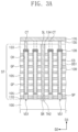
- FIG. 2 is a plan view illustrating a semiconductor memory device according to some embodiments of the inventive concept.
- FIGS. 3 A and 3 B are cross-sectional views taken along lines I-I′ and II-IF of FIG. 2 , respectively, to illustrate a semiconductor memory device according to some embodiments of the inventive concept.
- FIG. 4 is an enlarged view of a region ‘R’ of FIG. 3 B .
- a semiconductor memory device may include a cell array region CR and an extension region ER provided at an end portion of the cell array region CR.
- the extension regions ER may be provided at both end portions of the cell array region CR, respectively.
- the cell array region CR and the extension region ER will be described based on a substrate 100 .
- a plurality of stack structures ST may be disposed on a substrate 100 including the cell array region CR and the extension region ER.
- the stack structures ST may extend in a first direction D 1 parallel to a top surface of the substrate 100 and may be spaced apart from each other in a second direction D 2 , which is parallel to the top surface of the substrate 100 and is perpendicular to the first direction D 1 .
- the substrate 100 may include a silicon substrate, a silicon-germanium substrate, a germanium substrate, and/or a single-crystalline epitaxial layer grown on a single-crystalline silicon substrate.
- a source region SR (see, e.g., FIG. 3 B ) may be disposed in the substrate 100 .
- the source region SR may be disposed between the stack structures ST in a plan view and may extend in the first direction D 1 .
- the source region SR may be a dopant region having a different conductivity type from that of the substrate 100 .
- Each of the stack structures ST may include horizontal electrodes GP stacked in a third direction D 3 perpendicular to the top surface of the substrate 100 .
- a lowermost one of the horizontal electrodes GP may be the ground selection line GSL of FIG. 1
- an uppermost one of the horizontal electrodes GP may be the string selection line SSL of FIG. 1 .
- the horizontal electrodes GP between the lowermost and uppermost horizontal electrodes may be the word lines WL.
- a plurality of the horizontal electrodes GP may be used as the string selection lines SSL.
- the horizontal electrodes GP may include a doped semiconductor material (e.g., doped silicon), a metal (e.g., tungsten, copper, or aluminum), a conductive metal nitride (e.g., titanium nitride or tantalum nitride), and/or a transition metal (e.g., titanium or tantalum).
- a doped semiconductor material e.g., doped silicon
- a metal e.g., tungsten, copper, or aluminum
- a conductive metal nitride e.g., titanium nitride or tantalum nitride
- a transition metal e.g., titanium or tantalum
- Second horizontal insulating layers 105 may be disposed between the horizontal electrodes GP on the cell array region CR.
- First horizontal insulating layers 101 may be disposed between the horizontal electrodes GP on the extension region ER.
- the first horizontal insulating layers 101 and the horizontal electrodes GP may be alternately and repeatedly stacked on the extension region ER
- the second horizontal insulating layers 105 and the horizontal electrodes GP may be alternately and repeatedly stacked on the cell array region CR.
- the second horizontal insulating layers 105 may be connected to the first horizontal insulating layers 101 near a boundary between the cell array region CR and the extension region ER.
- the first and second horizontal insulating layers 101 and 105 may have different thicknesses in the D 3 direction in accordance with characteristics of the semiconductor memory device.
- the horizontal insulating layers 101 and 105 may include, for example, silicon oxide.
- a buffer layer 110 may be provided between the lowermost horizontal electrode GP and the substrate 100 .
- the buffer layer 110 may include silicon oxide.
- a first separation pattern 133 may be provided on the uppermost horizontal electrode GP on the cell array region CR.
- the first separation pattern 133 may include silicon oxide.
- End portions (i.e., pads) of the horizontal electrodes GP may be exposed (i.e., be free of other layers or materials) in a staircase shape on the extension region ER.
- Each of the pads may be defined as the end portion of each of the horizontal electrodes GP, which is exposed by another horizontal electrode GP disposed directly thereon.
- Contacts for applying voltages to the horizontal electrodes GP may be connected to the end portions (i.e., the pads) of the horizontal electrodes GP.
- a sidewall of an end portion of each of the first horizontal insulating layers 101 may be aligned with a sidewall of the end portion of the horizontal electrode GP disposed directly thereunder.
- a first interlayer insulating layer 131 may be provided to cover the pads on the extension region ER.
- a second interlayer insulating layer 132 may be provided on the first interlayer insulating layer 131 on the extension region ER.
- a top surface of the second interlayer insulating layer 132 may be located at the same level as a top surface of the first separation pattern 133 .
- the first and second interlayer insulating layers 131 and 132 may include silicon oxide.
- each of the horizontal electrodes GP may include a cell portion CG on the cell array region CR and an extension portion EG on the extension region ER. Some horizontal electrodes GP (e.g., the uppermost horizontal electrodes) may not include the extension portion EG.
- a top surface TS 2 of the extension portion EG may be located at a higher level in the D 3 direction than a top surface TS 1 of the cell portion CG.
- a bottom surface BS 2 of the extension portion EG may be located at a lower level in the D 3 direction than a bottom surface BS 1 of the cell portion CG.
- a thickness T 2 of the extension portion EG may be greater than a thickness T 1 of the cell portion CG. Due to the level difference and/or the thickness difference, the horizontal electrode GP may have a stepped structure at a boundary of the extension portion EG and the cell portion CG.
- Vertical structures VS 1 and VS 2 may be provided to penetrate the stack structure ST.
- the vertical structures VS 1 and VS 2 may be provided in vertical holes CH penetrating the stack structure ST.
- the vertical structures VS 1 and VS 2 may include first vertical structures VS 1 provided on the cell array region CR and second vertical structures VS 2 provided on the extension region ER.
- the first vertical structures VS 1 and the horizontal electrodes GP adjacent thereto may constitute the cell strings CSTR of FIG. 1 .
- the second vertical structures VS 2 may not constitute memory cell transistors, but may be dummy structures for supporting a mold structure in a manufacturing process.
- the second vertical structures VS 2 may not be connected to an upper interconnection line through contacts.
- the first vertical structures VS 1 may be arranged in a zigzag form in the second direction D 2 when viewed in a plan view.
- Each of the vertical structures VS 1 and VS 2 may include a filling layer 139 , a channel layer CS, a data storage layer DS 1 or DS 2 , and a pad pattern 128 .
- the channel layer CS and the data storage layer DS 1 or DS 2 may be sequentially stacked on a sidewall of the filling layer 139 .
- the channel layer CS may be disposed between the filling layer 139 and the data storage layer DS 1 or DS 2 .
- the pad pattern 128 may be disposed in an upper portion of each of the vertical structures VS 1 and VS 2 and may be on and at least partially cover a top surface of the data storage layer DS 1 or DS 2 .
- the channel layer CS may include a poly-crystalline silicon layer, an organic semiconductor layer, or a carbon nanostructure.
- Each of the data storage layers DS 1 and DS 2 may include a tunneling insulating layer TL, a charge storage layer CL, and a blocking insulating layer BL.
- the tunneling insulating layer TL may border a sidewall of the channel layer CS and may extend along the sidewall of the channel layer CS in the third direction D 3 .
- the tunneling insulating layer TL may include, for example, a silicon oxide layer.
- the charge storage layer CL may include a silicon nitride layer.
- the blocking insulating layer BL may include a silicon oxide layer.
- a first data storage layer DS 1 of the first vertical structure VS 1 and a second data storage layer DS 2 of the second vertical structure VS 2 may have different structures from each other.
- structures of the charge storage layer and the blocking insulating layer of the first data storage layer DS 1 may be different from those of the charge storage layer CL and the blocking insulating layer BL of the second data storage layer DS 2 .
- the charge storage layer CL of the second data storage layer DS 2 may continuously extend in the third direction D 3 along sidewalls of the horizontal electrodes GP and sidewalls of the first horizontal insulating layers 101 .
- the charge storage layer CL of the second data storage layer DS 2 may be provided in regions between the channel layer CS and the first horizontal insulating layers 101 and regions between the channel layer CS and the horizontal electrodes GP.
- the charge storage layer of the first data storage layer DS 1 may include charge storage patterns CP that are spaced apart from each other in the third direction D 3 with the second horizontal insulating layers 105 interposed therebetween.
- the charge storage patterns CP of the first data storage layer DS 1 may be intermittently disposed along the third direction D 3 .
- Each of the charge storage patterns CP may have a ring shape when viewed in a plan view.
- the charge storage patterns CP may be disposed in regions between the channel layer CS and the horizontal electrodes GP, but may not be disposed in regions between the channel layer CS and the second horizontal insulating layers 105 . Thus, charges included in each of the charge storage patterns CP may not move or spread into other charge storage patterns CP. Data retention characteristics of the semiconductor memory device may be improved due to the structure in which the charge storage patterns CP are vertically separated from each other.
- the structure of the blocking insulating layer of the first data storage layer DS 1 may be different from that of the blocking insulating layer BL of the second data storage layer DS 2 .
- the blocking insulating layer BL of the second data storage layer DS 2 may continuously extend in the third direction D 3 along the sidewalls of the horizontal electrodes GP and the sidewalls of the first horizontal insulating layers 101 .
- the blocking insulating layer of the first data storage layer DS 1 may include blocking insulating patterns BP that are spaced apart from each other in the third direction D 3 with the second horizontal insulating layers 105 interposed therebetween.
- Each of the blocking insulating patterns BP may have a ring shape when viewed in a plan view.
- a width T 3 , in the third direction D 3 , of each of the blocking insulating patterns BP may be greater than the thickness T 1 of an adjacent portion (i.e., the cell portion CG) of the horizontal electrode GP.
- a width T 3 , in the third direction D 3 , of each of the charge storage patterns CP may be greater than the thickness T 1 of an adjacent portion (i.e., the cell portion CG) of the horizontal electrode GP.
- the tunneling insulating layer TL of the first data storage layer DS 1 may have substantially the same shape as the tunneling insulating layer TL of the second data storage layer DS 2 .
- the structure of the tunneling insulating layer TL of the first data storage layer DS 1 may be different from that of the tunneling insulating layer TL of the second data storage layer DS 2 .
- the tunneling insulating layer of the first data storage layer DS 1 may include tunneling insulating patterns TP spaced apart from each other in the third direction D 3 .
- Semiconductor pillars SP may be disposed between the substrate 100 and the vertical structures VS 1 and VS 2 .
- the semiconductor pillars SP may be formed by performing a selective epitaxial growth (SEG) process using the substrate 100 as a seed.
- the semiconductor pillars SP may include an intrinsic semiconductor material or a P-type semiconductor material.
- a barrier insulating layer 160 may be disposed between the horizontal electrodes GP and the horizontal insulating layers 105 and 101 and may extend between the blocking insulating layer BL and the horizontal electrodes GP.
- the barrier insulating layer 160 may be in physical contact with the blocking insulating layer BL.
- the barrier insulating layer 160 may include a single layer or a plurality of layers.
- the barrier insulating layer 160 may include a metal oxide layer and/or a metal nitride layer.
- the barrier insulating layer 160 may be a portion of a blocking insulating layer of a charge trap-type non-volatile memory transistor.
- the pad pattern 128 may be in physical contact with the channel layer CS and may be electrically connected to the channel layer CS.
- the pad pattern 128 may include poly-crystalline silicon doped with dopants of which a conductivity type is different from that of dopants (e.g., P-type dopants) of the substrate 100 .
- the pad pattern 128 may include N-type dopants.
- a source line SL may be disposed between the stack structures ST and may be connected to the source region SR.
- the source line SL may have a line shape or rectangular shape extending along the source region SR in the first direction D 1 when viewed in a plan view (see, e.g., FIG. 2 ).
- the source line SL may include contacts separated from each other in the first direction D 1 .
- the source line SL may be formed of a metal (e.g., tungsten, copper, or aluminum) and/or a transition metal (e.g., titanium or tantalum).
- a second separation pattern 134 may be disposed between the source line SL and the stack structures ST.
- the second separation pattern 134 may extend in the first direction D 1 .
- the second separation pattern 134 may include an insulating material (e.g., silicon oxide or silicon nitride).
- FIG. 5 is an enlarged view of a region ‘S’ of FIG. 2 to illustrate a level of one of horizontal electrodes.
- a second trench TH 2 may be provided between the stack structures ST adjacent to each other, and the source line SL and the second separation pattern 134 may be provided in the second trench TH 2 .
- the second separation pattern 134 may be provided on the cell array region CR and the extension region ER.
- a protrusion separation pattern 138 may protrude from the second separation pattern 134 toward the horizontal electrode GP in the second direction D 2 and/or a direction opposite to the second direction D 2 .
- the protrusion separation pattern 138 may be provided in a first trench TH 1 .
- the protrusion separation pattern 138 may be a portion of a layer formed simultaneously and/or in synchronization with the first separation pattern 133 .
- the first trench TH 1 and the second trench TH 2 may expose the top surface of the substrate 100 .
- the protrusion separation pattern 138 may be provided locally on the cell array region CR, but may not extend onto the extension region ER.
- the first and second separation patterns 133 and 134 may include silicon oxide.
- a third interlayer insulating layer 135 may be provided to be on and at least partially cover the second interlayer insulating layer 132 and the first separation pattern 133 .
- the third interlayer insulating layer 135 may include at least one of a silicon oxide layer, a silicon nitride layer, and/or a silicon oxynitride layer.
- Contact plugs CT may penetrate the third interlayer insulating layer 135 and may be in contact with the pad patterns 128 .
- the contact plugs CT may include doped silicon and/or a metallic material (e.g., tungsten (W), copper (Cu), or aluminum (Al)).
- Bit lines 176 may be disposed on the third interlayer insulating layer 135 .
- the bit lines 176 may be electrically connected to the first vertical structures VS 1 through the contact plugs CT.
- the bit lines 176 may include a conductive material.
- FIGS. 6 , 8 and 15 are plan views illustrating a method of manufacturing a semiconductor memory device according to some embodiments of the inventive concept.
- FIGS. 7 A, 9 A, 10 A, 12 A, 14 A and 16 A are cross-sectional views taken along lines I-I′ of FIGS. 6 , 8 and 15 .
- FIGS. 7 B, 9 B, 10 B, 12 B, 14 B and 16 B are cross-sectional views taken along lines II-IF of FIGS. 6 , 8 and 15 .
- FIGS. 11 , 13 A, 13 B and 13 C are enlarged views of regions ‘R’ of FIGS. 10 B and 12 B .
- FIG. 17 is an enlarged view of a region ‘S’ of FIG. 15 .
- a mold structure MS may be formed on a substrate 100 including a cell array region CR and an extension region ER.
- the mold structure MS may include first layers and second layers, which are alternately and repeatedly stacked on the substrate 100 .
- the first layers may be first horizontal insulating layers 101
- the second layers may be sacrificial layers 102 .
- the first horizontal insulating layers 101 may include a material having an etch selectivity with respect to the sacrificial layers 102 .
- the first horizontal insulating layers 101 may be silicon oxide layers
- the sacrificial layers 102 may be silicon nitride layers.
- a buffer layer 110 may be formed at a bottom of the mold structure MS.
- the buffer layer 110 may be a silicon oxide layer.
- the mold structure MS may be patterned to form a staircase structure on the extension region ER.
- the staircase structure may be formed by processes of forming a mask pattern and etching processes.
- a first interlayer insulating layer 131 on and at least partially covering the staircase structure may be formed.
- Vertical holes CH may be formed to penetrate the mold structure MS.
- the vertical holes CH may expose the substrate 100 , i.e., portions of the substrate 100 may be free of the mold structure MS.
- the vertical holes CH may be formed using an anisotropic etching process.
- a mask pattern may be formed on the mold structure MS, and the vertical holes CH may be formed by etching the mold structure MS exposed by the mask pattern.
- the etching process for forming the vertical holes CH may be performed until portions of the top surface of the substrate 100 are exposed, i.e., are free of the mold structure.
- the top surface of the substrate 100 may be recessed by over-etching of the etching process.
- the vertical holes CH may be formed on both the cell array region CR and the extension region ER.
- Semiconductor pillars SP may be formed or grown from the top surface of the substrate 100 exposed by the vertical holes CH.
- the semiconductor pillars SP may include an intrinsic semiconductor material or a P-type semiconductor material. In some embodiments, the semiconductor pillars SP may be omitted.
- Vertical structures VS 1 and VS 2 may be formed on the semiconductor pillars SP in the vertical holes CH.
- First vertical structures VS 1 on the cell array region CR and second vertical structures VS 2 on the extension region ER may be formed to have substantially the same layers and the same shape.
- Each of the vertical structures VS 1 and VS 2 may include a filling layer 139 , a channel layer CS, a data storage layer DS, and a pad pattern 128 .
- the channel layer CS may penetrate the data storage layer DS so as to be connected to the semiconductor pillar SP.
- the data storage layer DS may be formed on inner surfaces of the vertical holes CH.
- lower portions of the data storage layer DS may be etched by a dry etching process to expose top surfaces of the semiconductor pillars SP, i.e., top surfaces of the semiconductor pillars SP may be free of the data storage layer DS.
- the channel layer CS may be formed on sidewalls of the data storage layer DS. Lower portions of the channel layer CS may be connected to the semiconductor pillars SP.
- the filling layer 139 on and at least partially covering sidewalls of the channel layer CS may be formed in the vertical holes CH.
- the filling layer 139 may be formed using, for example, a spin-on-glass (SOG) technique.
- the filling layer 139 may include an insulating material, e.g., a silicon oxide layer or a silicon nitride layer. Upper portions of the data storage layer DS, the channel layer CS and the filling layer 139 may be removed to form empty regions in the vertical holes CH, and then, the pad patterns 128 may be formed in the empty regions with a conductive material.
- a second interlayer insulating layer 132 on and at least partially covering the vertical structures VS 1 and VS 2 may be formed.
- the second interlayer insulating layer 132 may include silicon oxide.
- first trenches TH 1 may be formed to penetrate the mold structure MS.
- the first trenches TH 1 may expose, e.g., provide access to the top surface of the substrate 100 .
- the first trenches TH 1 may be formed using an ion beam etching process.
- the first trenches TH 1 may be formed on the cell array region CA, and both end portions of each of the first trenches TH 1 may be provided in the cell array region CR when viewed in a plan view (see, e.g., FIG. 8 ).
- the first trenches TH 1 may extend in the first direction D 1 and may be spaced apart from each other in the second direction D 2 .
- the first horizontal insulating layers 101 exposed or revealed by the first trenches TH 1 may be removed from the cell array region CR.
- the first horizontal insulating layers 101 of the cell array region CR may be removed using an isotropic etching process.
- the first horizontal insulating layers 101 may be removed using an etch recipe (e.g., hydrofluoric acid (HF)) having an etch selectivity with respect to the sacrificial layers 102 .
- etch recipe e.g., hydrofluoric acid (HF)
- First gap regions GR 1 that expose the data storage layer DS between the sacrificial layers 102 and are connected to the first trenches TH 1 may be formed by the removal of the first horizontal insulating layers 101 of the cell array region CR.
- first trenches TH 1 are confined on the cell array region CR and are not formed on the extension region ER, it is possible to reduce or minimize loss or damage of the second interlayer insulating layer 132 and the first interlayer insulating layer 131 on the extension region ER. As a result, processes of manufacturing the semiconductor memory device may be simplified and dispersion of a subsequent process of forming horizontal electrodes may be reduced.
- FIG. 11 is an enlarged view of a region ‘R’ of FIG. 10 B .
- the first gap regions GR 1 may be locally formed on the cell array region CR.
- the first horizontal insulating layers 101 may be on and at least partially cover the data storage layers DS of the second vertical structures VS 2 disposed on the extension region ER.
- FIGS. 12 A and 12 B an etching process may be performed on the data storage layer DS (hereinafter, referred to as a first data storage layer DS 1 ) of the first vertical structure VS 1 .
- FIGS. 13 A, 13 B and 13 C are enlarged views of a region ‘R’ of FIG. 12 B .
- the blocking insulating layer of the first data storage layer DS 1 may be etched to form blocking insulating patterns BP separated from each other in the third direction D 3 .
- the blocking insulating layer BL of the data storage layer DS (hereinafter, referred to as a second data storage layer DS 2 ) of the second vertical structure VS 2 may be at least partially covered by the first horizontal insulating layers 101 and thus may not be etched.
- the etching process for forming the blocking insulating patterns BP may be performed using an etch recipe (e.g., hydrofluoric acid (HF)) having an etch selectivity with respect to the sacrificial layers 102 and the charge storage layer CL.
- etch recipe e.g., hydrofluoric acid (HF)
- etching of the sacrificial layers 102 and the charge storage layer CL may be reduced or minimized during the formation of the blocking insulating patterns BP.
- Portions of the sacrificial layers 102 which are exposed by the first gap regions GR 1 , may have substantially the same thickness (e.g., a first thickness T 6 ) as portions of the sacrificial layers 102 , which are covered by the first horizontal insulating layers 101 .
- Portions of the first horizontal insulating layers 101 exposed by the first gap regions GR 1 and a portion of the second interlayer insulating layer 132 on the extension region ER may also be removed.
- a top surface of the second interlayer insulating layer 132 may be lower in the D 3 direction than that of the second interlayer insulating layer 132 of FIG. 10 B .
- the charge storage layer CL exposed between the blocking insulating patterns BP of the first data storage layer DS 1 may be etched to form charge storage patterns CP separated from each other in the third direction D 3 .
- the charge storage layer CL of the second data storage layer DS 2 of the second vertical structure VS 2 may be at least partially covered by the first horizontal insulating layers 101 and, thus, may not be etched.
- the etching process for forming the charge storage patterns CP may be performed using an etch recipe (e.g., phosphoric acid (H 3 PO 4 )) having an etch selectivity with respect to the blocking insulating patterns BP and the tunneling insulating layer TL.
- an etch recipe e.g., phosphoric acid (H 3 PO 4 )
- a difference in etch rate between the charge storage layer CL and the sacrificial layers 102 may be less than a difference in etch rate between the charge storage layer CL and the blocking insulating patterns BP (and the tunneling insulating layer TL).
- top and bottom surfaces of the portions of the sacrificial layers 102 exposed or revealed by the first gap regions GR 1 may be etched while the charge storage layer CL is etched, and, thus, the etched portions of the sacrificial layers 102 may have a second thickness T 7 less than the first thickness T 6 .
- the first thickness T 6 of the portions of the sacrificial layers 102 at least partially covered by the first horizontal insulating layers 101 may be maintained.
- stepped structures may be formed at the tops and bottoms of the sacrificial layers 102 .
- the tunneling insulating layer TL exposed or revealed between the charge storage patterns CP of the first data storage layer DS 1 may be etched to form tunneling insulating patterns TP separated from each other in the third direction D 3 .
- the tunneling insulating layer TL of the second data storage layer DS 2 of the second vertical structure VS 2 may be at least partially covered by the first horizontal insulating layers 101 and, thus, may not be etched.
- a gap-fill insulating layer (hereinafter, referred to as a first separation pattern) 133 may be formed to fill the first trenches TH 1 and the first gap regions GR 1 extending from the first trenches TH 1 .
- portions of the first separation pattern 133 which are in the first gap regions GR 1 may be referred to as second horizontal insulating layers 105 .
- the first separation pattern 133 may include silicon oxide.
- second trenches TH 2 may be formed to penetrate the mold structure MS.
- the second trenches TH 2 may expose the top surface of the substrate 100 , i.e., at least portions of the top surface of the substrate are free of the mold structure MS.
- the second trenches TH 2 may be formed using an ion beam etching process.
- Each of the second trenches TH 2 may be formed on the cell array region CR and the extension region ER. In other words, each of the second trenches TH 2 may intersect the cell array region CR and the extension region ER.
- the second trenches TH 2 may extend in the first direction D 1 and may be spaced apart from each other in the second direction D 2 .
- the second trenches TH 2 may overlap with the first trenches TH 1 , respectively.
- a portion of sidewalls of the second trenches TH 2 may not be aligned with the first trenches TH 1 , and, thus, a portion of the first trench TH 1 and a protrusion separation pattern 138 in the portion of the first trench TH 1 may remain.
- the protrusion separation pattern 138 corresponding to a portion of a remaining first separation pattern 133 may be in contact with sidewalls of the sacrificial layers 102 between the second horizontal insulating layers 105 .
- the sacrificial layers 102 exposed or revealed through the second trenches TH 2 may be replaced with horizontal electrodes GP.
- the sacrificial layers 102 exposed through the second trenches TH 2 may be selectively removed to form second gap regions, and the horizontal electrodes GP may be formed in the second gap regions, respectively.
- the formation of the horizontal electrodes GP may include forming a conductive layer in the second gap regions, and performing an etching process on the conductive layer to remove the conductive layer formed in the second trenches TH 2 and to locally leave portions of the conductive layer in the second gap regions, respectively.
- a process of forming the barrier insulating layer 160 illustrated in FIG. 4 may be performed before the formation of the horizontal electrodes GP.
- the barrier insulating layer 160 may be formed on to at least partially conformally cover top surfaces and bottom surfaces of the second horizontal insulating layers 105 exposed or revealed by the second gap regions.
- the barrier insulating layer 160 may include a single layer or a plurality of layers.
- the barrier insulating layer 160 may be a portion of a blocking insulating layer of a charge trap-type non-volatile memory transistor.
- the barrier insulating layer 160 may be a dielectric layer (e.g., a high-k material such as aluminum oxide (Al 2 O 3 ), hafnium oxide (HfO 2 ), zirconium oxide (ZrO 2 ), hafnium-aluminum oxide (HfAlO), and/or hafnium-silicon oxide (HfSiO)).
- Stack structures ST including the horizontal electrodes GP and the horizontal insulating layers 105 and 101 may be formed by the formation of the horizontal electrodes GP.
- source regions SR may be formed in the substrate 100 exposed or revealed through the second trenches TH 2 .
- the source region SR may be formed using an ion implantation process.
- the source region SR may have a different conductivity type from that of the substrate 100 .
- a second separation pattern 134 and a source line SL may be sequentially formed in each of the second trenches TH 2 .
- the second separation patterns 134 may be formed on and at least partially cover sidewalls of the second trenches TH 2 .
- the formation of the second separation patterns 134 may include forming an insulating layer (not shown) on and at least partially covering the sidewalls and bottom surfaces of the second trenches TH 2 , and etching portions of the insulating layer (not shown), which are on and at least partially cover the bottom surfaces of the second trenches TH 2 , to expose or reveal the top surface of the substrate 100 , i.e., portions of the top surface of the substrate may be free of insulating layer.
- the second separation patterns 134 may be formed of, for example, silicon oxide or silicon nitride.
- the source line SL may be in each of the second trenches TH 2 in which the second separation patterns 134 are formed.
- the source line SL may be formed using, for example, a chemical vapor deposition (CVD) process, a physical vapor deposition (PVD) process, and/or an atomic layer deposition (ALD) process.
- CVD chemical vapor deposition
- PVD physical vapor deposition
- ALD atomic layer deposition
- the source line SL may be formed of a metal (e.g., tungsten, copper, and/or aluminum) and/or a transition metal (e.g., titanium and/or tantalum).
- a third interlayer insulating layer 135 may be formed after the formation of the source line SL.
- the third interlayer insulating layer 135 may be on and at least partially cover the top surface of the first separation pattern 133 and the top surface of the second interlayer insulating layer 132 .
- the third interlayer insulating layer 135 may include an insulating material, such as a silicon oxide layer, a silicon nitride layer, and/or a silicon oxynitride layer.
- Contact plugs CT may be formed to penetrate the third interlayer insulating layer 135 .
- the contact plugs CT may be in physical contact with the pad patterns 128 .
- the contact plugs CT may include doped silicon and/or a conductive material (e.g., tungsten (W), copper (Cu), and/or aluminum (Al)).
- Bit lines 176 being in physical contact with the contact plugs CT may be formed on the third interlayer insulating layer 135 .
- the bit lines 176 may intersect the stack structures ST, and each of the bit lines 176 may be connected to the first vertical structures VS 1 arranged in the second direction D 2 .
- the bit lines 176 may include a conductive material (e.g., tungsten (W), aluminum (Al), and/or copper (Cu)).
- FIGS. 18 A and 18 B are cross-sectional views taken along the lines I-I′ and II-IF of FIG. 2 , respectively, to illustrate a semiconductor memory device according to some embodiments of the inventive concept.
- FIG. 19 is an enlarged view of a region ‘R’ of FIG. 18 B .
- a semiconductor memory device may include protective semiconductor patterns 166 provided on sidewalls of the second vertical structures VS 2 .
- the protective semiconductor patterns 166 may be provided locally on the extension region ER but may not be provided on sidewalls of the first vertical structures VS 1 disposed on the cell array region CR.
- the protective semiconductor patterns 166 may be spaced apart from each other with the horizontal electrodes GP interposed therebetween. In other words, the protective semiconductor patterns 166 disposed on the sidewall of one of the second vertical structures VS 2 may be separated from each other by the horizontal electrodes GP.
- each of the protective semiconductor patterns 166 separated from each other by the horizontal electrodes GP may have a ring shape when viewed in a plan view.
- the protective semiconductor patterns 166 may be provided between the blocking insulating layer BL of the second data storage layer DS 2 and the first horizontal insulating layers 101 .
- the protective semiconductor patterns 166 may include a semiconductor material, such as poly-crystalline silicon.
- FIGS. 20 A and 21 A are cross-sectional views taken along the line I-I′ of FIG. 2 to illustrate a method of manufacturing a semiconductor memory device, according to some embodiments of the inventive concept.
- FIGS. 20 B and 21 B are cross-sectional views taken along the line II-IF of FIG. 2 to illustrate a method of manufacturing a semiconductor memory device, according to some embodiments of the inventive concept.
- FIGS. 22 A and 22 B are enlarged views corresponding to FIGS. 11 and 13 B , respectively.
- the mold structure MS including the first horizontal insulating layers 101 and the sacrificial layers 102 , which are alternately and repeatedly stacked, may be provided on the substrate 100 .
- the mold structure MS may include the staircase structure on the extension region ER.
- the first interlayer insulating layer 131 on and at least partially covering the staircase structure may be provided.
- portions of the first horizontal insulating layers 101 exposed or revealed by the vertical holes CH may be removed to form recess regions RS on the cell array region CR and the extension region ER.
- Each of the recess regions RS may be a region defined by adjacent sacrificial layers 102 and a sidewall of the first horizontal insulating layer 101 between the adjacent sacrificial layers 102 .
- the recess regions RS may be formed using an etch recipe (e.g., hydrofluoric acid (HF)) having an etch selectivity with respect to the sacrificial layers 102 .
- the first interlayer insulating layer 131 may be etched together with the first horizontal insulating layers 101 .
- a protective semiconductor layer 165 in the recess regions RS may be formed in the vertical holes CH.
- the protective semiconductor layer 165 may be formed of a material having an etch selectivity with respect to the first horizontal insulating layers 101 and the sacrificial layers 102 .
- the protective semiconductor layer 165 may be a poly-silicon layer.
- the protective semiconductor layer 165 may have a bent or uneven inner surface due to the recess regions RS.
- a process of trimming the protective semiconductor layer 165 may be performed to form separated protective semiconductor patterns 166 in the recess regions RS, respectively.
- the trimming process may include a wet etching process.
- the semiconductor pillars SP and the vertical structures VS 1 and VS 2 may be formed in the vertical holes CH as described with reference to FIGS. 6 , 7 A and 7 B .
- FIG. 22 A is an enlarged view of a region corresponding to FIG. 11 to illustrate a structure obtained by performing the example processes described with reference to FIGS. 8 , 9 A, 9 B, 10 A and 10 B on the resultant structure of FIGS. 21 A and 21 B .
- the data storage layer DS on the cell array region CR may be protected by the protective semiconductor patterns 166 while the first horizontal insulating layers 101 exposed or revealed by the first trenches TH 1 are removed from the cell array region CR. As a result, damage to the data storage layer DS on the cell array region CR may be reduced or prevented.
- FIG. 22 B is an enlarged view of a region corresponding to FIG. 13 B to illustrate a structure obtained by performing the example processes described with reference to FIGS. 12 A, 12 B, 13 A and 13 B on the resultant structure of FIG. 22 A .
- the protective semiconductor patterns 166 on the cell array region CR may be removed by the processes described with reference to FIGS. 12 A, 12 B, 13 A and 13 B , but the protective semiconductor patterns 166 on the extension region ER may be at least partially covered by the first horizontal insulating layers 101 and the interlayer insulating layers 131 and 132 and, thus, may remain.
- the semiconductor memory device may include the protective semiconductor patterns 166 provided on the sidewalls of the second vertical structures VS 2 .
- the example processes of FIGS. 14 A, 14 B, 16 A and 16 B may be performed to manufacture the semiconductor memory device according to the embodiments described with reference to FIGS. 18 A and 18 B .
- FIG. 23 is a cross-sectional view taken along the line II-IF of FIG. 2 to illustrate a semiconductor memory device according to some embodiments of the inventive concept.
- a semiconductor memory device may include a peripheral circuit structure PS and a cell array structure CS disposed on the peripheral circuit structure PS.
- the cell array structure CS may overlap the peripheral circuit structure PS when viewed in a plan view.
- the peripheral circuit structure PS may include peripheral logic circuits PTR integrated on a semiconductor substrate 1 and a lower interlayer insulating layer 50 on and at least partially covering the peripheral logic circuits PTR.
- the semiconductor substrate 1 may include a silicon substrate, a silicon-germanium substrate, a germanium substrate, and/or a single-crystalline epitaxial layer grown on a single-crystalline silicon substrate.
- the semiconductor substrate 1 may include active regions defined by a device isolation layer 11 .
- the peripheral logic circuits PTR may include row and column decoders, a page buffer, and control circuits and may include NMOS and PMOS transistors, low-voltage and high-voltage transistors and a resistor, which are integrated on the semiconductor substrate 1 .
- Peripheral circuit interconnection lines 33 may be electrically connected to the peripheral logic circuits PTR through peripheral contact plugs 31 .
- the peripheral contact plugs 31 and the peripheral circuit interconnection lines 33 may be connected to the NMOS and PMOS transistors.
- the lower interlayer insulating layer 50 may be on and at least partially cover peripheral gate electrodes, the peripheral contact plugs 31 , and the peripheral circuit interconnection lines 33 .
- the lower interlayer insulating layer 50 may include a plurality of stacked insulating layers.
- the lower interlayer insulating layer 50 may include a silicon oxide layer, a silicon nitride layer, a silicon oxynitride layer, and/or a low-k dielectric layer.
- An etch stop layer 60 and a middle interlayer insulating layer 65 may be sequentially stacked on the lower interlayer insulating layer 50 .
- the etch stop layer 60 may be formed of an insulating material having an etch selectivity with respect to the lower interlayer insulating layer 50 .
- the etch stop layer 60 may include a silicon nitride layer and/or a silicon oxynitride layer.
- the middle interlayer insulating layer 65 may include the same material as the lower interlayer insulating layer 50 .
- the cell array structure CS may include a stack structure ST on a base layer 100 a .
- the base layer 100 a may be formed of a semiconductor material.
- the base layer 100 a may include silicon (Si), germanium (Ge), silicon-germanium (SiGe), gallium-arsenic (GaAs), indium-gallium-arsenic (InGaAs), or aluminum-gallium-arsenic (AlGaAs), or any mixture thereof.
- the base layer 100 a may be formed of a poly-silicon layer doped with N-type dopants.
- a region ‘R’ of FIG. 23 may be similar to FIG. 4 or 19 . Except that the stack structure ST includes a third horizontal insulating layer 99 , other components of the stack structure ST may be the same or similar as those described in the above embodiments.
- the third horizontal insulating layer 99 may be provided on the extension region, but may not be provided on the cell array region.
- a distance between a pair of the horizontal electrodes GP spaced apart from each other with the third horizontal insulating layer 99 interposed therebetween may be greater than a distance between other horizontal electrodes GP adjacent to each other.
- the stack structure ST may include a first stack structure and a second stack structure, which are spaced apart from each other with the third horizontal insulating layer 99 interposed therebetween.
- Each of the vertical structures VS 1 and VS 2 may have a stepped structure at a level adjacent to the third horizontal insulating layer 99 .
- the stepped structure may be generated because vertical holes in which the vertical structures VS 1 and VS 2 are provided are formed by a plurality of patterning processes of etching a first mold structure and a second mold structure, respectively.
- the charge storage patterns may be separated from each other in a direction perpendicular to the top surface of the substrate. Thus, charges included in each of the charge storage patterns may not move or spread into other charge storage patterns or the move or spread of the charges may be reduced.
- loss or damage of the interlayer insulating layer on the extension region may be reduced or minimized.
Abstract
Description
Claims (18)
Applications Claiming Priority (2)
| Application Number | Priority Date | Filing Date | Title |
|---|---|---|---|
| KR10-2019-0116373 | 2019-09-20 | ||
| KR1020190116373A KR20210034749A (en) | 2019-09-20 | 2019-09-20 | Semiconductor memory device and method of forming the same |
Publications (2)
| Publication Number | Publication Date |
|---|---|
| US20210091104A1 US20210091104A1 (en) | 2021-03-25 |
| US11653493B2 true US11653493B2 (en) | 2023-05-16 |
Family
ID=74882092
Family Applications (1)
| Application Number | Title | Priority Date | Filing Date |
|---|---|---|---|
| US16/874,159 Active 2041-01-11 US11653493B2 (en) | 2019-09-20 | 2020-05-14 | Semiconductor memory device and method of manufacturing the same |
Country Status (3)
| Country | Link |
|---|---|
| US (1) | US11653493B2 (en) |
| KR (1) | KR20210034749A (en) |
| CN (1) | CN112542467A (en) |
Citations (13)
| Publication number | Priority date | Publication date | Assignee | Title |
|---|---|---|---|---|
| US20140106569A1 (en) * | 2012-10-16 | 2014-04-17 | Jung-Ik Oh | Method of fabricating three-dimensional semiconductor device and three-dimensional semiconductor device fabricated using the same |
| US8796757B2 (en) | 2010-06-15 | 2014-08-05 | Kabushiki Kaisha Toshiba | Semiconductor memory device and method of manufacturing the same |
| US9865616B2 (en) | 2016-02-09 | 2018-01-09 | Toshiba Memory Corporation | Semiconductor memory device and method for manufacturing same |
| US20180053779A1 (en) * | 2016-08-19 | 2018-02-22 | SK Hynix Inc. | Manufacturing method of semiconductor device |
| US20180053781A1 (en) | 2015-10-06 | 2018-02-22 | Toshiba Memory Corporation | Semiconductor device and method for manufacturing same |
| US9911750B2 (en) | 2010-06-24 | 2018-03-06 | Samsung Electronics Co., Ltd. | Semiconductor memory devices including asymmetric word line pads |
| US10134750B2 (en) | 2014-12-30 | 2018-11-20 | Toshiba Memory Corporation | Stacked type semiconductor memory device and method for manufacturing the same |
| US20190080764A1 (en) | 2017-09-08 | 2019-03-14 | Toshiba Memory Corporation | Memory device |
| US20190081059A1 (en) | 2017-03-07 | 2019-03-14 | Yangtze Memory Technologies Co., Ltd. | Trench structures for three-dimensional memory devices |
| US10262936B2 (en) | 2017-02-08 | 2019-04-16 | Toshiba Memory Corporation | Semiconductor device and manufacturing method thereof |
| US10290651B2 (en) | 2012-11-14 | 2019-05-14 | SK Hynix Inc. | Semiconductor devices with non-overlapping slits in-between memory blocks |
| US10700090B1 (en) * | 2019-02-18 | 2020-06-30 | Sandisk Technologies Llc | Three-dimensional flat NAND memory device having curved memory elements and methods of making the same |
| US20200388627A1 (en) * | 2019-06-06 | 2020-12-10 | Micron Technology, Inc. | Integrated Assemblies Having Vertically-Spaced Channel Material Segments, and Methods of Forming Integrated Assemblies |
-
2019
- 2019-09-20 KR KR1020190116373A patent/KR20210034749A/en not_active Application Discontinuation
-
2020
- 2020-05-14 US US16/874,159 patent/US11653493B2/en active Active
- 2020-09-18 CN CN202010984502.8A patent/CN112542467A/en active Pending
Patent Citations (13)
| Publication number | Priority date | Publication date | Assignee | Title |
|---|---|---|---|---|
| US8796757B2 (en) | 2010-06-15 | 2014-08-05 | Kabushiki Kaisha Toshiba | Semiconductor memory device and method of manufacturing the same |
| US9911750B2 (en) | 2010-06-24 | 2018-03-06 | Samsung Electronics Co., Ltd. | Semiconductor memory devices including asymmetric word line pads |
| US20140106569A1 (en) * | 2012-10-16 | 2014-04-17 | Jung-Ik Oh | Method of fabricating three-dimensional semiconductor device and three-dimensional semiconductor device fabricated using the same |
| US10290651B2 (en) | 2012-11-14 | 2019-05-14 | SK Hynix Inc. | Semiconductor devices with non-overlapping slits in-between memory blocks |
| US10134750B2 (en) | 2014-12-30 | 2018-11-20 | Toshiba Memory Corporation | Stacked type semiconductor memory device and method for manufacturing the same |
| US20180053781A1 (en) | 2015-10-06 | 2018-02-22 | Toshiba Memory Corporation | Semiconductor device and method for manufacturing same |
| US9865616B2 (en) | 2016-02-09 | 2018-01-09 | Toshiba Memory Corporation | Semiconductor memory device and method for manufacturing same |
| US20180053779A1 (en) * | 2016-08-19 | 2018-02-22 | SK Hynix Inc. | Manufacturing method of semiconductor device |
| US10262936B2 (en) | 2017-02-08 | 2019-04-16 | Toshiba Memory Corporation | Semiconductor device and manufacturing method thereof |
| US20190081059A1 (en) | 2017-03-07 | 2019-03-14 | Yangtze Memory Technologies Co., Ltd. | Trench structures for three-dimensional memory devices |
| US20190080764A1 (en) | 2017-09-08 | 2019-03-14 | Toshiba Memory Corporation | Memory device |
| US10700090B1 (en) * | 2019-02-18 | 2020-06-30 | Sandisk Technologies Llc | Three-dimensional flat NAND memory device having curved memory elements and methods of making the same |
| US20200388627A1 (en) * | 2019-06-06 | 2020-12-10 | Micron Technology, Inc. | Integrated Assemblies Having Vertically-Spaced Channel Material Segments, and Methods of Forming Integrated Assemblies |
Also Published As
| Publication number | Publication date |
|---|---|
| CN112542467A (en) | 2021-03-23 |
| US20210091104A1 (en) | 2021-03-25 |
| KR20210034749A (en) | 2021-03-31 |
Similar Documents
| Publication | Publication Date | Title |
|---|---|---|
| US10854622B2 (en) | Vertical memory devices and methods of manufacturing the same | |
| US10453859B2 (en) | Methods of manufacturing vertical memory devices | |
| CN109427804B (en) | Three-dimensional semiconductor device | |
| US11696442B2 (en) | Vertical memory devices and methods of manufacturing the same | |
| US11211402B2 (en) | Three-dimensional semiconductor memory device | |
| US10177164B2 (en) | Semiconductor device | |
| US11785768B2 (en) | Three-dimensional semiconductor memory devices | |
| KR102054226B1 (en) | Semiconductor device and method of manufacturing the same | |
| US10515979B2 (en) | Three-dimensional semiconductor devices with inclined gate electrodes | |
| US11069709B2 (en) | Vertical memory devices | |
| KR20140025864A (en) | A vertical type semiconductor device and method of manufacturing the same | |
| US10861877B2 (en) | Vertical memory devices | |
| JP6004215B2 (en) | Self-aligned method of forming a semiconductor memory array of floating gate memory cells having a single poly layer | |
| KR20200141150A (en) | Vertical memory devices | |
| KR102640872B1 (en) | Three dimensional semiconductor device | |
| US11653493B2 (en) | Semiconductor memory device and method of manufacturing the same | |
| US20190378850A1 (en) | Vertical memory devices | |
| US11737273B2 (en) | Three-dimensional semiconductor memory devices |
Legal Events
| Date | Code | Title | Description |
|---|---|---|---|
| AS | Assignment |
Owner name: SAMSUNG ELECTRONICS CO., LTD., KOREA, REPUBLIC OF Free format text: ASSIGNMENT OF ASSIGNORS INTEREST;ASSIGNORS:JEONG, SANGHOON;HONG, SANGJUN;SHIM, SUNIL;AND OTHERS;SIGNING DATES FROM 20200406 TO 20200414;REEL/FRAME:052665/0068 |
|
| FEPP | Fee payment procedure |
Free format text: ENTITY STATUS SET TO UNDISCOUNTED (ORIGINAL EVENT CODE: BIG.); ENTITY STATUS OF PATENT OWNER: LARGE ENTITY |
|
| STPP | Information on status: patent application and granting procedure in general |
Free format text: APPLICATION DISPATCHED FROM PREEXAM, NOT YET DOCKETED |
|
| STPP | Information on status: patent application and granting procedure in general |
Free format text: DOCKETED NEW CASE - READY FOR EXAMINATION |
|
| STPP | Information on status: patent application and granting procedure in general |
Free format text: NON FINAL ACTION MAILED |
|
| STPP | Information on status: patent application and granting procedure in general |
Free format text: RESPONSE TO NON-FINAL OFFICE ACTION ENTERED AND FORWARDED TO EXAMINER |
|
| STPP | Information on status: patent application and granting procedure in general |
Free format text: FINAL REJECTION MAILED |
|
| STPP | Information on status: patent application and granting procedure in general |
Free format text: RESPONSE AFTER FINAL ACTION FORWARDED TO EXAMINER |
|
| STCF | Information on status: patent grant |
Free format text: PATENTED CASE |