US9865616B2 - Semiconductor memory device and method for manufacturing same - Google Patents
Semiconductor memory device and method for manufacturing same Download PDFInfo
- Publication number
- US9865616B2 US9865616B2 US15/210,446 US201615210446A US9865616B2 US 9865616 B2 US9865616 B2 US 9865616B2 US 201615210446 A US201615210446 A US 201615210446A US 9865616 B2 US9865616 B2 US 9865616B2
- Authority
- US
- United States
- Prior art keywords
- films
- film
- memory device
- semiconductor memory
- distance
- Prior art date
- Legal status (The legal status is an assumption and is not a legal conclusion. Google has not performed a legal analysis and makes no representation as to the accuracy of the status listed.)
- Active
Links
Images


Classifications
-
- H01L27/11582—
-
- H01L27/11565—
-
- H01L27/11568—
-
- H01L29/0649—
-
- H—ELECTRICITY
- H10—SEMICONDUCTOR DEVICES; ELECTRIC SOLID-STATE DEVICES NOT OTHERWISE PROVIDED FOR
- H10B—ELECTRONIC MEMORY DEVICES
- H10B43/00—EEPROM devices comprising charge-trapping gate insulators
- H10B43/10—EEPROM devices comprising charge-trapping gate insulators characterised by the top-view layout
-
- H—ELECTRICITY
- H10—SEMICONDUCTOR DEVICES; ELECTRIC SOLID-STATE DEVICES NOT OTHERWISE PROVIDED FOR
- H10B—ELECTRONIC MEMORY DEVICES
- H10B43/00—EEPROM devices comprising charge-trapping gate insulators
- H10B43/20—EEPROM devices comprising charge-trapping gate insulators characterised by three-dimensional [3D] arrangements, e.g. with cells on different height levels
- H10B43/23—EEPROM devices comprising charge-trapping gate insulators characterised by three-dimensional [3D] arrangements, e.g. with cells on different height levels with source and drain on different levels, e.g. with sloping channels
- H10B43/27—EEPROM devices comprising charge-trapping gate insulators characterised by three-dimensional [3D] arrangements, e.g. with cells on different height levels with source and drain on different levels, e.g. with sloping channels the channels comprising vertical portions, e.g. U-shaped channels
-
- H—ELECTRICITY
- H10—SEMICONDUCTOR DEVICES; ELECTRIC SOLID-STATE DEVICES NOT OTHERWISE PROVIDED FOR
- H10B—ELECTRONIC MEMORY DEVICES
- H10B43/00—EEPROM devices comprising charge-trapping gate insulators
- H10B43/30—EEPROM devices comprising charge-trapping gate insulators characterised by the memory core region
-
- H—ELECTRICITY
- H10—SEMICONDUCTOR DEVICES; ELECTRIC SOLID-STATE DEVICES NOT OTHERWISE PROVIDED FOR
- H10D—INORGANIC ELECTRIC SEMICONDUCTOR DEVICES
- H10D1/00—Resistors, capacitors or inductors
-
- H—ELECTRICITY
- H10—SEMICONDUCTOR DEVICES; ELECTRIC SOLID-STATE DEVICES NOT OTHERWISE PROVIDED FOR
- H10D—INORGANIC ELECTRIC SEMICONDUCTOR DEVICES
- H10D62/00—Semiconductor bodies, or regions thereof, of devices having potential barriers
- H10D62/10—Shapes, relative sizes or dispositions of the regions of the semiconductor bodies; Shapes of the semiconductor bodies
- H10D62/113—Isolations within a component, i.e. internal isolations
- H10D62/115—Dielectric isolations, e.g. air gaps
Definitions
- Embodiments relate to a semiconductor memory device and a method for manufacturing the same.
- a stacked type semiconductor memory device in which memory cells are integrated three-dimensionally.
- a stacked type semiconductor memory device a stacked body in which electrode films and insulating films are stacked alternately is provided on a semiconductor substrate; and a semiconductor pillar that pierces the stacked body is provided. Also, memory cell transistors are formed at each intersection between the semiconductor pillar and the electrode films. Even higher integration is desirable for such a stacked type semiconductor memory device.
- FIG. 1 is a perspective view showing a semiconductor memory device according to a first embodiment
- FIG. 2 is a cross-sectional view showing the semiconductor memory device according to the first embodiment
- FIG. 3 is a partially enlarged cross-sectional view showing region A of FIG. 2 ;
- FIG. 4 to FIG. 12 are cross-sectional views showing a method for manufacturing a semiconductor memory device according to the first embodiment
- FIG. 13 is a cross-sectional view showing a semiconductor memory device according to a second embodiment
- FIG. 14 is a cross-sectional view showing a semiconductor memory device according to a third embodiment
- FIG. 15 is cross-sectional view showing a method for manufacturing a semiconductor memory device according to the third embodiment.
- FIG. 16 is a cross-sectional view showing a semiconductor memory device according to a fourth embodiment.
- a semiconductor memory device includes a stacked body, a semiconductor pillar and a plurality of charge storage films.
- the stacked body includes a plurality of electrode films and air gaps.
- the plurality of electrode films are disposed to be separated from each other along a first direction. Each of the air gaps is made between the electrode films.
- the semiconductor pillar extends in the first direction and pierces the stacked body.
- the plurality of charge storage films are provided between the semiconductor pillar and the plurality of electrode films.
- the plurality of charge storage films are partitioned every electrode film.
- a semiconductor memory device includes a stacked body, a semiconductor pillar, a charge storage film and a plurality of capping films.
- the stacked body includes a plurality of electrode films and air gaps.
- the plurality of electrode films are disposed to be separated from each other along a first direction. Each of the air gaps is made between the electrode films.
- the semiconductor pillar extends in the first direction and pierces the stacked body.
- the charge storage film is provided between the semiconductor pillar and the electrode films.
- the plurality of capping films are disposed to be separated from each other along the first direction.
- the electrode films are disposed respectively between the charge storage film and the capping films.
- a method for manufacturing a semiconductor memory device includes forming a stacked body by stacking first films and second films alternately along a first direction.
- the method includes making a hole extending in the first direction and piercing the stacked body.
- the method includes forming a charge storage film on a side surface of the hole.
- the method includes forming a semiconductor pillar on a side surface of the charge storage film.
- the method includes making a through-portion in the stacked body. The through-portion extends in the first direction.
- the method includes making first spaces by removing the second films via the through-portion.
- the method includes forming electrode films inside the first spaces via the through-portion.
- the method includes making second spaces between the electrode films by removing the first films.
- FIG. 1 is a perspective view showing a semiconductor memory device according to the embodiment.
- FIG. 2 is a cross-sectional view showing the semiconductor memory device according to the embodiment.
- FIG. 3 is a partially enlarged cross-sectional view showing region A of FIG. 2 .
- the semiconductor memory device is a stacked type nonvolatile semiconductor memory device.
- a silicon substrate 10 is provided in the semiconductor memory device 1 according to the embodiment.
- an XYZ orthogonal coordinate system is employed for convenience of description.
- Two mutually-orthogonal directions parallel to an upper surface 10 a of the silicon substrate 10 are taken as an “X-direction” and a “Y-direction;” and a direction perpendicular to the upper surface 10 a of the silicon substrate 10 is taken as a “Z-direction.”
- X-direction Two mutually-orthogonal directions parallel to an upper surface 10 a of the silicon substrate 10
- Y-direction a direction perpendicular to the upper surface 10 a of the silicon substrate 10
- Z-direction a direction perpendicular to the upper surface 10 a of the silicon substrate 10
- a silicon oxide film 11 is provided on the silicon substrate 10 .
- silicon oxide film refers to a film having silicon oxide (SiO) as a major component. Accordingly, the silicon oxide film 11 includes silicon (Si) and oxygen (O). Also, because silicon oxide generally is an insulating material, the silicon oxide film is an insulating film unless otherwise indicated. This is similar for the other constituents as well; and in the case where the material name is included in the name of the constituent, the material is a major component of the constituent.
- Silicon oxide films 12 and Electrode films 13 are stacked alternately along the Z-direction on the silicon oxide film 11 .
- a stacked body 15 is formed of the silicon oxide film 11 , and of the multiple silicon oxide films 12 and the multiple electrode films 13 that are stacked alternately.
- the configuration of the source electrode plate 17 is a plate configuration; the longest longitudinal direction of the source electrode plate 17 is the Y-direction; the next longest width direction is the Z-direction; and the shortest thickness direction is the X-direction.
- the lower end of the source electrode plate 17 is connected to the silicon substrate 10 .
- Silicon pillars 20 that extend in the Z-direction and pierce the stacked body 15 are provided inside the stacked body 15 .
- the silicon pillar 20 is made of polysilicon; and the configuration of the silicon pillar 20 is a circular tube having a plugged lower end portion.
- the lower end of the silicon pillar 20 is connected to the silicon substrate 10 ; and the upper end of the silicon pillar 20 is exposed at the upper surface of the stacked body 15 .
- the silicon pillars 20 are arranged periodically along multiple columns, e.g., four columns. Each column extends in the Y-direction; and the positions of the silicon pillars 20 in the Y-direction are shifted one-half period between mutually-adjacent columns.
- bit lines 22 and a source line 21 that extend in the X-direction are provided on the stacked body 15 .
- the bit lines 22 are provided higher than the source line 21 .
- the source line 21 is connected to the upper end of the source electrode plate 17 via a plug (not shown).
- the bit lines 22 are connected to the upper ends of the silicon pillars 20 via plugs 23 . Accordingly, the silicon pillars 20 are connected between the silicon substrate 10 and the bit lines 22 .
- the electrode film 13 of one or multiple levels from the top functions as an upper selection gate line SGD; and an upper selection gate transistor STD is configured at each intersection between the upper selection gate line SGD and the silicon pillars 20 .
- the electrode film 13 of one or multiple levels from the bottom functions as a lower selection gate line SGS; and a lower selection gate transistor STS is configured at each intersection between the lower selection gate line SGS and the silicon pillars 20 .
- the electrode films 13 other than the lower selection gate line SGS and the upper selection gate line SGD function as word lines WL; and a memory cell transistor MC is configured at each intersection between the word lines WL and the silicon pillars 20 .
- a core member 25 that is made of silicon oxide is provided inside the silicon pillar 20 .
- a tunneling insulating film 31 , a charge storage film 32 , and a blocking insulating film 33 are provided in this order between the silicon pillar 20 and the electrode film 13 from the silicon pillar 20 toward the electrode film 13 .
- the tunneling insulating film 31 normally is insulative
- the tunneling insulating film 31 is a film in which a tunneling current flows when a prescribed voltage within the range of the drive voltage of the semiconductor memory device 1 is applied.
- the charge storage film 32 is a film that can store charge.
- the blocking insulating film 33 is a film in which a current substantially does not flow even when a voltage within the range of the drive voltage of the semiconductor memory device 1 is applied.
- the tunneling insulating film 31 is disposed on substantially the entire side surface of the silicon pillar 20 ; and the configuration of the tunneling insulating film 31 is a circular tube.
- the charge storage film 32 and the blocking insulating film 33 are partitioned every electrode film 13 ; and the configurations of each of the charge storage films 32 and each of the blocking insulating films 33 are circular ring configurations surrounding the silicon pillar 20 and the tunneling insulating film 31 .
- the charge storage films 32 that are arranged along the Z-direction are separated from each other; and the blocking insulating films 33 that are arranged along the Z-direction also are separated from each other.
- a silicon oxide plate 18 is provided on the side surfaces of the source electrode plate 17 facing the two X-direction sides.
- Capping films 40 are provided between the silicon oxide plate 18 and each of the electrode films 13 .
- the capping films 40 respectively contact the electrode films 13 .
- the capping films 40 are arranged along the Z-direction; and the capping films 40 are separated from each other with the silicon oxide film 12 interposed.
- the capping film 40 is formed of an insulating material that is different from the material of the silicon oxide film 12 and is formed of, for example, silicon nitride.
- the capping film 40 may have etching selectivity with the silicon oxide film 12 ; and the capping film 40 may be formed of, for example, silicon oxide including an impurity, e.g., PSG (Phospho Silicate Glass) or BSG (Boron Silicate Glass).
- PSG Phospho Silicate Glass
- BSG Boron Silicate Glass
- air gaps 41 are made inside the silicon oxide film 12 .
- the entire inner surface of the air gap 41 is formed of the silicon oxide film 12 .
- an end 41 c of the air gap 41 on the silicon pillar 20 side is positioned further on the silicon pillar 20 side than is a side surface 13 c of the electrode film 13 on the silicon pillar 20 side.
- a distance d 1 between the silicon pillar 20 and the air gap 41 is shorter than a distance d 2 between the silicon pillar 20 and the electrode film 13 .
- d 1 ⁇ d 2 is positioned between the charge storage films 32 adjacent to each other in the Z-direction. Accordingly, a portion of the air gap 41 is interposed between the charge storage films 32 adjacent to each other in the Z-direction.
- an end 41 d of the air gap 41 on the source electrode plate 17 side i.e., the end on the side distal to the silicon pillar 20
- a distance d 3 between the source electrode plate 17 and the air gap 41 is shorter than a distance d 4 between the source electrode plate 17 and the electrode film 13 .
- the end 41 d of the air gap 41 is positioned further on the silicon pillar 20 side than is a side surface 40 a of the capping film 40 on the source electrode plate 17 side.
- the distance d 3 between the air gap 41 and the source electrode plate 17 is longer than a distance d 5 between the capping film 40 and the source electrode plate 17 .
- d 5 ⁇ d 3 ⁇ d 4 is positioned between the capping films 40 adjacent to each other in the Z-direction. Accordingly, a portion of the air gap 41 is interposed between the capping films 40 adjacent to each other in the Z-direction. Therefore, the air gap 41 is interposed over the total length in the X-direction between the electrode films 13 adjacent to each other in the Z-direction.
- the tunneling insulating film 31 is, for example, an ONO film in which a silicon oxide layer 31 a , a silicon nitride layer 31 b , and a silicon oxide layer 31 c are stacked in this order.
- the tunneling insulating film 31 may be a single-layer silicon oxide film.
- the charge storage film 32 is formed of an insulating material having trap sites of electrons and is formed of, for example, silicon nitride (SiN).
- the blocking insulating film 33 is, for example, a two-layer film in which a silicon oxide layer 33 a and an aluminum oxide layer 33 b are stacked.
- a zirconium oxide layer (ZrO) may be provided instead of the aluminum oxide layer 33 b.
- a main body unit 13 a that is made of a metal such as, for example, tungsten (W), etc., and a barrier metal layer 13 b that is made of a metal nitride such as, for example, titanium nitride (TiN), etc., and is provided on the upper surface of the main body unit 13 a , on the lower surface of the main body unit 13 a , and on the side surface of the main body unit 13 a opposing the silicon pillar 20 are provided in the electrode film 13 .
- a metal such as, for example, tungsten (W), etc.
- a barrier metal layer 13 b that is made of a metal nitride such as, for example, titanium nitride (TiN), etc.
- a main body unit 17 a that is made of, for example, tungsten, and a barrier metal layer 17 b that is made of, for example, titanium nitride disposed on the side surfaces of the main body unit 17 a facing the two X-direction sides are provided in the source electrode plate 17 .
- FIG. 4 to FIG. 12 are cross-sectional views showing the method for manufacturing the semiconductor memory device according to the embodiment and show a cross section corresponding to FIG. 3 .
- the silicon oxide film 11 is formed on the silicon substrate 10 .
- silicon oxide films 51 and silicon nitride films 52 are formed alternately. At this time, the uppermost level is the silicon oxide film 51 .
- a stacked body 15 a is formed of the silicon oxide film 11 (referring to FIG. 1 ), the multiple silicon oxide films 51 , and the multiple silicon nitride films 52 . Both the silicon oxide film 51 and the silicon nitride film 52 are sacrificial films that are removed in subsequent processes.
- a memory hole 53 is made in the stacked body 15 a by, for example, lithography and RIE (Reactive Ion Etching).
- the blocking insulating film 33 is formed by forming the aluminum oxide layer 33 b and the silicon oxide layer 33 a in this order on the inner surface of the memory hole 53 .
- the charge storage film 32 is formed by depositing silicon nitride on the side surface of the silicon oxide layer 33 a .
- the tunneling insulating film 31 is formed by forming the silicon oxide layer 31 c , the silicon nitride layer 31 b , and the silicon oxide layer 31 a in this order on the side surface of the charge storage film 32 .
- a cover silicon layer is formed by depositing silicon on the side surface of the tunneling insulating film 31 .
- the silicon substrate 10 is exposed by removing the cover silicon layer, the tunneling insulating film 31 , the charge storage film 32 , and the blocking insulating film 33 that are on the bottom surface of the memory hole 53 by, for example, RIE.
- a circular tubular silicon body is formed by depositing silicon.
- the silicon pillar 20 is formed of the cover silicon layer and a silicon body.
- the core member 25 that is made of silicon oxide (referring to FIG. 2 ) is filled into the cavity surrounded with the silicon pillar 20 .
- multiple slits 54 that extend in the Y-direction and reach the silicon substrate 10 (referring to FIG. 1 ) are made in portions of the stacked body 15 where the silicon pillars 20 are not formed.
- wet etching is performed via the slit 54 .
- the conditions of the wet etching are conditions such that silicon nitride is etched selectively with respect to silicon oxide; and, for example, hot phosphoric acid is used as the etchant.
- the silicon nitride film 52 (referring to FIG. 4 ) is removed via the slit 54 ; and a space 55 is made.
- the silicon oxide films 11 and 51 and the aluminum oxide layer 33 b function as an etching stopper and are exposed at the inner surface of the space 55 .
- a metal nitride e.g., titanium nitride
- CVD Chemical Vapor Deposition
- the barrier metal layer 13 b is formed on the inner surfaces of the slit 54 and the space 55 .
- the interior of the space 55 is filled by depositing tungsten by, for example, CVD.
- the tungsten is deposited also on the side surface of the slit 54 .
- the portions of the barrier metal layer 13 b and the tungsten that are deposited inside the slit 54 are removed by etching.
- the tungsten that is filled into the space 55 is divided every space 55 to become the main body unit 13 a ; and the barrier metal layer 13 b is divided every space 55 .
- the electrode film 13 is formed inside the space 55 .
- the surface of the electrode film 13 exposed inside the slit 54 recedes further than the surface of the silicon oxide film 51 exposed inside the slit 54 .
- a silicon nitride film 57 is formed on the side surface of the slit 54 .
- another material that provides etching selectivity with the silicon oxide film 51 may be deposited. It is favorable for the material to be an insulating material; and, for example, silicon oxide including an impurity such as PSG, BSG, etc., may be used.
- etch-back of the silicon nitride film 57 via the slit 54 is performed by etching using conditions such that the etching rate of silicon nitride is higher than the etching rate of silicon oxide.
- the side surface of the silicon nitride film 57 recedes; and the silicon oxide films 51 are exposed inside the slit 54 .
- the silicon nitride film 57 is divided by the silicon oxide films 51 to become the capping films 40 .
- the silicon oxide films 51 (referring to FIG. 8 ) are removed via the slit 54 by etching using conditions such that the etching rate of silicon oxide is higher than the etching rate of silicon nitride. Thereby, a space 58 is made between the electrode films 13 adjacent to each other in the Z-direction.
- etching of the aluminum oxide layer 33 b , the silicon oxide layer 33 a , and the charge storage film 32 is performed via the slit 54 and the space 58 .
- the etching is performed using isotropic dry etching by performing the etching while changing the conditions according to the etching object.
- the portions of the aluminum oxide layer 33 b , the silicon oxide layer 33 a , and the charge storage film 32 proximal to the space 58 are removed.
- the blocking insulating film 33 and the charge storage film 32 are divided every electrode film 13 .
- the tunneling insulating film 31 is not divided and is exposed at the back surface of the space 58 .
- the space 58 extends toward the silicon pillar 20 and reaches the tunneling insulating film 31 .
- silicon oxide is thinly deposited.
- the depositing is performed using conditions such that the coverage is high, and is performed by, for example, ALD (Atomic Layer Deposition).
- ALD Atomic Layer Deposition
- silicon oxide is thickly deposited.
- the depositing is performed using conditions such that the coverage is low, and is performed by, for example, plasma CVD using TEOS (Tetra Ethyl Ortho Silicate: Si(OC 2 H 5 ) 4 ) as a source material or LP-CVD (Low Pressure Chemical Vapor Deposition) using TEOS as a source material.
- TEOS Tetra Ethyl Ortho Silicate: Si(OC 2 H 5 ) 4
- LP-CVD Low Pressure Chemical Vapor Deposition
- the space 58 becomes the air gap 41 that is separated from the slit 54 and sealed.
- the end 41 d of the air gap 41 on the slit 54 side is positioned between the capping films 40 adjacent to each other in the Z-direction.
- the end 41 c of the air gap 41 on the silicon pillar 20 side is positioned between the charge storage films 32 adjacent to each other in the Z-direction.
- the portion of the silicon oxide film 61 deposited on the bottom surface of the slit 54 is removed. Thereby, the silicon substrate 10 (referring to FIG. 1 ) is exposed at the bottom surface of the slit 54 .
- the portions of the silicon oxide layer 60 and the silicon oxide film 61 deposited inside the space 58 become the silicon oxide film 12 ; and the portions of the silicon oxide layer 60 and the silicon oxide film 61 disposed inside the slit 54 become the silicon oxide plate 18 .
- the air gap 41 is disposed inside the silicon oxide film 12 .
- the stacked body 15 a in which the silicon oxide films 51 and the silicon nitride films 52 are stacked alternately (referring to FIG. 4 ) is replaced with the stacked body 15 in which the silicon oxide films 12 and the electrode films 13 are stacked alternately.
- the barrier metal layer 17 b is formed on the inner surface of the slit 54 by depositing titanium nitride. Then, the main body unit 17 a is formed by filling, for example, tungsten into the slit 54 .
- the source electrode plate 17 is formed of the barrier metal layer 17 b and the main body unit 17 a.
- an insulating film (not shown) is formed on the stacked body 15 ; and the plug 23 is formed inside the insulating film.
- the plug 23 is connected to the silicon pillar 20 .
- the source line 21 that extends in the X-direction is formed on the insulating film and connected to the source electrode plate 17 via a plug (not shown).
- the bit line 22 that extends in the X-direction is formed on the insulating film and connected to the plug 23 .
- the distance d 1 between the silicon pillar 20 and the air gap 41 is shorter than the distance d 2 between the silicon pillar 20 and the electrode film 13 . Therefore, the end 41 c of the air gap 41 on the silicon pillar 20 side is positioned further on the silicon pillar 20 side than is the side surface 13 c of the electrode film 13 on the silicon pillar 20 side. Also, the distance d 3 between the source electrode plate 17 and the air gap 41 is shorter than the distance d 4 between the source electrode plate 17 and the electrode film 13 .
- the end 41 d of the air gap 41 on the source electrode plate 17 side is positioned further on the source electrode plate 17 side than is the side surface 13 d of the electrode film 13 on the source electrode plate 17 side.
- the air gap 41 is disposed over the entire X-direction length of the region between the electrode films 13 adjacent to each other in the Z-direction.
- the air gap 41 always is interposed in the straight path from one electrode film 13 toward an adjacent electrode film 13 . Therefore, paths of leakage current do not form easily; and the breakdown voltage between the electrode films 13 is high. Also, because the air gap 41 that has the low dielectric constant is interposed between the electrode films 13 , the parasitic capacitance between the electrode films 13 is small. When the parasitic capacitance between the electrode films 13 is small, the RC delay is small; and the operation speed of the semiconductor memory device 1 is fast. In other words, the distance between the electrode films 13 can be reduced while ensuring a breakdown voltage not less than a prescribed value and a parasitic capacitance not more than a prescribed value.
- the charge storage film 32 is divided every electrode film 13 , the movement of the electrons stored in the charge storage film 32 of one memory cell transistor MC into the charge storage film 32 of a memory cell transistor MC adjacent in the Z-direction can be suppressed. Accordingly, the data retention of the semiconductor memory device 1 according to the embodiment is high. In other words, higher integration of the memory cell transistors MC can be realized by reducing the distance between the electrode films 13 while ensuring the necessary data retention.
- the capping film 40 that is insulative is provided between the electrode film 13 and the source electrode plate 17 , the breakdown voltage between the electrode film 13 and the source electrode plate 17 is high. Also, the charge storage film 32 and the capping film 40 can be protected because the silicon oxide layer 60 covers the capping film 40 and the charge storage film 32 made of silicon nitride at the inner surface of the air gap 41 . As a result, the reliability of the semiconductor memory device 1 is high.
- the stacked body 15 is formed by forming the stacked body 15 a by stacking the silicon oxide films 51 and the silicon nitride films 52 as two types of sacrificial films in the process shown in FIG. 4 , by replacing the silicon nitride films 52 with the electrode films 13 in the processes shown in FIG. 5 and FIG. 6 , and by replacing the silicon oxide films 51 with the silicon oxide films 12 containing the air gap 41 in the processes shown in FIG. 9 to FIG. 12 . Thereby, the air gap 41 can be made between the electrode films 13 .
- the charge storage film 32 can be divided by etching the charge storage film 32 via the space 58 in the process shown in FIG. 10 .
- the capping film 40 is formed on the slit 54 side of the electrode film 13 by the processes shown in FIG. 6 to FIG. 9 ; and the air gap 41 is made by sealing the end of the space 58 with the silicon oxide film 61 in the process shown in FIG. 12 .
- the end 41 d of the air gap 41 on the slit 54 side can be positioned further on the slit 54 side than is the side surface 13 d of the electrode film 13 on the slit 54 side.
- the silicon oxide layer 60 is formed by deposition such as ALD, etc.
- the silicon oxide layer 60 may be formed by oxidation treatment such as radical oxidation treatment, thermal oxidation treatment, etc.
- the aluminum oxide layer 33 b and the barrier metal layer 13 b made of titanium nitride are exposed at the inner surface of the air gap 41 .
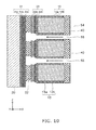
- FIG. 13 is a cross-sectional view showing a semiconductor memory device according to the embodiment.
- FIG. 13 shows a cross section corresponding to FIG. 3 .
- the semiconductor memory device 2 according to the embodiment differs from the semiconductor memory device 1 according to the first embodiment described above (referring to FIG. 1 to FIG. 3 ) in that the charge storage film 32 and the blocking insulating film 33 are not divided every electrode film 13 , and the silicon oxide layer 60 (referring to FIG. 11 ) is not provided.
- the configurations of the charge storage film 32 and the blocking insulating film 33 are circular tubes surrounding the silicon pillar 20 .
- the inner surface of an air gap 71 includes the silicon oxide film 12 , the barrier metal layer 13 b , and the aluminum oxide layer 33 b . Also, an end 71 c of the air gap 71 on the silicon pillar 20 side is positioned on the side surface of the blocking insulating film 33 on the electrode film 13 side; and a distance d 6 between the silicon pillar 20 and the air gap 71 is substantially equal to a distance d 7 between the silicon pillar 20 and the electrode film 13 . In other words, d 6 ⁇ d 7 .
- the distance d 3 between the source electrode plate 17 and the air gap 71 is shorter than the distance d 4 between the source electrode plate 17 and the electrode film 13 and longer than the distance d 5 between the capping film 40 and the source electrode plate 17 .
- d 5 ⁇ d 3 ⁇ d 4 is shorter than the distance d 5 between the capping film 40 and the source electrode plate 17 .
- the semiconductor memory device according to the embodiment can be manufactured as follows.
- the manufacturing is easy; and the productivity is high.
- the air gap 71 is disposed over the entire X-direction length of the region between the electrode films 13 adjacent to each other in the Z-direction in the XZ cross section including the silicon pillar 20 , the breakdown voltage between the electrode films 13 is high; and the parasitic capacitance is small.
- FIG. 14 is a cross-sectional view showing a semiconductor memory device according to the embodiment.
- FIG. 14 shows a cross section corresponding to FIG. 3 .
- the semiconductor memory device 3 according to the embodiment differs from the semiconductor memory device 2 according to the second embodiment described above (referring to FIG. 13 ) in that the capping film 40 is not provided.
- an end 17 d of the air gap 71 on the source electrode plate 17 side is further on the silicon pillar 20 side than is the surface 13 d of the electrode film 13 on the source electrode plate 17 side.
- the distance d 3 between the source electrode plate 17 and the air gap 71 is longer than the distance d 4 between the source electrode plate 17 and the electrode film 13 ; and d 3 >d 4 .
- the configuration of the embodiment is similar to that of the second embodiment described above.
- FIG. 15 is a cross-sectional view showing the method for manufacturing the semiconductor memory device according to the embodiment.
- the electrode films 13 are formed inside the space 55 by depositing titanium nitride and tungsten and by performing etch-back.
- the etch-back amount is less than those of the first and second embodiments described above; and the receded amount of the surfaces of the electrode films 13 exposed inside the slit 54 is less than those of the first and second embodiments described above.
- the silicon oxide films 51 are removed via the slit 54 by etching using conditions such that the etching rate of silicon oxide is higher than the etching rate of silicon nitride as shown in FIG. 15 .
- the space 58 is made between the electrode films 13 adjacent to each other in the Z-direction.
- silicon oxide is deposited thickly using conditions providing low coverage as shown in FIG. 14 .
- the silicon oxide film 61 is formed on the side surface of the slit 54 ; and the end of the space 58 on the slit 54 side is sealed.
- the space 58 becomes the air gap 71 .
- the capping film 40 does not exist, the end 17 d of the air gap 71 on the source electrode plate 17 side is positioned between the electrode films 13 adjacent to each other in the Z-direction.
- the manufacturing is easy; and the productivity is higher. Also, because the air gap 71 is made in a portion of the region between the electrode films 13 adjacent to each other in the Z-direction, the effect of increasing the breakdown voltage between the electrode films 13 and the effect of reducing the parasitic capacitance can be obtained somewhat.
- FIG. 16 is a perspective view showing a semiconductor memory device according to the embodiment.
- a below-cell circuit 90 is provided below the memory cell array in addition to the configuration of the semiconductor memory device 1 according to the first embodiment described above (referring to FIG. 1 ).
- an inter-layer insulating film 81 and a source electrode film 82 are provided between the silicon substrate 10 and the stacked body 15 .
- the inter-layer insulating film 81 is formed of silicon oxide; and, for example, the source electrode film 82 is formed of polysilicon to which an impurity is added.
- the silicon pillar 20 is connected not to the silicon substrate 10 but to the source electrode film 82 .
- the source electrode film 82 is insulated from the silicon substrate 10 by the inter-layer insulating film 81 .
- the source electrode film 82 is provided to be connected commonly to multiple stacked bodies and is further connected to, for example, a source line (not shown) of a lower layer.
- the below-cell circuit 90 is formed inside the inter-layer insulating film 81 and the upper layer portion of the silicon substrate 10 .
- the below-cell circuit 90 is a portion of the drive circuit that performs the programming, reading, and erasing of data to and from the memory cell transistors MC and includes, for example, sense amplifiers.
- the upper layer portion of the silicon substrate 10 is partitioned into multiple active areas by a STI (Shallow Trench Isolation) 84 ; a p-type MOSFET (Metal-Oxide-Semiconductor Field-Effect Transistor) 85 is formed in one active area; and an n-type MOSFET 86 is formed in another active area.
- multiple levels of interconnects are provided inside the inter-layer insulating film 81 ; contacts 88 that connect the interconnects 87 to the silicon substrate 10 are provided; and vias 89 that connect the interconnects 87 to each other are provided.
- the depictions of the p-type MOSFET 85 , the n-type MOSFET 86 , the interconnects 87 , etc., in FIG. 16 are schematic and do not necessarily match the sizes and dispositions of the actual elements.
- the source electrode plate 17 described in reference to FIG. 1 is not provided inside the slit 54 of the semiconductor memory device 4 ; and the source line 21 that is connected to the upper end of the source electrode plate 17 also is not provided.
- an insulator such as the silicon oxide plate 18 described in reference to FIG. 2 is filled into the slit 54 .
- the potential necessary for driving is supplied from the below-cell circuit 90 to the source electrode film 82 .
- the space between the silicon substrate 10 and the stacked body 15 can be utilized effectively; therefore, the surface area of the circuit disposed at the periphery of the stacked body 15 can be reduced by this amount. Also, the source electrode plate 17 and the source line 21 can be omitted. As a result, even higher integration of the semiconductor memory device 4 is possible. Otherwise, the configuration, the manufacturing method, and the effects of the embodiment are similar to those of the first embodiment described above.
- a semiconductor memory device having high integration and a method for manufacturing the semiconductor memory device can be realized.
Landscapes
- Non-Volatile Memory (AREA)
- Semiconductor Memories (AREA)
Abstract
Description
Claims (15)
Priority Applications (1)
| Application Number | Priority Date | Filing Date | Title |
|---|---|---|---|
| US15/210,446 US9865616B2 (en) | 2016-02-09 | 2016-07-14 | Semiconductor memory device and method for manufacturing same |
Applications Claiming Priority (2)
| Application Number | Priority Date | Filing Date | Title |
|---|---|---|---|
| US201662292955P | 2016-02-09 | 2016-02-09 | |
| US15/210,446 US9865616B2 (en) | 2016-02-09 | 2016-07-14 | Semiconductor memory device and method for manufacturing same |
Publications (2)
| Publication Number | Publication Date |
|---|---|
| US20170229474A1 US20170229474A1 (en) | 2017-08-10 |
| US9865616B2 true US9865616B2 (en) | 2018-01-09 |
Family
ID=59496298
Family Applications (1)
| Application Number | Title | Priority Date | Filing Date |
|---|---|---|---|
| US15/210,446 Active US9865616B2 (en) | 2016-02-09 | 2016-07-14 | Semiconductor memory device and method for manufacturing same |
Country Status (1)
| Country | Link |
|---|---|
| US (1) | US9865616B2 (en) |
Cited By (4)
| Publication number | Priority date | Publication date | Assignee | Title |
|---|---|---|---|---|
| US11189632B2 (en) | 2019-02-22 | 2021-11-30 | Samsung Electronics Co., Ltd. | Integrated circuit devices and methods of manufacturing the same |
| US11502097B2 (en) | 2019-08-27 | 2022-11-15 | Samsung Electronics Co., Ltd. | Integrated circuit device and method of manufacturing the same |
| US11653493B2 (en) | 2019-09-20 | 2023-05-16 | Samsung Electronics Co., Ltd. | Semiconductor memory device and method of manufacturing the same |
| US12193235B2 (en) | 2021-04-01 | 2025-01-07 | Samsung Electronics Co., Ltd. | Nonvolatile memory device and apparatus including the same |
Families Citing this family (17)
| Publication number | Priority date | Publication date | Assignee | Title |
|---|---|---|---|---|
| US9136128B2 (en) | 2011-08-31 | 2015-09-15 | Micron Technology, Inc. | Methods and apparatuses including memory cells with air gaps and other low dielectric constant materials |
| CN107958909B (en) * | 2016-10-17 | 2020-09-22 | 中芯国际集成电路制造(北京)有限公司 | Flash memory device and method of manufacturing the same |
| US10164009B1 (en) * | 2017-08-11 | 2018-12-25 | Micron Technology, Inc. | Memory device including voids between control gates |
| US10680006B2 (en) * | 2017-08-11 | 2020-06-09 | Micron Technology, Inc. | Charge trap structure with barrier to blocking region |
| US10453855B2 (en) * | 2017-08-11 | 2019-10-22 | Micron Technology, Inc. | Void formation in charge trap structures |
| US10446572B2 (en) * | 2017-08-11 | 2019-10-15 | Micron Technology, Inc. | Void formation for charge trap structures |
| US10903221B2 (en) | 2017-12-27 | 2021-01-26 | Micron Technology, Inc. | Memory cells and memory arrays |
| US10497715B2 (en) * | 2017-12-27 | 2019-12-03 | Micron Technology, Inc. | Memory arrays |
| US10438962B2 (en) * | 2017-12-27 | 2019-10-08 | Micron Technology, Inc. | Memory arrays, and methods of forming memory arrays |
| KR102677083B1 (en) * | 2018-09-14 | 2024-06-21 | 삼성전자주식회사 | Integrated circuit device and method of manufacturing the same |
| EP3844806B1 (en) | 2018-11-22 | 2024-01-17 | Yangtze Memory Technologies Co., Ltd. | Three-dimensional memory devices and fabricating methods thereof |
| US11244954B2 (en) * | 2019-08-22 | 2022-02-08 | Micron Technology, Inc. | Integrated assemblies having vertically-spaced channel material segments, and methods of forming integrated assemblies |
| KR102817656B1 (en) * | 2020-02-20 | 2025-06-10 | 에스케이하이닉스 주식회사 | Semiconductor device and manufacturing method thereof |
| KR102817652B1 (en) * | 2020-02-20 | 2025-06-10 | 에스케이하이닉스 주식회사 | Semiconductor device and manufacturing method of semiconductor device |
| KR102817674B1 (en) * | 2020-02-20 | 2025-06-10 | 에스케이하이닉스 주식회사 | Semiconductor device and manufacturing method of semiconductor device |
| KR20220006384A (en) * | 2020-07-08 | 2022-01-17 | 에스케이하이닉스 주식회사 | Semiconductor device and manufacturing method of semiconductor device |
| US11956954B2 (en) | 2020-11-09 | 2024-04-09 | Micron Technology, Inc. | Electronic devices comprising reduced charge confinement regions in storage nodes of pillars and related methods |
Citations (15)
| Publication number | Priority date | Publication date | Assignee | Title |
|---|---|---|---|---|
| JP2008277437A (en) | 2007-04-26 | 2008-11-13 | Renesas Technology Corp | Semiconductor device and manufacturing method thereof |
| US20100163968A1 (en) * | 2008-12-31 | 2010-07-01 | Samsung Electronics Co., Ltd. | Semiconductor memory device having insulation patterns and cell gate patterns |
| US20120052674A1 (en) | 2010-08-30 | 2012-03-01 | Jaegoo Lee | Semiconductor devices and methods of fabricating the same |
| JP2012080133A (en) | 2012-01-23 | 2012-04-19 | Hitachi Ltd | Manufacturing method of semiconductor device |
| JP2013128083A (en) | 2011-11-15 | 2013-06-27 | Toshiba Corp | Semiconductor device and method for manufacturing the same |
| US8569825B2 (en) | 2010-03-24 | 2013-10-29 | Kabushiki Kaisha Toshiba | Nonvolatile semiconductor storage device |
| JP2013543266A (en) | 2010-10-18 | 2013-11-28 | アイメック | Vertical semiconductor memory device and manufacturing method thereof |
| US20140061926A1 (en) | 2012-09-05 | 2014-03-06 | Kyu-hee Han | Semiconductor devices including supporting patterns in gap regions between conductive patterns and methods of fabricating the same |
| US20140220750A1 (en) | 2013-02-04 | 2014-08-07 | Woonghee Sohn | Semiconductor Memory Device and Method of Fabricating the Same |
| JP2014165457A (en) | 2013-02-27 | 2014-09-08 | Toshiba Corp | Manufacturing method of nonvolatile semiconductor memory device |
| US20140286098A1 (en) | 2013-03-25 | 2014-09-25 | Kabushiki Kaisha Toshiba | Nonvolatile semiconductor memory device |
| US20140308789A1 (en) | 2010-06-15 | 2014-10-16 | Kabushiki Kaisha Toshiba | Semiconductor memory device and method of manufacturing the same |
| US8896051B2 (en) * | 2011-12-20 | 2014-11-25 | Kabushiki Kaisha Toshiba | Semiconductor device and method for manufacturing the same |
| US9087736B1 (en) * | 2014-08-01 | 2015-07-21 | Macronix International Co., Ltd. | Three-dimensional memory device |
| US9570464B1 (en) | 2015-12-15 | 2017-02-14 | Kabushiki Kaisha Toshiba | Method for manufacturing semiconductor device |
-
2016
- 2016-07-14 US US15/210,446 patent/US9865616B2/en active Active
Patent Citations (19)
| Publication number | Priority date | Publication date | Assignee | Title |
|---|---|---|---|---|
| JP2008277437A (en) | 2007-04-26 | 2008-11-13 | Renesas Technology Corp | Semiconductor device and manufacturing method thereof |
| US20100163968A1 (en) * | 2008-12-31 | 2010-07-01 | Samsung Electronics Co., Ltd. | Semiconductor memory device having insulation patterns and cell gate patterns |
| US8569825B2 (en) | 2010-03-24 | 2013-10-29 | Kabushiki Kaisha Toshiba | Nonvolatile semiconductor storage device |
| US20140308789A1 (en) | 2010-06-15 | 2014-10-16 | Kabushiki Kaisha Toshiba | Semiconductor memory device and method of manufacturing the same |
| US20120052674A1 (en) | 2010-08-30 | 2012-03-01 | Jaegoo Lee | Semiconductor devices and methods of fabricating the same |
| JP2013543266A (en) | 2010-10-18 | 2013-11-28 | アイメック | Vertical semiconductor memory device and manufacturing method thereof |
| US20130341701A1 (en) | 2010-10-18 | 2013-12-26 | Imec | Vertical Semiconductor Memory Device and Manufacturing Method Thereof |
| US8809935B2 (en) | 2011-11-15 | 2014-08-19 | Kabushiki Kaisha Toshiba | Semiconductor device and method for manufacturing the same |
| JP2013128083A (en) | 2011-11-15 | 2013-06-27 | Toshiba Corp | Semiconductor device and method for manufacturing the same |
| US8896051B2 (en) * | 2011-12-20 | 2014-11-25 | Kabushiki Kaisha Toshiba | Semiconductor device and method for manufacturing the same |
| JP2012080133A (en) | 2012-01-23 | 2012-04-19 | Hitachi Ltd | Manufacturing method of semiconductor device |
| US20140061926A1 (en) | 2012-09-05 | 2014-03-06 | Kyu-hee Han | Semiconductor devices including supporting patterns in gap regions between conductive patterns and methods of fabricating the same |
| JP2014053612A (en) | 2012-09-05 | 2014-03-20 | Samsung Electronics Co Ltd | Semiconductor device and manufacturing method of the same |
| US20140220750A1 (en) | 2013-02-04 | 2014-08-07 | Woonghee Sohn | Semiconductor Memory Device and Method of Fabricating the Same |
| JP2014165457A (en) | 2013-02-27 | 2014-09-08 | Toshiba Corp | Manufacturing method of nonvolatile semiconductor memory device |
| US8895387B2 (en) | 2013-02-27 | 2014-11-25 | Kabushiki Kaisha Toshiba | Method of manufacturing nonvolatile semiconductor memory device |
| US20140286098A1 (en) | 2013-03-25 | 2014-09-25 | Kabushiki Kaisha Toshiba | Nonvolatile semiconductor memory device |
| US9087736B1 (en) * | 2014-08-01 | 2015-07-21 | Macronix International Co., Ltd. | Three-dimensional memory device |
| US9570464B1 (en) | 2015-12-15 | 2017-02-14 | Kabushiki Kaisha Toshiba | Method for manufacturing semiconductor device |
Cited By (5)
| Publication number | Priority date | Publication date | Assignee | Title |
|---|---|---|---|---|
| US11189632B2 (en) | 2019-02-22 | 2021-11-30 | Samsung Electronics Co., Ltd. | Integrated circuit devices and methods of manufacturing the same |
| US11728220B2 (en) | 2019-02-22 | 2023-08-15 | Samsung Electronics Co., Ltd. | Integrated circuit devices and methods of manufacturing the same |
| US11502097B2 (en) | 2019-08-27 | 2022-11-15 | Samsung Electronics Co., Ltd. | Integrated circuit device and method of manufacturing the same |
| US11653493B2 (en) | 2019-09-20 | 2023-05-16 | Samsung Electronics Co., Ltd. | Semiconductor memory device and method of manufacturing the same |
| US12193235B2 (en) | 2021-04-01 | 2025-01-07 | Samsung Electronics Co., Ltd. | Nonvolatile memory device and apparatus including the same |
Also Published As
| Publication number | Publication date |
|---|---|
| US20170229474A1 (en) | 2017-08-10 |
Similar Documents
| Publication | Publication Date | Title |
|---|---|---|
| US9865616B2 (en) | Semiconductor memory device and method for manufacturing same | |
| US11956959B2 (en) | Semiconductor memory device and method for manufacturing same | |
| US11374015B2 (en) | Semiconductor memory device | |
| US9184177B2 (en) | Semiconductor device and method for manufacturing the same | |
| CN107799529B (en) | Semiconductor memory device and method of manufacturing the same | |
| US11257840B2 (en) | Semiconductor device and method of fabricating the same | |
| TWI645474B (en) | Semiconductor device and its manufacturing method | |
| US10103155B2 (en) | Semiconductor memory device | |
| US10249641B2 (en) | Semiconductor memory device and method for manufacturing same | |
| US8643081B2 (en) | Semiconductor memory device | |
| US20220285380A1 (en) | Semiconductor memory device | |
| TW201816938A (en) | Semiconductor device | |
| JP2015095650A (en) | Nonvolatile semiconductor memory device | |
| US9997536B2 (en) | Semiconductor memory device | |
| US9911752B2 (en) | Semiconductor memory device and method for manufacturing same | |
| US9953996B2 (en) | Semiconductor memory device | |
| US20160268296A1 (en) | Semiconductor memory device and method for manufacturing same | |
| TWI746072B (en) | Semiconductor memory device and manufacturing method of semiconductor memory device | |
| TWI755031B (en) | semiconductor memory device | |
| JP7502122B2 (en) | Semiconductor device and its manufacturing method | |
| US20190221576A1 (en) | Semiconductor memory device and method for driving same | |
| US10109578B2 (en) | Semiconductor memory device |
Legal Events
| Date | Code | Title | Description |
|---|---|---|---|
| AS | Assignment |
Owner name: KABUSHIKI KAISHA TOSHIBA, JAPAN Free format text: ASSIGNMENT OF ASSIGNORS INTEREST;ASSIGNORS:SHIMIZU, TAKASHI;MEGURO, HISATAKA;TAKAHASHI, SHINYA;AND OTHERS;REEL/FRAME:039160/0648 Effective date: 20160511 |
|
| AS | Assignment |
Owner name: TOSHIBA MEMORY CORPORATION, JAPAN Free format text: ASSIGNMENT OF ASSIGNORS INTEREST;ASSIGNOR:KABUSHIKI KAISHA TOSHIBA;REEL/FRAME:043355/0058 Effective date: 20170713 |
|
| STCF | Information on status: patent grant |
Free format text: PATENTED CASE |
|
| AS | Assignment |
Owner name: K.K. PANGEA, JAPAN Free format text: MERGER;ASSIGNOR:TOSHIBA MEMORY CORPORATION;REEL/FRAME:055659/0471 Effective date: 20180801 Owner name: TOSHIBA MEMORY CORPORATION, JAPAN Free format text: CHANGE OF NAME AND ADDRESS;ASSIGNOR:K.K. PANGEA;REEL/FRAME:055669/0401 Effective date: 20180801 Owner name: KIOXIA CORPORATION, JAPAN Free format text: CHANGE OF NAME AND ADDRESS;ASSIGNOR:TOSHIBA MEMORY CORPORATION;REEL/FRAME:055669/0001 Effective date: 20191001 |
|
| MAFP | Maintenance fee payment |
Free format text: PAYMENT OF MAINTENANCE FEE, 4TH YEAR, LARGE ENTITY (ORIGINAL EVENT CODE: M1551); ENTITY STATUS OF PATENT OWNER: LARGE ENTITY Year of fee payment: 4 |
|
| MAFP | Maintenance fee payment |
Free format text: PAYMENT OF MAINTENANCE FEE, 8TH YEAR, LARGE ENTITY (ORIGINAL EVENT CODE: M1552); ENTITY STATUS OF PATENT OWNER: LARGE ENTITY Year of fee payment: 8 |