US10089930B2 - Brightness compensation in a display - Google Patents
Brightness compensation in a display Download PDFInfo
- Publication number
- US10089930B2 US10089930B2 US14/440,513 US201314440513A US10089930B2 US 10089930 B2 US10089930 B2 US 10089930B2 US 201314440513 A US201314440513 A US 201314440513A US 10089930 B2 US10089930 B2 US 10089930B2
- Authority
- US
- United States
- Prior art keywords
- pixel
- pixels
- brightness
- voltage drop
- display device
- Prior art date
- Legal status (The legal status is an assumption and is not a legal conclusion. Google has not performed a legal analysis and makes no representation as to the accuracy of the status listed.)
- Active
Links
Images


Classifications
-
- G—PHYSICS
- G09—EDUCATION; CRYPTOGRAPHY; DISPLAY; ADVERTISING; SEALS
- G09G—ARRANGEMENTS OR CIRCUITS FOR CONTROL OF INDICATING DEVICES USING STATIC MEANS TO PRESENT VARIABLE INFORMATION
- G09G3/00—Control arrangements or circuits, of interest only in connection with visual indicators other than cathode-ray tubes
- G09G3/20—Control arrangements or circuits, of interest only in connection with visual indicators other than cathode-ray tubes for presentation of an assembly of a number of characters, e.g. a page, by composing the assembly by combination of individual elements arranged in a matrix no fixed position being assigned to or needed to be assigned to the individual characters or partial characters
- G09G3/22—Control arrangements or circuits, of interest only in connection with visual indicators other than cathode-ray tubes for presentation of an assembly of a number of characters, e.g. a page, by composing the assembly by combination of individual elements arranged in a matrix no fixed position being assigned to or needed to be assigned to the individual characters or partial characters using controlled light sources
- G09G3/30—Control arrangements or circuits, of interest only in connection with visual indicators other than cathode-ray tubes for presentation of an assembly of a number of characters, e.g. a page, by composing the assembly by combination of individual elements arranged in a matrix no fixed position being assigned to or needed to be assigned to the individual characters or partial characters using controlled light sources using electroluminescent panels
- G09G3/32—Control arrangements or circuits, of interest only in connection with visual indicators other than cathode-ray tubes for presentation of an assembly of a number of characters, e.g. a page, by composing the assembly by combination of individual elements arranged in a matrix no fixed position being assigned to or needed to be assigned to the individual characters or partial characters using controlled light sources using electroluminescent panels semiconductive, e.g. using light-emitting diodes [LED]
- G09G3/3208—Control arrangements or circuits, of interest only in connection with visual indicators other than cathode-ray tubes for presentation of an assembly of a number of characters, e.g. a page, by composing the assembly by combination of individual elements arranged in a matrix no fixed position being assigned to or needed to be assigned to the individual characters or partial characters using controlled light sources using electroluminescent panels semiconductive, e.g. using light-emitting diodes [LED] organic, e.g. using organic light-emitting diodes [OLED]
- G09G3/3225—Control arrangements or circuits, of interest only in connection with visual indicators other than cathode-ray tubes for presentation of an assembly of a number of characters, e.g. a page, by composing the assembly by combination of individual elements arranged in a matrix no fixed position being assigned to or needed to be assigned to the individual characters or partial characters using controlled light sources using electroluminescent panels semiconductive, e.g. using light-emitting diodes [LED] organic, e.g. using organic light-emitting diodes [OLED] using an active matrix
- G09G3/3258—Control arrangements or circuits, of interest only in connection with visual indicators other than cathode-ray tubes for presentation of an assembly of a number of characters, e.g. a page, by composing the assembly by combination of individual elements arranged in a matrix no fixed position being assigned to or needed to be assigned to the individual characters or partial characters using controlled light sources using electroluminescent panels semiconductive, e.g. using light-emitting diodes [LED] organic, e.g. using organic light-emitting diodes [OLED] using an active matrix with pixel circuitry controlling the voltage across the light-emitting element
-
- G—PHYSICS
- G09—EDUCATION; CRYPTOGRAPHY; DISPLAY; ADVERTISING; SEALS
- G09G—ARRANGEMENTS OR CIRCUITS FOR CONTROL OF INDICATING DEVICES USING STATIC MEANS TO PRESENT VARIABLE INFORMATION
- G09G3/00—Control arrangements or circuits, of interest only in connection with visual indicators other than cathode-ray tubes
- G09G3/20—Control arrangements or circuits, of interest only in connection with visual indicators other than cathode-ray tubes for presentation of an assembly of a number of characters, e.g. a page, by composing the assembly by combination of individual elements arranged in a matrix no fixed position being assigned to or needed to be assigned to the individual characters or partial characters
- G09G3/22—Control arrangements or circuits, of interest only in connection with visual indicators other than cathode-ray tubes for presentation of an assembly of a number of characters, e.g. a page, by composing the assembly by combination of individual elements arranged in a matrix no fixed position being assigned to or needed to be assigned to the individual characters or partial characters using controlled light sources
- G09G3/30—Control arrangements or circuits, of interest only in connection with visual indicators other than cathode-ray tubes for presentation of an assembly of a number of characters, e.g. a page, by composing the assembly by combination of individual elements arranged in a matrix no fixed position being assigned to or needed to be assigned to the individual characters or partial characters using controlled light sources using electroluminescent panels
- G09G3/32—Control arrangements or circuits, of interest only in connection with visual indicators other than cathode-ray tubes for presentation of an assembly of a number of characters, e.g. a page, by composing the assembly by combination of individual elements arranged in a matrix no fixed position being assigned to or needed to be assigned to the individual characters or partial characters using controlled light sources using electroluminescent panels semiconductive, e.g. using light-emitting diodes [LED]
- G09G3/3208—Control arrangements or circuits, of interest only in connection with visual indicators other than cathode-ray tubes for presentation of an assembly of a number of characters, e.g. a page, by composing the assembly by combination of individual elements arranged in a matrix no fixed position being assigned to or needed to be assigned to the individual characters or partial characters using controlled light sources using electroluminescent panels semiconductive, e.g. using light-emitting diodes [LED] organic, e.g. using organic light-emitting diodes [OLED]
- G09G3/3225—Control arrangements or circuits, of interest only in connection with visual indicators other than cathode-ray tubes for presentation of an assembly of a number of characters, e.g. a page, by composing the assembly by combination of individual elements arranged in a matrix no fixed position being assigned to or needed to be assigned to the individual characters or partial characters using controlled light sources using electroluminescent panels semiconductive, e.g. using light-emitting diodes [LED] organic, e.g. using organic light-emitting diodes [OLED] using an active matrix
- G09G3/3233—Control arrangements or circuits, of interest only in connection with visual indicators other than cathode-ray tubes for presentation of an assembly of a number of characters, e.g. a page, by composing the assembly by combination of individual elements arranged in a matrix no fixed position being assigned to or needed to be assigned to the individual characters or partial characters using controlled light sources using electroluminescent panels semiconductive, e.g. using light-emitting diodes [LED] organic, e.g. using organic light-emitting diodes [OLED] using an active matrix with pixel circuitry controlling the current through the light-emitting element
- G09G3/3241—Control arrangements or circuits, of interest only in connection with visual indicators other than cathode-ray tubes for presentation of an assembly of a number of characters, e.g. a page, by composing the assembly by combination of individual elements arranged in a matrix no fixed position being assigned to or needed to be assigned to the individual characters or partial characters using controlled light sources using electroluminescent panels semiconductive, e.g. using light-emitting diodes [LED] organic, e.g. using organic light-emitting diodes [OLED] using an active matrix with pixel circuitry controlling the current through the light-emitting element the current through the light-emitting element being set using a data current provided by the data driver, e.g. by using a two-transistor current mirror
- G09G3/325—Control arrangements or circuits, of interest only in connection with visual indicators other than cathode-ray tubes for presentation of an assembly of a number of characters, e.g. a page, by composing the assembly by combination of individual elements arranged in a matrix no fixed position being assigned to or needed to be assigned to the individual characters or partial characters using controlled light sources using electroluminescent panels semiconductive, e.g. using light-emitting diodes [LED] organic, e.g. using organic light-emitting diodes [OLED] using an active matrix with pixel circuitry controlling the current through the light-emitting element the current through the light-emitting element being set using a data current provided by the data driver, e.g. by using a two-transistor current mirror the data current flowing through the driving transistor during a setting phase, e.g. by using a switch for connecting the driving transistor to the data driver
-
- G—PHYSICS
- G09—EDUCATION; CRYPTOGRAPHY; DISPLAY; ADVERTISING; SEALS
- G09G—ARRANGEMENTS OR CIRCUITS FOR CONTROL OF INDICATING DEVICES USING STATIC MEANS TO PRESENT VARIABLE INFORMATION
- G09G3/00—Control arrangements or circuits, of interest only in connection with visual indicators other than cathode-ray tubes
- G09G3/20—Control arrangements or circuits, of interest only in connection with visual indicators other than cathode-ray tubes for presentation of an assembly of a number of characters, e.g. a page, by composing the assembly by combination of individual elements arranged in a matrix no fixed position being assigned to or needed to be assigned to the individual characters or partial characters
- G09G3/22—Control arrangements or circuits, of interest only in connection with visual indicators other than cathode-ray tubes for presentation of an assembly of a number of characters, e.g. a page, by composing the assembly by combination of individual elements arranged in a matrix no fixed position being assigned to or needed to be assigned to the individual characters or partial characters using controlled light sources
- G09G3/30—Control arrangements or circuits, of interest only in connection with visual indicators other than cathode-ray tubes for presentation of an assembly of a number of characters, e.g. a page, by composing the assembly by combination of individual elements arranged in a matrix no fixed position being assigned to or needed to be assigned to the individual characters or partial characters using controlled light sources using electroluminescent panels
- G09G3/32—Control arrangements or circuits, of interest only in connection with visual indicators other than cathode-ray tubes for presentation of an assembly of a number of characters, e.g. a page, by composing the assembly by combination of individual elements arranged in a matrix no fixed position being assigned to or needed to be assigned to the individual characters or partial characters using controlled light sources using electroluminescent panels semiconductive, e.g. using light-emitting diodes [LED]
- G09G3/3208—Control arrangements or circuits, of interest only in connection with visual indicators other than cathode-ray tubes for presentation of an assembly of a number of characters, e.g. a page, by composing the assembly by combination of individual elements arranged in a matrix no fixed position being assigned to or needed to be assigned to the individual characters or partial characters using controlled light sources using electroluminescent panels semiconductive, e.g. using light-emitting diodes [LED] organic, e.g. using organic light-emitting diodes [OLED]
- G09G3/3275—Details of drivers for data electrodes
- G09G3/3283—Details of drivers for data electrodes in which the data driver supplies a variable data current for setting the current through, or the voltage across, the light-emitting elements
-
- G—PHYSICS
- G09—EDUCATION; CRYPTOGRAPHY; DISPLAY; ADVERTISING; SEALS
- G09G—ARRANGEMENTS OR CIRCUITS FOR CONTROL OF INDICATING DEVICES USING STATIC MEANS TO PRESENT VARIABLE INFORMATION
- G09G3/00—Control arrangements or circuits, of interest only in connection with visual indicators other than cathode-ray tubes
- G09G3/20—Control arrangements or circuits, of interest only in connection with visual indicators other than cathode-ray tubes for presentation of an assembly of a number of characters, e.g. a page, by composing the assembly by combination of individual elements arranged in a matrix no fixed position being assigned to or needed to be assigned to the individual characters or partial characters
- G09G3/22—Control arrangements or circuits, of interest only in connection with visual indicators other than cathode-ray tubes for presentation of an assembly of a number of characters, e.g. a page, by composing the assembly by combination of individual elements arranged in a matrix no fixed position being assigned to or needed to be assigned to the individual characters or partial characters using controlled light sources
- G09G3/30—Control arrangements or circuits, of interest only in connection with visual indicators other than cathode-ray tubes for presentation of an assembly of a number of characters, e.g. a page, by composing the assembly by combination of individual elements arranged in a matrix no fixed position being assigned to or needed to be assigned to the individual characters or partial characters using controlled light sources using electroluminescent panels
- G09G3/32—Control arrangements or circuits, of interest only in connection with visual indicators other than cathode-ray tubes for presentation of an assembly of a number of characters, e.g. a page, by composing the assembly by combination of individual elements arranged in a matrix no fixed position being assigned to or needed to be assigned to the individual characters or partial characters using controlled light sources using electroluminescent panels semiconductive, e.g. using light-emitting diodes [LED]
- G09G3/3208—Control arrangements or circuits, of interest only in connection with visual indicators other than cathode-ray tubes for presentation of an assembly of a number of characters, e.g. a page, by composing the assembly by combination of individual elements arranged in a matrix no fixed position being assigned to or needed to be assigned to the individual characters or partial characters using controlled light sources using electroluminescent panels semiconductive, e.g. using light-emitting diodes [LED] organic, e.g. using organic light-emitting diodes [OLED]
- G09G3/3275—Details of drivers for data electrodes
- G09G3/3291—Details of drivers for data electrodes in which the data driver supplies a variable data voltage for setting the current through, or the voltage across, the light-emitting elements
-
- G—PHYSICS
- G09—EDUCATION; CRYPTOGRAPHY; DISPLAY; ADVERTISING; SEALS
- G09G—ARRANGEMENTS OR CIRCUITS FOR CONTROL OF INDICATING DEVICES USING STATIC MEANS TO PRESENT VARIABLE INFORMATION
- G09G2300/00—Aspects of the constitution of display devices
- G09G2300/08—Active matrix structure, i.e. with use of active elements, inclusive of non-linear two terminal elements, in the pixels together with light emitting or modulating elements
- G09G2300/0809—Several active elements per pixel in active matrix panels
- G09G2300/0819—Several active elements per pixel in active matrix panels used for counteracting undesired variations, e.g. feedback or autozeroing
-
- G—PHYSICS
- G09—EDUCATION; CRYPTOGRAPHY; DISPLAY; ADVERTISING; SEALS
- G09G—ARRANGEMENTS OR CIRCUITS FOR CONTROL OF INDICATING DEVICES USING STATIC MEANS TO PRESENT VARIABLE INFORMATION
- G09G2320/00—Control of display operating conditions
- G09G2320/02—Improving the quality of display appearance
- G09G2320/0209—Crosstalk reduction, i.e. to reduce direct or indirect influences of signals directed to a certain pixel of the displayed image on other pixels of said image, inclusive of influences affecting pixels in different frames or fields or sub-images which constitute a same image, e.g. left and right images of a stereoscopic display
-
- G—PHYSICS
- G09—EDUCATION; CRYPTOGRAPHY; DISPLAY; ADVERTISING; SEALS
- G09G—ARRANGEMENTS OR CIRCUITS FOR CONTROL OF INDICATING DEVICES USING STATIC MEANS TO PRESENT VARIABLE INFORMATION
- G09G2320/00—Control of display operating conditions
- G09G2320/02—Improving the quality of display appearance
- G09G2320/0223—Compensation for problems related to R-C delay and attenuation in electrodes of matrix panels, e.g. in gate electrodes or on-substrate video signal electrodes
-
- G—PHYSICS
- G09—EDUCATION; CRYPTOGRAPHY; DISPLAY; ADVERTISING; SEALS
- G09G—ARRANGEMENTS OR CIRCUITS FOR CONTROL OF INDICATING DEVICES USING STATIC MEANS TO PRESENT VARIABLE INFORMATION
- G09G2320/00—Control of display operating conditions
- G09G2320/02—Improving the quality of display appearance
- G09G2320/0233—Improving the luminance or brightness uniformity across the screen
Definitions
- a display device such as an Active Matrix Organic Light Emitting Diode (AMOLED) display, may include several pixels. The pixels may be periodically refreshed in order to display a stationary or dynamic picture.
- AMOLED Active Matrix Organic Light Emitting Diode
- FIG. 1 is a circuit diagram of a portion of a display device according to various embodiments of the present disclosure.
- FIG. 2 is a circuit diagram of an example of a pixel in the display device of FIG. 1 according to various embodiments of the present disclosure.
- FIG. 3 is a flowchart illustrating an example of functionality implemented by a controller in the display device of FIG. 1 according to various embodiments of the present disclosure.
- FIG. 4 is a schematic block diagram of an example of the display device of FIG. 1 according to various embodiments of the present disclosure.
- AMOLED Active matrix organic light emitting diode
- OLED organic light emitting diode
- Pixels are arranged in a matrix, where the refreshing of the screen is done in a row-by-row fashion. Each pixel in a row is refreshed simultaneously within a given time slot, after which the pixel is kept at the prescribed brightness level until the next refresh cycle, thus the name active matrix, in comparison with passive matrix where each pixel only maintain its brightness when it is addressed.
- a pixel in an AMOLED display is set to the brightness level appropriate to the specific overall scene to be conveyed and that brightness level must be maintained (“memorized”) until the next refresh resets the pixel for the next scene.
- each pixel contains a circuit, called the pixel circuit, to drive its OLED.
- Pixel circuits are connected by bus lines that provide the signal and power to each circuit.
- the pixel circuits and bus lines form the backplane of the AMOLED.
- the display device 100 may comprise, for example, an active matrix organic light emitting diode (AMOLED) panel or any type of display device wherein the instantaneous pixel light output is dependent upon the current through the light emitting subcomponent within the pixel, the bus line supplying that current is shared with other pixels, and multiple pixels along that line are simultaneously lit.
- AMOLED active matrix organic light emitting diode
- the display device 100 includes a matrix of pixels 103 arranged in columns C 1 -C x and rows R 1 -R y .
- the display device 100 also includes a supply voltage line 109 (also termed V DD ) that is coupled to pixels 103 in each of the columns C 1 -C x . Additionally, each row R 1 -R y of pixels 103 includes a scan line 113 , and each column of pixels 103 includes a data line 116 .
- V DD supply voltage line
- All of the pixels 103 in a particular row R 1 -R y of the display device 100 are refreshed simultaneously within a given timeslot, after which these pixels 103 are kept at the prescribed brightness level until the particular row R 1 -R y is refreshed in the next refresh cycle.
- a brightness signal is applied to each data line 116 , and one of the scan lines 113 is asserted.
- the brightness signals applied to the data lines 116 are provided to the corresponding pixels 103 in the corresponding row R 1 -R y .
- new brightness signals are applied to the data lines 116 , and the scan line 113 for the next row R 1 -R y is asserted.
- the pixels 103 for the new row R 1 -R y having the asserted scan line 113 are provided with the brightness signals being applied to the data lines 116 .
- This process is then repeated for all of the remaining rows R 1 -R y of the display device 100 to thereby generate a picture.
- the process may be further repeated for all of the pixels 103 with varying signals on the data lines 116 to generate a dynamic picture.
- the pixel 103 may include one of the data lines 116 , the supply voltage line 109 , and one of the scan lines 113 .
- the pixel 103 may include a switching transistor 203 , a driving transistor 206 , a capacitor 209 , a light emitting device 213 , and potentially other components not discussed in detail for brevity. It is understood that other circuit configurations and components may be used for the pixel 103 in alternative embodiments.
- the light emitting device 213 is configured to emit light in response to a current flowing through the light emitting device 213 .
- the light emitting device 213 may be embodied in the form of, for example, an organic light emitting diode (OLED), a inorganic light emitting diode (LED), a quantum dot based light emitting diode or any other type of light emitting device.
- OLED organic light emitting diode
- LED inorganic light emitting diode
- quantum dot based light emitting diode any other type of light emitting device.
- the driving transistor 206 is configured to provide and control the amount of current that flows through the light emitting device 213 .
- a first terminal 206 a of the driving transistor 206 is coupled to the supply voltage line 109
- a second terminal 206 b for the driving transistor 206 is coupled to the light emitting device 213 .
- the amount of current that flows from the first terminal 206 a to the second terminal 206 b of the driving transistor 206 is dependent on the voltage level being applied to a third terminal 206 c of the driving transistor 206 .
- the current flowing through the driving transistor 206 may be modeled using the following equation:
- I is the current through the driving transistor 206
- V DATA is the voltage of the brightness signal from the data line 116
- V DD is the voltage on the supply voltage line 109
- the areal capacitance of the gate dielectric is C
- the mobility of the transistor is ⁇
- the transistor channel width to channel length ratio is
- the switching transistor 203 is configured to selectively provide the third terminal 206 c of the driving transistor 206 with a signal from the data line 116 .
- a first terminal 203 a of the switching transistor 203 is coupled to the data line 116
- a second terminal 203 b of the switching transistor 203 is coupled to the third terminal 206 c of the driving transistor 206
- a third terminal 203 c of the switching transistor 203 is coupled to the scan line 113 .
- the switching transistor 203 may turn “on” or “off” in response to the signal being provided on the scan line 113 .
- the signal from the data line 116 passes through the switching transistor 203 to the third terminal 206 c of the driving transistor 206 when the scan line 113 signal is asserted, causing the switching transistor 203 to be “on.”
- the switching transistor 203 is “off,” and the signal on the data line 116 is prevented from being received at the third terminal 206 c of the driving transistor 206 .
- the capacitor 209 stores the voltage value (i.e., the brightness signal) that is provided to the third terminal 206 c of the driving transistor 206 when the switching transistor 203 is “on” and substantially maintains this voltage value when the switching transistor 203 is “off.” Because the capacitor 209 is coupled to the third terminal 206 c of the driving transistor 206 , the capacitor 209 helps to maintain a particular value of current flowing through the light emitting device 213 between refresh cycles for the display device 100 .
- a brightness signal is provided to the data line 116 , and the scan line 113 is asserted to turn the switching transistor 203 “on” and thereby cause the brightness signal on the data line 116 to be provided to the third terminal 206 c of the driving transistor 206 .
- a current flows from the first terminal 206 a to the second terminal 206 b of the driving transistor 206 and through the light emitting device 213 .
- This current relationship may be modeled, for example, by EQN 1.
- the brightness of the light emitted from the light emitting device 213 is dependent upon the amount of current flowing from the driving transistor 206 , the brightness of the light is also dependent upon the supply voltage value at the first terminal 206 a and the brightness signal at the third terminal 206 c of the driving transistor 206 .
- EQN 2 may be substituted for V DD in EQN 1 to account for IR drop.
- ⁇ V i can be rewritten as ⁇ V i,i where the first index indicates the pixel for which the voltage has been affected, and the second index indicates the pixel at which current has changed that caused this voltage change.
- the supply voltage line 109 may also facilitate unintentional cross-talk due to the refreshing of the pixels 103 .
- the change in the supply voltage for a first pixel 103 at location i due to a change in current for a second pixel 103 at location m, wherein the first pixel 103 and the second pixel 103 are in the same column C 1 -C y may be expressed as:
- ⁇ V i,m is the change in the supply voltage for the first pixel 103 at location i with respect to the change in the current ( ⁇ I m ) for the second pixel 103 at location m.
- the change in the current at a pixel with respect to a change in the supply voltage may be approximated by taking the derivative of EQN 1 with respect to V DD .
- ⁇ I i,m ⁇ k[ ⁇ V i,m ⁇ ( V DATA(i) ⁇ V DD(i,m ⁇ 1) ⁇ V TH )+ ⁇ V i,m 2 ], (EQN 4)
- ⁇ I i,m is the change in current for the first pixel 103 at location i due to the change in current ( ⁇ I m ) for the second pixel at location m
- ⁇ V i,m corresponds to EQN 3
- V DD(i,m ⁇ 1) represents the voltage on the supply voltage line 109 seen by the pixel at location i right before the pixel at location m changes its current, with the IR drop being considered.
- EQN 4 provides an estimate of the change in current for a pixel 103 when the effects of IR drop and cross-talk are accounted for.
- EQN 4 may be used to identify the effects of IR drop and cross-talk on a pixel 103 .
- a compensated brightness signal may be applied to the data line 116 that results in the average actual current value provided by the driving transistor 206 being substantially the same as a target current.
- the following example assumes that the display device 100 has previously refreshed the pixels 103 using non-compensated brightness signals and that the display device 100 is prepared to initiate a pixel 103 refresh.
- the display device 100 may identify a new target current value (I target(m) new ) that is expected to result in the pixel 103 in the column emitting the desired light brightness. To this end, the display device 100 may, for example, query a look-up table having values stored therein, or the display device may calculate this value using, for example, an equation that models pixel 103 brightness as a function of the driving current.
- a new target current value I target(m) new
- V DD(i,i ⁇ 1) may be calculated using EQN 2 and substituting the actual power supply line value of every pixel in the column at that time or, in a continuously refreshing column, V DD(i,i ⁇ 1) may be recorded and updated in a lookup table for every pixel.
- V DD(i,i ⁇ 1) may be recorded and updated in a lookup table for every pixel.
- the display device 100 may then identify the changes in the expected current value for the pixel 103 after each of the other pixels 103 in the column C 1 -C y is refreshed. Thus, if there are y pixels 103 in the column C 1 -C y , there may be y changes in the expected current value that are identified. In order to calculate these changes, EQN 4 or EQN 5 may be used, for example. After the pixel at location i is refreshed, the circuit can continue to update the pixel at location i+1 after a time interval of
- the updating continues through pixel n and pixel 1 until reaching the pixel at location i ⁇ 1, which is the last pixel in this refresh cycle.
- the display device 100 may identify the average of the current changes. This relationship may be determined as the average of the currents, for example, using the following equation:
- the display device 100 identifies a value for the new brightness signal to be applied on the data line 116 .
- a value for the brightness signal may be identified that takes into account the effects of the IR drop and cross-talk for a pixel 103 .
- the identified value for V DATA can be applied to the data line 116 as a compensating brightness signal, and the pixel 103 can be refreshed.
- the average current for the pixel 103 may be substantially the same as the target current that would result in the desired brightness of the pixel 103 .
- a viewer may visually perceive the pixel 103 as being the desired brightness.
- the other pixels 103 may be refreshed using a similar procedure as described above. Repeating the same steps for all pixels in the column will compensate the entire column of pixels for the IR drop.
- the IR-drop and crosstalk compensation scheme thus operates by anticipation as follows: by looking ahead at upcoming data line signals it knows the desired brightness of each pixel. From that zeroth order data it estimates the IR drop occurring at each pixel due to the specific current drawn by the other pixels along the supply line. From that information a correction factor is calculated or provided, which once applied to the data signals compensates for the change in brightness due to that calculated IR drop. The scheme thus results in an average pixel brightness that approximates the desired brightness.
- the current supplied to each pixel can be calculated to be 8 ⁇ A.
- the resistance of the supply voltage line 109 between two adjacent pixels is 500 ⁇ . While this may be unrealistically high compared with that of a real supply voltage line 109 , the high resistance emphasizes the IR drop between pixels. From EQN 1, the V DATA can be determined to be 6.5672V from:
- V DATA 6.5672 V applied to all four pixels. Due to the IR drop of the supply voltage line 109 , the actual V DD voltage seen by each pixel will be different, resulting in different pixel currents. The IR drop on the supply voltage line 109 will reduce the current through pixel 1 almost 3%, while the current to pixel 4 is reduced by more than 7%. TABLE 1 provides examples of the different values due to the IR drop.
- the expressions for ⁇ I average(i) according to EQN 7 can be determined, and the appropriate V DATA for each pixel found by solving EQN 8.
- the average values are calculated based on the last refreshing cycle for each pixel. For all pixels, the deviation was found to be less than 0.05% as shown in TABLE 2.
- FIG. 3 shown is a flowchart illustrating an example of functionality implemented by a brightness controller 300 ( FIG. 4 ) in the display device 100 ( FIG. 1 ) according to various embodiments of the present disclosure.
- the brightness controller 300 may comprise, for example, a processing device and/or logic executable in a processing device. It is understood that the flowchart of FIG. 3 provides merely an example of the many different types of functional arrangements that may be employed to implement the operation of the portion of the brightness controller 300 as described herein. As an alternative, the flowchart of FIG. 3 may be viewed as depicting an example of steps of a method implemented in the display device 100 according to one or more embodiments.
- the brightness controller 300 identifies a first brightness signal for the pixel 103 .
- the first brightness signal may be, for example, the value for a non-compensated brightness signal previously used to refresh the pixel 103 .
- a first target current value is identified for the pixel 103 based at least in part on the first brightness signal identified in box 303 .
- the brightness controller 300 then moves to box 309 and identifies a second target current value for the pixel 103 based at least in part on a desired brightness for the pixel 103 .
- the brightness controller 300 may query a lookup table or calculate the second target current value, for example.
- the brightness controller 300 identifies the difference between the first target current value and the second target current value. This relationship is represented by EQN 6 above.
- the brightness controller 300 then identifies a change in the expected supply voltage for the pixel 103 in response to the pixel 103 being refreshed with the second target current value.
- the brightness controller 300 then moves to box 319 and identifies changes in the expected current value for the pixel 103 due to each one of the other pixels 103 in the column C 1 -C y being refreshed.
- the brightness controller 300 may, for example, apply EQN 4 or EQN 5 above.
- the average expected current value for the pixel 103 after refreshing each of the other pixels 103 in the column C 1 -C y is identified.
- the brightness controller 300 may, for example, apply EQN 7 above in order to identify the average expected current values and express them as functions of the second brightness signals, such as V DATA for each pixel 103 in the column.
- the brightness controller 300 identifies a second brightness signal for the pixel 103 based at least in part on the identified average change for the expected current value, which was identified in box 323 .
- EQN 8 may be employed in order to calculate the brightness signal such as V DATA .
- the brightness controller 300 applies the second brightness signal on the data line 116 for the pixel 103 . Thereafter the process ends.
- CMOS complementary metal-oxide-semiconductor
- TFT backplanes or other transistor enabled backplanes such as a carbon nanotube enabled vertical organic light emitting transistor (CN-VOLET) backplane.
- CN-VOLET carbon nanotube enabled vertical organic light emitting transistor
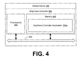
- the display device 100 includes at least one processor circuit, for example, having a processor 403 and a memory 406 , both of which are coupled to a local interface 409 .
- the local interface 409 may comprise, for example, a data bus with an accompanying address/control bus or other bus structure as can be appreciated.
- Stored in the memory 406 are both data and several components that are executable by the processor 403 .
- stored in the memory 406 and executable by the processor 403 may be a brightness controller application 300 a , and potentially other applications.
- any component discussed herein is implemented in the form of software, any one of a number of programming languages may be employed such as, for example, C, C++, C#, Objective C, Java, Javascript, Perl, PHP, Visual Basic, Python, Ruby, Delphi, Flash, or other programming languages.
- executable means a program file that is in a form that can ultimately be run by the processor 403 .
- Examples of executable programs may be, for example, a compiled program that can be translated into machine code in a format that can be loaded into a random access portion of the memory 406 and run by the processor 403 , source code that may be expressed in proper format such as object code that is capable of being loaded into a random access portion of the memory 406 and executed by the processor 403 , or source code that may be interpreted by another executable program to generate instructions in a random access portion of the memory 406 to be executed by the processor 403 , etc.
- An executable program may be stored in any portion or component of the memory 406 including, for example, random access memory (RAM), read-only memory (ROM), hard drive, solid-state drive, USB flash drive, memory card, optical disc such as compact disc (CD) or digital versatile disc (DVD), floppy disk, magnetic tape, or other memory components.
- RAM random access memory
- ROM read-only memory
- hard drive solid-state drive
- USB flash drive USB flash drive
- memory card such as compact disc (CD) or digital versatile disc (DVD), floppy disk, magnetic tape, or other memory components.
- CD compact disc
- DVD digital versatile disc
- the memory 406 is defined herein as including both volatile and nonvolatile memory and data storage components. Volatile components are those that do not retain data values upon loss of power. Nonvolatile components are those that retain data upon a loss of power.
- the memory 406 may comprise, for example, random access memory (RAM), read-only memory (ROM), hard disk drives, solid-state drives, USB flash drives, memory cards accessed via a memory card reader, floppy disks accessed via an associated floppy disk drive, optical discs accessed via an optical disc drive, magnetic tapes accessed via an appropriate tape drive, and/or other memory components, or a combination of any two or more of these memory components.
- the RAM may comprise, for example, static random access memory (SRAM), dynamic random access memory (DRAM), or magnetic random access memory (MRAM) and other such devices.
- the ROM may comprise, for example, a programmable read-only memory (PROM), an erasable programmable read-only memory (EPROM), an electrically erasable programmable read-only memory (EEPROM), or other like memory device.
- the processor 403 may represent multiple processors 403
- the memory 406 may represent multiple memories 406 that operate in parallel processing circuits, respectively.
- the local interface 409 may be an appropriate network that facilitates communication between any two of the multiple processors 403 , between any processor 403 and any of the memories 406 , or between any two of the memories 406 , etc.
- the local interface 409 may comprise additional systems designed to coordinate this communication, including, for example, performing load balancing.
- the processor 403 may be of electrical or of some other available construction.
- the brightness controller 300 may be embodied in software or code executed by general purpose hardware as discussed above, as an alternative the same may also be embodied in dedicated hardware or a combination of software/general purpose hardware and dedicated hardware. If embodied in dedicated hardware, each can be implemented as a circuit or state machine that employs any one of or a combination of a number of technologies. These technologies may include, but are not limited to, discrete logic circuits having logic gates for implementing various logic functions upon an application of one or more data signals, application specific integrated circuits having appropriate logic gates, or other components, etc. Such technologies are generally well known by those skilled in the art and, consequently, are not described in detail herein.
- each block may represent a module, segment, or portion of code that comprises program instructions to implement the specified logical function(s).
- the program instructions may be embodied in the form of source code that comprises human-readable statements written in a programming language or machine code that comprises numerical instructions recognizable by a suitable execution system such as a processor 403 in a computer system or other system.
- the machine code may be converted from the source code, etc.
- each block may represent a circuit or a number of interconnected circuits to implement the specified logical function(s).
- FIG. 3 shows a specific order of execution, it is understood that the order of execution may differ from that which is depicted. For example, the order of execution of two or more blocks may be scrambled relative to the order shown. Also, two or more blocks shown in succession in FIG. 3 may be executed concurrently or with partial concurrence. Further, in some embodiments, one or more of the blocks shown in FIG. 3 may be skipped or omitted. In addition, any number of counters, state variables, warning semaphores, or messages might be added to the logical flow described herein, for purposes of enhanced utility, accounting, performance measurement, or providing troubleshooting aids, etc. It is understood that all such variations are within the scope of the present disclosure.
- any logic or application described herein, including the brightness controller application 300 a , that comprises software or code can be embodied in any non-transitory computer-readable medium for use by or in connection with an instruction execution system such as, for example, a processor 403 in a computer system or other system.
- the logic may comprise, for example, statements including instructions and declarations that can be fetched from the computer-readable medium and executed by the instruction execution system.
- a “computer-readable medium” can be any medium that can contain, store, or maintain the logic or application described herein for use by or in connection with the instruction execution system.
- the computer-readable medium can comprise any one of many physical media such as, for example, magnetic, optical, or semiconductor media.
- a suitable computer-readable medium would include, but are not limited to, magnetic tapes, magnetic floppy diskettes, magnetic hard drives, memory cards, solid-state drives, USB flash drives, or optical discs.
- the computer-readable medium may be a random access memory (RAM) including, for example, static random access memory (SRAM) and dynamic random access memory (DRAM), or magnetic random access memory (MRAM).
- the computer-readable medium may be a read-only memory (ROM), a programmable read-only memory (PROM), an erasable programmable read-only memory (EPROM), an electrically erasable programmable read-only memory (EEPROM), or other type of memory device.
- Embodiments of the present disclosure include, but are not limited to, a method comprising identifying, in a display device, an IR voltage drop effect on a pixel in the display device based at least in part on a plurality of currents drawn by a plurality of other pixels being supplied by a same supply voltage line and generating, in the display device, a brightness signal for the pixel based at least in part on the IR voltage drop effect, wherein the brightness signal compensates for the IR voltage drop effect.
- Another embodiment includes a method comprising calculating, in a display device, values of the IR voltage drop for each pixel due to the specific currents to be drawn by all the pixels fed by the same supply voltage line, necessary to display the next specific frame of the scene at the requisite pixel brightness appropriate to the scene and providing a data line signal to each pixel that compensates for the IR voltage drop based upon that calculation and thereby ensuring the requisite perceived pixel brightness appropriate to the specific frame of the scene.
- the brightness signal may be based at least in part on an average of a plurality of current values for the pixel in response to a plurality of other pixels being refreshed.
- the brightness signal may be a voltage and/or a current.
- the pixel(s) may comprise an organic light emitting diode (OLED).
- the display device may comprise an active matrix organic light emitting diode (AMOLED) panel.
- the pixel may comprise a vertical light emitting transistor.
- the pixel may comprise an active matrix light emitting transistor panel.
- the instantaneous brightness of a specific pixel may change as other pixels sharing the supply voltage line are refreshed, while the average perceived brightness of the specific pixel, which was set by the data line signal, based upon the calculation, is appropriate for the specific frame of the scene.
- aspects of the present disclosure can be used for other pixel architecture implementations.
- aspects of the present disclosure may be used for an active matrix display that uses an integrated drive transistor and light emitter, such as that described in U.S. Pat. No. 8,232,561, entitled “NANOTUBE ENABLED, GATE-VOLTAGE CONTROLLED LIGHT EMITTING DIODES,” filed on Sep.
Priority Applications (1)
| Application Number | Priority Date | Filing Date | Title |
|---|---|---|---|
| US14/440,513 US10089930B2 (en) | 2012-11-05 | 2013-11-05 | Brightness compensation in a display |
Applications Claiming Priority (3)
| Application Number | Priority Date | Filing Date | Title |
|---|---|---|---|
| US201261722496P | 2012-11-05 | 2012-11-05 | |
| US14/440,513 US10089930B2 (en) | 2012-11-05 | 2013-11-05 | Brightness compensation in a display |
| PCT/US2013/068402 WO2014071343A1 (en) | 2012-11-05 | 2013-11-05 | Brightness compensation in a display |
Publications (2)
| Publication Number | Publication Date |
|---|---|
| US20150269887A1 US20150269887A1 (en) | 2015-09-24 |
| US10089930B2 true US10089930B2 (en) | 2018-10-02 |
Family
ID=50628151
Family Applications (1)
| Application Number | Title | Priority Date | Filing Date |
|---|---|---|---|
| US14/440,513 Active US10089930B2 (en) | 2012-11-05 | 2013-11-05 | Brightness compensation in a display |
Country Status (6)
| Country | Link |
|---|---|
| US (1) | US10089930B2 (zh) |
| EP (1) | EP2915161B1 (zh) |
| JP (2) | JP6426102B2 (zh) |
| KR (1) | KR102084288B1 (zh) |
| CN (1) | CN104769661B (zh) |
| WO (1) | WO2014071343A1 (zh) |
Families Citing this family (18)
| Publication number | Priority date | Publication date | Assignee | Title |
|---|---|---|---|---|
| KR102057286B1 (ko) * | 2013-02-21 | 2019-12-19 | 삼성디스플레이 주식회사 | 유기전계발광 표시장치 |
| CN105097872B (zh) * | 2014-05-23 | 2019-11-15 | 伊格尼斯创新公司 | 提取有机发光器件的关联曲线的系统和方法 |
| CN104867455B (zh) * | 2015-06-16 | 2017-05-03 | 深圳市华星光电技术有限公司 | 补偿amoled电压降的系统及方法 |
| KR102512487B1 (ko) * | 2015-12-30 | 2023-03-23 | 엘지디스플레이 주식회사 | 유기발광 표시장치와 그 구동방법 |
| CN105405405B (zh) * | 2016-01-04 | 2018-06-08 | 京东方科技集团股份有限公司 | 电压降补偿方法及装置、显示装置 |
| US10068554B2 (en) * | 2016-08-02 | 2018-09-04 | Qualcomm Incorporated | Systems and methods for conserving power in refreshing a display panel |
| CN107180613B (zh) * | 2017-05-26 | 2019-03-12 | 京东方科技集团股份有限公司 | 有机发光二极管显示面板及其驱动方法 |
| CN107909974B (zh) * | 2017-11-21 | 2020-09-08 | 海信视像科技股份有限公司 | 像素补偿方法、装置及电视 |
| WO2020059072A1 (ja) | 2018-09-20 | 2020-03-26 | シャープ株式会社 | 表示装置およびその駆動方法 |
| US11308881B2 (en) | 2018-09-20 | 2022-04-19 | Sharp Kabushiki Kaisha | Display device and method for driving same |
| WO2020218421A1 (en) * | 2019-04-26 | 2020-10-29 | Jsr Corporation | Method of compensating brightness of display and display |
| JP2020183968A (ja) * | 2019-04-26 | 2020-11-12 | Jsr株式会社 | ディスプレイの輝度補償方法及びディスプレイ |
| CN110364111B (zh) * | 2019-08-30 | 2023-03-07 | 京东方科技集团股份有限公司 | 显示面板像素补偿方法及补偿装置 |
| CN110599961B (zh) * | 2019-09-20 | 2021-05-07 | 京东方科技集团股份有限公司 | 显示面板的灰阶补偿方法、装置及系统 |
| KR20210065586A (ko) * | 2019-11-27 | 2021-06-04 | 삼성전자주식회사 | 표시 패널 및 표시 장치 |
| CN111627396B (zh) * | 2020-06-29 | 2021-08-20 | 武汉天马微电子有限公司 | 一种数据线电压确定方法、确定装置及驱动方法 |
| JP7367635B2 (ja) * | 2020-08-21 | 2023-10-24 | Jsr株式会社 | ディスプレイ |
| CN116075877A (zh) | 2020-08-21 | 2023-05-05 | Jsr株式会社 | 显示器 |
Citations (168)
| Publication number | Priority date | Publication date | Assignee | Title |
|---|---|---|---|---|
| US3700979A (en) | 1971-04-07 | 1972-10-24 | Rca Corp | Schottky barrier diode and method of making the same |
| US3841904A (en) | 1972-12-11 | 1974-10-15 | Rca Corp | Method of making a metal silicide-silicon schottky barrier |
| JPS5532235B1 (zh) | 1977-05-18 | 1980-08-23 | ||
| US4471367A (en) | 1981-12-04 | 1984-09-11 | At&T Bell Laboratories | MESFET Using a shallow junction gate structure on GaInAs |
| US5210045A (en) | 1987-10-06 | 1993-05-11 | General Electric Company | Dual dielectric field effect transistors for protected gate structures for improved yield and performance in thin film transistor matrix addressed liquid crystal displays |
| US5429968A (en) | 1991-07-12 | 1995-07-04 | Nec Corporation | Method of forming a mask programmable read only memory device with multi-level memory cell array |
| US5793055A (en) | 1995-11-30 | 1998-08-11 | Forschungszentrum Julich Gmbh | Hybrid electronic devices, particularly Josephson transistors |
| WO2001008192A1 (en) | 1999-07-26 | 2001-02-01 | Advanced Vision Technologies, Inc. | Insulated-gate electron field emission devices and their fabrication processes |
| CN1324550A (zh) | 1998-10-21 | 2001-11-28 | 诺基亚网络有限公司 | 数字电信系统 |
| US20020070382A1 (en) | 2000-12-11 | 2002-06-13 | Shunpei Yamazaki | Semiconductor device, and manufacturing method thereof |
| US6480412B1 (en) | 1999-10-27 | 2002-11-12 | Sony Corporation | Magnetization control method, information storage method, magnetic functional device, and information storage device |
| US20020173083A1 (en) | 2001-01-03 | 2002-11-21 | International Business Machines Corporation | Methodology for electrically induced selective breakdown of nanotubes |
| US6492669B2 (en) | 2000-06-29 | 2002-12-10 | Nec Corporation | Semiconductor device with schottky electrode having high schottky barrier |
| US20020195644A1 (en) | 2001-06-08 | 2002-12-26 | Ananth Dodabalapur | Organic polarizable gate transistor apparatus and method |
| JP2003108034A (ja) | 2001-07-17 | 2003-04-11 | Semiconductor Energy Lab Co Ltd | 発光装置 |
| JP2003258265A (ja) | 2001-12-28 | 2003-09-12 | National Institute Of Advanced Industrial & Technology | 有機薄膜トランジスタ |
| JP2003330412A (ja) | 2002-05-10 | 2003-11-19 | Canon Inc | アクティブマトリックス型ディスプレイ及びスイッチ回路 |
| JP2003332350A (ja) | 2002-05-17 | 2003-11-21 | Hitachi Ltd | 薄膜半導体装置 |
| US6744111B1 (en) | 2003-05-15 | 2004-06-01 | Koucheng Wu | Schottky-barrier tunneling transistor |
| CN1501341A (zh) | 2002-10-07 | 2004-06-02 | ����Sdi��ʽ���� | 平板显示器 |
| US20040113152A1 (en) | 2002-12-14 | 2004-06-17 | Kim Seong Hyun | Vertical structure thin film transistor |
| US20040183758A1 (en) * | 2003-03-21 | 2004-09-23 | Industrial Technology Research Institute | Pixel circuit for active matrix OLED and driving method |
| US6800499B2 (en) | 1999-05-28 | 2004-10-05 | National Science Council | Process for preparing a hydrogen sensor |
| US20040197546A1 (en) | 2002-07-19 | 2004-10-07 | University Of Florida | Transparent electrodes from single wall carbon nanotubes |
| US20050001299A1 (en) | 2003-07-04 | 2005-01-06 | Amkor Technology, Inc. | Substrate for semiconductor package wire bonding method using thereof |
| CN1581512A (zh) | 2003-08-01 | 2005-02-16 | 杨金玉 | 用离子束改性技术控制半金属场效应管沟道材料的载流子密度 |
| JP2005064452A (ja) | 2003-08-19 | 2005-03-10 | Hitachi Ltd | ナノチューブトランジスタデバイスおよびその製造方法 |
| WO2005024907A2 (en) | 2003-08-29 | 2005-03-17 | The Regents Of The University Of California | Vertical organic field effect transistor |
| JP2005128310A (ja) | 2003-10-24 | 2005-05-19 | Seiko Epson Corp | 表示装置、及び電子機器 |
| US20050140600A1 (en) * | 2003-11-27 | 2005-06-30 | Yang-Wan Kim | Light emitting display, display panel, and driving method thereof |
| US20050146264A1 (en) * | 2004-01-05 | 2005-07-07 | Won-Kyu Kwak | Organic electro luminescence display |
| JP2005228804A (ja) | 2004-02-10 | 2005-08-25 | Sharp Corp | メモリ素子の製造方法およびそれに用いられるメモリ素子の製造装置 |
| US20050206300A1 (en) | 2004-03-18 | 2005-09-22 | C.R.F. Societa Consortile Per Azioni | Light-emitting device using a three-dimension percolated layer, and manufacturing process thereof |
| WO2005091373A1 (ja) | 2004-03-22 | 2005-09-29 | Rohm Co., Ltd | 有機半導体素子およびそれを用いた有機el表示装置 |
| JP2005268550A (ja) | 2004-03-18 | 2005-09-29 | Japan Science & Technology Agency | 有機半導体及びそれを用いた半導体装置並びにそれらの製造方法 |
| KR20050098333A (ko) | 2004-04-06 | 2005-10-12 | 삼성에스디아이 주식회사 | 능동형 유기 el 픽셀 |
| US20050245087A1 (en) | 2004-04-28 | 2005-11-03 | Semiconductor Energy Laboratory Co., Ltd. | Wiring over substrate, semiconductor device, and methods for manufacturing thereof |
| CN1698217A (zh) | 2001-12-19 | 2005-11-16 | 艾夫西亚有限公司 | 使用有机电介质的有机场效应晶体管 |
| JP2005535139A (ja) | 2002-08-07 | 2005-11-17 | コーニンクレッカ フィリップス エレクトロニクス エヌ ヴィ | 電界効果トランジスタ |
| US20060023511A1 (en) | 2004-08-02 | 2006-02-02 | Zhigang Wang | Flash memory unit and method of programming a flash memory device |
| US20060065887A1 (en) | 2004-03-26 | 2006-03-30 | Thomas Tiano | Carbon nanotube-based electronic devices made by electrolytic deposition and applications thereof |
| US20060081882A1 (en) | 2004-10-15 | 2006-04-20 | General Electric Company | High performance field effect transistors comprising carbon nanotubes fabricated using solution based processing |
| US20060102067A1 (en) | 2004-11-11 | 2006-05-18 | Samsung Electronics Co., Ltd. | Organic light emitting display with single crystalline silicon TFT and method of fabricating the same |
| US7060241B2 (en) | 2001-03-26 | 2006-06-13 | Eikos, Inc. | Coatings comprising carbon nanotubes and methods for forming same |
| US7068452B2 (en) | 2004-08-25 | 2006-06-27 | Hitachi, Ltd. | Method for recording magnetic information and magnetic recording system |
| JP2006171745A (ja) | 2004-12-14 | 2006-06-29 | Samsung Sdi Co Ltd | 有機電界発光素子及びその製造方法 |
| CN1797723A (zh) | 2004-12-23 | 2006-07-05 | 北京大学 | 基于碳纳米管的单电子晶体管制备方法 |
| US20060145144A1 (en) | 2005-01-05 | 2006-07-06 | Samsung Electronics Co., Ltd. | Vertical organic thin film transistor and organic light emitting transistor |
| KR100608001B1 (ko) | 2004-08-17 | 2006-08-02 | 삼성전자주식회사 | 오디오 앰프의 전류 제한 장치 및 그 방법 |
| CN1816913A (zh) | 2003-07-01 | 2006-08-09 | 微米技术股份有限公司 | 非易失性半导体存储器 |
| JP2006210910A (ja) | 2005-01-26 | 2006-08-10 | Samsung Electronics Co Ltd | カーボンナノチューブチャネルを用いたマルチビット不揮発性メモリ素子及びその動作方法 |
| US7098151B2 (en) | 2002-08-01 | 2006-08-29 | Semiconductor Energy Laboratory Co., Ltd. | Method of manufacturing carbon nanotube semiconductor device |
| US7102157B2 (en) | 2004-01-26 | 2006-09-05 | Alexander Kastalsky | Nanotube-based vacuum devices |
| US7115916B2 (en) | 2002-09-26 | 2006-10-03 | International Business Machines Corporation | System and method for molecular optical emission |
| US7119402B2 (en) | 2003-09-05 | 2006-10-10 | Kabushiki Kaisha Toshiba | Field effect transistor and manufacturing method thereof |
| JP2006301629A (ja) | 2005-04-16 | 2006-11-02 | Samsung Electronics Co Ltd | 単結晶シリコン薄膜トランジスタの有機発光ディスプレイ及びその製造方法 |
| US20060243971A1 (en) | 2001-12-17 | 2006-11-02 | Hiroyuki Iechi | Organic transistor |
| EP1718126A1 (en) | 2004-01-21 | 2006-11-02 | Kyoto University | Organic semiconductor device, display using same, and imager |
| US20060244391A1 (en) | 2005-05-02 | 2006-11-02 | Semiconductor Energy Laboratory Co., Ltd. | Display device, and driving method and electronic apparatus of the display device |
| US20060263255A1 (en) | 2002-09-04 | 2006-11-23 | Tzong-Ru Han | Nanoelectronic sensor system and hydrogen-sensitive functionalization |
| CN1875496A (zh) | 2003-08-29 | 2006-12-06 | 加利福尼亚大学董事会 | 垂直有机场效应晶体管 |
| US20060292362A1 (en) | 2005-06-28 | 2006-12-28 | Che-Hsiung Hsu | Bilayer anode |
| US20070012922A1 (en) | 2004-01-15 | 2007-01-18 | Matsushita Electric Industrial Co., Ltd. | Field effect transistor and display using same |
| CN1912977A (zh) | 2005-08-12 | 2007-02-14 | 精工爱普生株式会社 | 信号传送电路、电光学装置以及电子机器 |
| WO2007048041A2 (en) | 2005-10-21 | 2007-04-26 | The Regents Of The University Of California | Ambipolar vertical organic field-effect transistors |
| JP2007109454A (ja) | 2005-10-12 | 2007-04-26 | Toyota Motor Corp | リチウム二次電池およびその製造方法 |
| US20070138462A1 (en) | 2005-12-21 | 2007-06-21 | Palo Alto Research Center Incorporated | Electronic device with unique encoding |
| US20070146247A1 (en) * | 2005-11-28 | 2007-06-28 | Huang Chien H | Organic light emitting display |
| US20070147159A1 (en) | 2005-12-28 | 2007-06-28 | Lee Young-Dae | Standby leakage current reduction circuit and semiconductor memory device comprising the standby leakage current reduction circuit |
| US20070146252A1 (en) | 2005-12-22 | 2007-06-28 | Eastman Kodak Company | Electroluminescent display brightness level adjustment |
| WO2007080575A1 (en) | 2006-01-09 | 2007-07-19 | Technion Research And Development Foundation Ltd. | Transistor structures and methods of fabrication thereof |
| US7247913B2 (en) | 2004-07-13 | 2007-07-24 | Kabushiki Kaisha Toshiba | Semiconductor device having a Schottky source/drain transistor |
| JP2007200788A (ja) | 2006-01-30 | 2007-08-09 | Dainippon Printing Co Ltd | 有機発光トランジスタ素子及びその製造方法並びに発光表示装置 |
| US7259984B2 (en) | 2002-11-26 | 2007-08-21 | Cornell Research Foundation, Inc. | Multibit metal nanocrystal memories and fabrication |
| US20070215954A1 (en) | 2006-03-16 | 2007-09-20 | Micron Technology, Inc. | Stacked non-volatile memory with silicon carbide-based amorphous silicon thin film transistors |
| US7323730B2 (en) | 2004-07-21 | 2008-01-29 | Commissariat A L'energie Atomique | Optically-configurable nanotube or nanowire semiconductor device |
| US7359888B2 (en) | 2003-01-31 | 2008-04-15 | Hewlett-Packard Development Company, L.P. | Molecular-junction-nanowire-crossbar-based neural network |
| US20080100542A1 (en) * | 2006-11-01 | 2008-05-01 | Miller Michael E | Electro-luminescent display with voltage adjustment |
| WO2008050726A1 (fr) | 2006-10-25 | 2008-05-02 | Hiroshima University | Nouveau composé aromatique à cycle fusionne, son procédé de production et son utilisation |
| US7378328B2 (en) | 2002-02-09 | 2008-05-27 | Samsung Electronics Co., Ltd. | Method of fabricating memory device utilizing carbon nanotubes |
| US20080143389A1 (en) | 2006-12-19 | 2008-06-19 | Ali Keshavarzi | Logic circuits using carbon nanotube transistors |
| US20080150846A1 (en) * | 2006-12-21 | 2008-06-26 | Boyong Chung | Organic light emitting display and driving method thereof |
| US20080169822A1 (en) * | 2007-01-15 | 2008-07-17 | Wonkyu Kwak | Substrate testing device and method thereof |
| US7405129B2 (en) | 2004-11-18 | 2008-07-29 | International Business Machines Corporation | Device comprising doped nano-component and method of forming the device |
| CN101276638A (zh) | 2006-12-27 | 2008-10-01 | 海力士半导体有限公司 | 具有铁电器件的半导体存储器器件及其更新方法 |
| US20080252203A1 (en) * | 2007-04-13 | 2008-10-16 | Samsung Sdi Co., Ltd. | Organic light emitting diode display |
| US7439562B2 (en) | 2003-04-22 | 2008-10-21 | Commissariat A L'energie Atomique | Process for modifying at least one electrical property of a nanotube or a nanowire and a transistor incorporating it |
| US7473922B2 (en) | 2005-12-09 | 2009-01-06 | Fujitsu Limited | Infrared detector |
| CN101375426A (zh) | 2005-11-28 | 2009-02-25 | 大日本印刷株式会社 | 有机发光晶体管元件及其制造方法 |
| WO2009036071A2 (en) | 2007-09-10 | 2009-03-19 | University Of Florida Research Foundation, Inc. | Nanotube enabled, gate-voltage controlled light emitting diodes |
| US20090072229A1 (en) * | 2007-09-14 | 2009-03-19 | Samsung Sdi Co., Ltd. | Thin film transistor, method of fabricating the thin film transistor, organic light emitting diode display device, method of fabricating the organic light emitting diode display device, and donor substrate for laser induced thermal imaging |
| US20090085182A1 (en) | 2007-07-27 | 2009-04-02 | Shunpei Yamazaki | Semiconductor device and method for manufacturing the same |
| US20090125858A1 (en) * | 2007-11-12 | 2009-05-14 | Texas Instruments Incorporated | IC Design Flow Incorporating Optimal Assumptions of Power Supply Voltage Drops at Cells when Performing Timing Analysis |
| US7538337B2 (en) | 2004-06-15 | 2009-05-26 | Nxp B.V. | Nanowire semiconductor device |
| US20090134387A1 (en) | 2007-11-26 | 2009-05-28 | Sanyo Electric Co., Ltd. | Cmos semiconductor device |
| US7545051B2 (en) | 2003-06-20 | 2009-06-09 | The Regents Of The University Of California | Nanowire array and nanowire solar cells and methods for forming the same |
| US7545241B2 (en) | 2004-03-11 | 2009-06-09 | Nec Corporation | Nanoparticle transmission line element and method of fabricating the same |
| US20090159971A1 (en) | 2007-12-19 | 2009-06-25 | Palo Alto Research Center Incorporated | Printed tft and tft array with self-aligned gate |
| US20090184903A1 (en) * | 2008-01-18 | 2009-07-23 | Samsung Mobile Display Co., Ltd. | Organic light emitting display and driving method thereof |
| US20090206341A1 (en) | 2008-01-31 | 2009-08-20 | Marks Tobin J | Solution-processed high mobility inorganic thin-film transistors |
| US20090230384A1 (en) | 2008-03-14 | 2009-09-17 | National Chiao Tung University | Vertical organic light emitting transistor assembly and horizontal organic light emitting transistor assembly |
| US20090256140A1 (en) * | 2008-04-10 | 2009-10-15 | National Chiao Tung University | Light-detecting device structure |
| US20090302310A1 (en) | 2006-06-29 | 2009-12-10 | Andrew Rinzler | Short Channel Vertical FETs |
| US20090302749A1 (en) * | 2008-06-10 | 2009-12-10 | Kyu-Sung Lee | Organic light emitting display apparatus |
| US20090315025A1 (en) | 2008-06-19 | 2009-12-24 | Fujifilm Corporation | Liquid crystalline organic semiconductor material and organic electron device |
| US7645933B2 (en) | 2005-03-02 | 2010-01-12 | Wisconsin Alumni Research Foundation | Carbon nanotube Schottky barrier photovoltaic cell |
| US20100042345A1 (en) * | 2008-08-14 | 2010-02-18 | Kang Jung-Soo | Apparatus and method for estimating resistance characteristics of battery based on open circuit voltage estimated by battery voltage variation pattern |
| US20100053137A1 (en) | 2008-09-03 | 2010-03-04 | Samsung Electronics Co., Ltd. | Display device and driving method thereof |
| JP2010062549A (ja) | 2008-08-08 | 2010-03-18 | Semiconductor Energy Lab Co Ltd | 半導体装置の作製方法 |
| US20100085009A1 (en) * | 2008-08-08 | 2010-04-08 | Kang Jung-Soo | Cell balancing apparatus and method |
| US20100123120A1 (en) | 2005-09-27 | 2010-05-20 | Northwestern University | A single-photon detector with a quantum dot and a nano-injector |
| US20100126885A1 (en) | 2008-11-21 | 2010-05-27 | Hiroyuki Iechi | Sensor device and method of measuring a solution |
| US20100127243A1 (en) | 2008-11-26 | 2010-05-27 | The Board Of Regents The University Of Texas System | Bi-layer pseudo-spin field-effect transistor |
| US20100148183A1 (en) | 2001-07-25 | 2010-06-17 | Ward Jonathan W | Method of Forming a Carbon Nanotube-Based Contact to Semiconductor |
| US20100155696A1 (en) | 2002-09-30 | 2010-06-24 | Nanosys, Inc. | Large-Area Nanoenabled Macroelectronic Substrates and Uses Therefor |
| US20100171419A1 (en) * | 2009-01-07 | 2010-07-08 | Kim Eun-Ah | Organic light emitting diode display and method of manufacturing the same |
| US20100177024A1 (en) * | 2009-01-12 | 2010-07-15 | Sang-Moo Choi | Organic light emitting display |
| US20100277513A1 (en) * | 2009-04-29 | 2010-11-04 | Seungchan Byun | Organic light emitting diode display and driving method |
| US20100309233A1 (en) | 2009-02-16 | 2010-12-09 | Neoviewkolon Co., Ltd. | Pixel circuit for organic light emitting diode (oled) panel, display device having the same, and method of driving oled panel using the same |
| US20110018787A1 (en) | 2009-07-22 | 2011-01-27 | Hitachi Displays, Ltd. | Display device |
| US20110050659A1 (en) * | 2009-08-26 | 2011-03-03 | Au Optronics Corp. | Pixel Circuit, Active Matrix Organic Light Emitting Diode Display and Driving Method for Pixel Circuit |
| US20110050736A1 (en) * | 2009-09-01 | 2011-03-03 | National Taiwan University Of Science And Technology | Pixel and illuminating device thereof |
| US20110063197A1 (en) * | 2009-09-14 | 2011-03-17 | Bo-Yong Chung | Pixel circuit and organic light emitting display apparatus including the same |
| JP2011095506A (ja) | 2009-10-29 | 2011-05-12 | Hitachi Displays Ltd | 表示装置 |
| US20110115772A1 (en) * | 2009-11-16 | 2011-05-19 | Chung Kyung-Hoon | Pixel Circuit and Organic Electroluminescent Display Apparatus Using the Same |
| US20110115764A1 (en) * | 2009-11-16 | 2011-05-19 | Chung Kyung-Hoon | Pixel Circuit and Organic Electroluminescent Display Apparatus Using the Same |
| US20110121271A1 (en) | 2009-11-25 | 2011-05-26 | Hee-Song Jeon | Organic light emitting diode display |
| US20110130981A1 (en) | 2009-11-30 | 2011-06-02 | Ignis Innovation Inc. | System and methods for aging compensation in amoled displays |
| US20110128268A1 (en) * | 2009-12-01 | 2011-06-02 | Hyung-Soo Kim | Organic light emitting display |
| US20110153303A1 (en) * | 2009-12-22 | 2011-06-23 | Mstar Semiconductor, Inc. | Static IR (voltage) drop Analyzing Apparatus and Associated Method |
| US20110164071A1 (en) * | 2010-01-04 | 2011-07-07 | Bo-Yong Chung | Pixel circuit, organic electro-luminescent display apparatus, and method of driving the same |
| US20110169798A1 (en) * | 2009-09-08 | 2011-07-14 | Au Optronics Corp. | Active Matrix Organic Light Emitting Diode (OLED) Display, Pixel Circuit and Data Current Writing Method Thereof |
| US20110191042A1 (en) | 2010-02-04 | 2011-08-04 | Ignis Innovation Inc. | System and methods for extracting correlation curves for an organic light emitting device |
| WO2011109693A2 (en) | 2010-03-04 | 2011-09-09 | University Of Florida Research Foundation Inc. | Semiconductor devices including an electrically percolating source layer and methods of fabricating the same |
| US8022432B2 (en) | 2005-08-19 | 2011-09-20 | Lg Display Co., Ltd. | Light-emitting device comprising conductive nanorods as transparent electrodes |
| US20110234644A1 (en) * | 2010-03-25 | 2011-09-29 | Kyong-Tae Park | Display device, image signal correction system, and image signal correction method |
| US20110248243A1 (en) | 2009-11-30 | 2011-10-13 | Omega Optics, Inc. | Carbon nanotube field effect transistor for printed flexible/rigid electronics |
| US20110248269A1 (en) * | 2010-04-08 | 2011-10-13 | Il-Soo Oh | Organic light emitting diode display and method for manufacturing the same |
| US8058167B2 (en) | 2003-10-22 | 2011-11-15 | Avolare 2, Llc | Dynamic Schottky barrier MOSFET device and method of manufacture |
| US20110291115A1 (en) * | 2010-06-01 | 2011-12-01 | Hyung-Soo Kim | Organic light emitting display |
| US20120013597A1 (en) * | 2010-07-19 | 2012-01-19 | Sam-Il Han | Pixel and organic light emitting display using the same |
| US20120012919A1 (en) | 2009-03-27 | 2012-01-19 | Cornell University | Nonvolatile flash memory structures including fullerene molecules and methods for manufacturing the same |
| US20120044269A1 (en) | 2010-08-20 | 2012-02-23 | Korea Advanced Institute Of Science And Technology | Organic light emitting diode driver |
| US20120050344A1 (en) * | 2010-08-24 | 2012-03-01 | Samsung Mobile Display Co., Ltd. | Organic Light Emitting Display Having Uniform Brightness |
| US20120062613A1 (en) * | 2010-09-14 | 2012-03-15 | Jong-Hwa Park | Organic light emitting display device and driving method thereof |
| US20120086694A1 (en) * | 2010-10-08 | 2012-04-12 | Au Optronics Corp. | Pixel circuit and display panel with ir-drop compensation function |
| US20120101022A1 (en) | 2009-04-02 | 2012-04-26 | The Johns Hopkins University | Self-assembling peptides bearing organic electronic functionality and applications employing the same |
| US20120143568A1 (en) | 2009-05-20 | 2012-06-07 | The Trustees Of The University Of Pennsylvania | Self-adaptive bio-signal and modulation device |
| WO2012078759A2 (en) | 2010-12-07 | 2012-06-14 | University Of Florida Research Foundation, Inc. | Active matrix dilute source enabled vertical organic light emitting transistor |
| US20120168778A1 (en) * | 2010-12-29 | 2012-07-05 | Do-Ik Kim | Organic light emitting diode display |
| US20120242712A1 (en) * | 2011-03-24 | 2012-09-27 | Hannstar Display Corporation | Pixel circuit of light emitting diode display and driving method thereof |
| US20120249514A1 (en) | 2011-04-01 | 2012-10-04 | Jung-Keun Ahn | Organic light emitting display device, data driving apparatus for organic light emitting display device, and driving method thereof |
| US20120287103A1 (en) * | 2011-05-13 | 2012-11-15 | Boe Technology Group Co., Ltd. | Pixel unit circuit, pixel array, display panel and display panel driving method |
| US20120293482A1 (en) * | 2011-05-18 | 2012-11-22 | Boe Technology Group Co., Ltd. | Pixel unit circuit and oled display apparatus |
| US20130020967A1 (en) * | 2011-07-21 | 2013-01-24 | Hae-Goo Jung | Organic light emitting diode display |
| US20130063040A1 (en) * | 2011-09-13 | 2013-03-14 | Wintek Corporation | Light-emitting component driving circuit and related pixel circuit and applications |
| US20130069852A1 (en) * | 2011-09-19 | 2013-03-21 | Wintek Corporation | Light-emitting component driving circuit and related pixel circuit and applications |
| US20130088417A1 (en) * | 2011-10-11 | 2013-04-11 | Lg Display Co., Ltd. | Organic light emitting diode display device and method for driving the same |
| US20130088474A1 (en) * | 2011-10-05 | 2013-04-11 | Wen-Chun Wang | Light-emitting component driving circuit and related pixel circuit and applications using the same |
| US20130088165A1 (en) * | 2011-10-05 | 2013-04-11 | Wen-Chun Wang | Light-emitting component driving circuit and related pixel circuit and applications using the same |
| US20130093800A1 (en) * | 2011-10-14 | 2013-04-18 | Lg Display Co., Ltd. | Light emitting display device |
| US20130120342A1 (en) * | 2011-11-11 | 2013-05-16 | Wen-Chun Wang | Light-emitting component driving circuit and related pixel circuit and applications using the same |
| US20130258782A1 (en) | 2012-03-28 | 2013-10-03 | Kosuke Tatsumura | Configuration memory |
| US20130293450A1 (en) * | 2011-09-14 | 2013-11-07 | Boe Technology Group Co., Ltd. | Pixel structure of organic light emitting diode and driving method thereof |
| US8587513B2 (en) * | 2010-05-26 | 2013-11-19 | Seiko Epson Corporation | Electro-optical device, method for driving electro-optical device, control circuit and electronic device |
| US20140181771A1 (en) * | 2012-12-21 | 2014-06-26 | Qualcomm Incorporated | Method and apparatus for enhanced static ir drop analysis |
| US20140351781A1 (en) * | 2011-12-01 | 2014-11-27 | Freescale Semiconductor, Inc. | Method for placing operational cells in a semiconductor device |
| US20150340631A1 (en) | 2012-11-30 | 2015-11-26 | University Of Florida Research Foundation, Inc. | Ambipolar vertical field effect transistor |
Family Cites Families (2)
| Publication number | Priority date | Publication date | Assignee | Title |
|---|---|---|---|---|
| GB0314895D0 (en) * | 2003-06-26 | 2003-07-30 | Koninkl Philips Electronics Nv | Light emitting display devices |
| US20130240847A1 (en) * | 2010-05-21 | 2013-09-19 | Solarno, Inc. | Monolithic parallel multijunction oled with independent tunable color emission |
-
2013
- 2013-11-05 KR KR1020157014913A patent/KR102084288B1/ko active IP Right Grant
- 2013-11-05 EP EP13850837.9A patent/EP2915161B1/en active Active
- 2013-11-05 WO PCT/US2013/068402 patent/WO2014071343A1/en active Application Filing
- 2013-11-05 US US14/440,513 patent/US10089930B2/en active Active
- 2013-11-05 JP JP2015540854A patent/JP6426102B2/ja active Active
- 2013-11-05 CN CN201380057395.2A patent/CN104769661B/zh active Active
-
2018
- 2018-07-06 JP JP2018129377A patent/JP2018197864A/ja active Pending
Patent Citations (206)
| Publication number | Priority date | Publication date | Assignee | Title |
|---|---|---|---|---|
| US3700979A (en) | 1971-04-07 | 1972-10-24 | Rca Corp | Schottky barrier diode and method of making the same |
| US3841904A (en) | 1972-12-11 | 1974-10-15 | Rca Corp | Method of making a metal silicide-silicon schottky barrier |
| JPS5532235B1 (zh) | 1977-05-18 | 1980-08-23 | ||
| US4471367A (en) | 1981-12-04 | 1984-09-11 | At&T Bell Laboratories | MESFET Using a shallow junction gate structure on GaInAs |
| US5210045A (en) | 1987-10-06 | 1993-05-11 | General Electric Company | Dual dielectric field effect transistors for protected gate structures for improved yield and performance in thin film transistor matrix addressed liquid crystal displays |
| US5429968A (en) | 1991-07-12 | 1995-07-04 | Nec Corporation | Method of forming a mask programmable read only memory device with multi-level memory cell array |
| US5793055A (en) | 1995-11-30 | 1998-08-11 | Forschungszentrum Julich Gmbh | Hybrid electronic devices, particularly Josephson transistors |
| CN1324550A (zh) | 1998-10-21 | 2001-11-28 | 诺基亚网络有限公司 | 数字电信系统 |
| US6800499B2 (en) | 1999-05-28 | 2004-10-05 | National Science Council | Process for preparing a hydrogen sensor |
| KR20010075311A (ko) | 1999-07-26 | 2001-08-09 | 어드밴스드 비젼 테크놀러지스 인코포레이티드 | 절연-게이트 전자의 전계 방출 소자 및 그 제작 공정 |
| WO2001008192A1 (en) | 1999-07-26 | 2001-02-01 | Advanced Vision Technologies, Inc. | Insulated-gate electron field emission devices and their fabrication processes |
| US6480412B1 (en) | 1999-10-27 | 2002-11-12 | Sony Corporation | Magnetization control method, information storage method, magnetic functional device, and information storage device |
| US6492669B2 (en) | 2000-06-29 | 2002-12-10 | Nec Corporation | Semiconductor device with schottky electrode having high schottky barrier |
| US20020070382A1 (en) | 2000-12-11 | 2002-06-13 | Shunpei Yamazaki | Semiconductor device, and manufacturing method thereof |
| US20020173083A1 (en) | 2001-01-03 | 2002-11-21 | International Business Machines Corporation | Methodology for electrically induced selective breakdown of nanotubes |
| US7060241B2 (en) | 2001-03-26 | 2006-06-13 | Eikos, Inc. | Coatings comprising carbon nanotubes and methods for forming same |
| US20020195644A1 (en) | 2001-06-08 | 2002-12-26 | Ananth Dodabalapur | Organic polarizable gate transistor apparatus and method |
| JP2003108034A (ja) | 2001-07-17 | 2003-04-11 | Semiconductor Energy Lab Co Ltd | 発光装置 |
| US20100148183A1 (en) | 2001-07-25 | 2010-06-17 | Ward Jonathan W | Method of Forming a Carbon Nanotube-Based Contact to Semiconductor |
| US20060243971A1 (en) | 2001-12-17 | 2006-11-02 | Hiroyuki Iechi | Organic transistor |
| CN1698217A (zh) | 2001-12-19 | 2005-11-16 | 艾夫西亚有限公司 | 使用有机电介质的有机场效应晶体管 |
| JP2003258265A (ja) | 2001-12-28 | 2003-09-12 | National Institute Of Advanced Industrial & Technology | 有機薄膜トランジスタ |
| US20050121674A1 (en) | 2001-12-28 | 2005-06-09 | Nat. Inst. Of Advanced Industrial Sci. And Tech | Organic thin-film transitor and method of manufacturing method thereof |
| US7378328B2 (en) | 2002-02-09 | 2008-05-27 | Samsung Electronics Co., Ltd. | Method of fabricating memory device utilizing carbon nanotubes |
| JP2003330412A (ja) | 2002-05-10 | 2003-11-19 | Canon Inc | アクティブマトリックス型ディスプレイ及びスイッチ回路 |
| JP2003332350A (ja) | 2002-05-17 | 2003-11-21 | Hitachi Ltd | 薄膜半導体装置 |
| US20040197546A1 (en) | 2002-07-19 | 2004-10-07 | University Of Florida | Transparent electrodes from single wall carbon nanotubes |
| US7098151B2 (en) | 2002-08-01 | 2006-08-29 | Semiconductor Energy Laboratory Co., Ltd. | Method of manufacturing carbon nanotube semiconductor device |
| JP2005535139A (ja) | 2002-08-07 | 2005-11-17 | コーニンクレッカ フィリップス エレクトロニクス エヌ ヴィ | 電界効果トランジスタ |
| US20060263255A1 (en) | 2002-09-04 | 2006-11-23 | Tzong-Ru Han | Nanoelectronic sensor system and hydrogen-sensitive functionalization |
| US7115916B2 (en) | 2002-09-26 | 2006-10-03 | International Business Machines Corporation | System and method for molecular optical emission |
| US20100155696A1 (en) | 2002-09-30 | 2010-06-24 | Nanosys, Inc. | Large-Area Nanoenabled Macroelectronic Substrates and Uses Therefor |
| CN1501341A (zh) | 2002-10-07 | 2004-06-02 | ����Sdi��ʽ���� | 平板显示器 |
| US7259984B2 (en) | 2002-11-26 | 2007-08-21 | Cornell Research Foundation, Inc. | Multibit metal nanocrystal memories and fabrication |
| US20040113152A1 (en) | 2002-12-14 | 2004-06-17 | Kim Seong Hyun | Vertical structure thin film transistor |
| US7359888B2 (en) | 2003-01-31 | 2008-04-15 | Hewlett-Packard Development Company, L.P. | Molecular-junction-nanowire-crossbar-based neural network |
| US20040183758A1 (en) * | 2003-03-21 | 2004-09-23 | Industrial Technology Research Institute | Pixel circuit for active matrix OLED and driving method |
| US7439562B2 (en) | 2003-04-22 | 2008-10-21 | Commissariat A L'energie Atomique | Process for modifying at least one electrical property of a nanotube or a nanowire and a transistor incorporating it |
| US6744111B1 (en) | 2003-05-15 | 2004-06-01 | Koucheng Wu | Schottky-barrier tunneling transistor |
| US7545051B2 (en) | 2003-06-20 | 2009-06-09 | The Regents Of The University Of California | Nanowire array and nanowire solar cells and methods for forming the same |
| CN1816913A (zh) | 2003-07-01 | 2006-08-09 | 微米技术股份有限公司 | 非易失性半导体存储器 |
| US20050001299A1 (en) | 2003-07-04 | 2005-01-06 | Amkor Technology, Inc. | Substrate for semiconductor package wire bonding method using thereof |
| CN1581512A (zh) | 2003-08-01 | 2005-02-16 | 杨金玉 | 用离子束改性技术控制半金属场效应管沟道材料的载流子密度 |
| JP2005064452A (ja) | 2003-08-19 | 2005-03-10 | Hitachi Ltd | ナノチューブトランジスタデバイスおよびその製造方法 |
| WO2005024907A2 (en) | 2003-08-29 | 2005-03-17 | The Regents Of The University Of California | Vertical organic field effect transistor |
| US20060284230A1 (en) | 2003-08-29 | 2006-12-21 | The Regents Of The University Of California | Vertical organic field effect transistor |
| CN1875496A (zh) | 2003-08-29 | 2006-12-06 | 加利福尼亚大学董事会 | 垂直有机场效应晶体管 |
| US7119402B2 (en) | 2003-09-05 | 2006-10-10 | Kabushiki Kaisha Toshiba | Field effect transistor and manufacturing method thereof |
| US8058167B2 (en) | 2003-10-22 | 2011-11-15 | Avolare 2, Llc | Dynamic Schottky barrier MOSFET device and method of manufacture |
| JP2005128310A (ja) | 2003-10-24 | 2005-05-19 | Seiko Epson Corp | 表示装置、及び電子機器 |
| US20050140600A1 (en) * | 2003-11-27 | 2005-06-30 | Yang-Wan Kim | Light emitting display, display panel, and driving method thereof |
| US20050146264A1 (en) * | 2004-01-05 | 2005-07-07 | Won-Kyu Kwak | Organic electro luminescence display |
| US20070012922A1 (en) | 2004-01-15 | 2007-01-18 | Matsushita Electric Industrial Co., Ltd. | Field effect transistor and display using same |
| EP1718126A1 (en) | 2004-01-21 | 2006-11-02 | Kyoto University | Organic semiconductor device, display using same, and imager |
| US7102157B2 (en) | 2004-01-26 | 2006-09-05 | Alexander Kastalsky | Nanotube-based vacuum devices |
| JP2005228804A (ja) | 2004-02-10 | 2005-08-25 | Sharp Corp | メモリ素子の製造方法およびそれに用いられるメモリ素子の製造装置 |
| US7545241B2 (en) | 2004-03-11 | 2009-06-09 | Nec Corporation | Nanoparticle transmission line element and method of fabricating the same |
| US20050206300A1 (en) | 2004-03-18 | 2005-09-22 | C.R.F. Societa Consortile Per Azioni | Light-emitting device using a three-dimension percolated layer, and manufacturing process thereof |
| JP2005268550A (ja) | 2004-03-18 | 2005-09-29 | Japan Science & Technology Agency | 有機半導体及びそれを用いた半導体装置並びにそれらの製造方法 |
| WO2005091373A1 (ja) | 2004-03-22 | 2005-09-29 | Rohm Co., Ltd | 有機半導体素子およびそれを用いた有機el表示装置 |
| US20060065887A1 (en) | 2004-03-26 | 2006-03-30 | Thomas Tiano | Carbon nanotube-based electronic devices made by electrolytic deposition and applications thereof |
| KR20050098333A (ko) | 2004-04-06 | 2005-10-12 | 삼성에스디아이 주식회사 | 능동형 유기 el 픽셀 |
| US20050245087A1 (en) | 2004-04-28 | 2005-11-03 | Semiconductor Energy Laboratory Co., Ltd. | Wiring over substrate, semiconductor device, and methods for manufacturing thereof |
| US7538337B2 (en) | 2004-06-15 | 2009-05-26 | Nxp B.V. | Nanowire semiconductor device |
| US7247913B2 (en) | 2004-07-13 | 2007-07-24 | Kabushiki Kaisha Toshiba | Semiconductor device having a Schottky source/drain transistor |
| US7323730B2 (en) | 2004-07-21 | 2008-01-29 | Commissariat A L'energie Atomique | Optically-configurable nanotube or nanowire semiconductor device |
| KR20070038547A (ko) | 2004-08-02 | 2007-04-10 | 스펜션 엘엘씨 | 플래시 메모리 유닛과 플래시 메모리 디바이스의프로그래밍 방법 |
| US20060023511A1 (en) | 2004-08-02 | 2006-02-02 | Zhigang Wang | Flash memory unit and method of programming a flash memory device |
| KR100608001B1 (ko) | 2004-08-17 | 2006-08-02 | 삼성전자주식회사 | 오디오 앰프의 전류 제한 장치 및 그 방법 |
| US7068452B2 (en) | 2004-08-25 | 2006-06-27 | Hitachi, Ltd. | Method for recording magnetic information and magnetic recording system |
| US20060081882A1 (en) | 2004-10-15 | 2006-04-20 | General Electric Company | High performance field effect transistors comprising carbon nanotubes fabricated using solution based processing |
| US20060102067A1 (en) | 2004-11-11 | 2006-05-18 | Samsung Electronics Co., Ltd. | Organic light emitting display with single crystalline silicon TFT and method of fabricating the same |
| US20080272381A1 (en) | 2004-11-11 | 2008-11-06 | Samsung Electronics Co., Ltd. | Organic light emitting display with single crystalline silicon tft and method of fabricating the same |
| US7405129B2 (en) | 2004-11-18 | 2008-07-29 | International Business Machines Corporation | Device comprising doped nano-component and method of forming the device |
| JP2006171745A (ja) | 2004-12-14 | 2006-06-29 | Samsung Sdi Co Ltd | 有機電界発光素子及びその製造方法 |
| CN1797723A (zh) | 2004-12-23 | 2006-07-05 | 北京大学 | 基于碳纳米管的单电子晶体管制备方法 |
| US20060145144A1 (en) | 2005-01-05 | 2006-07-06 | Samsung Electronics Co., Ltd. | Vertical organic thin film transistor and organic light emitting transistor |
| JP2006210910A (ja) | 2005-01-26 | 2006-08-10 | Samsung Electronics Co Ltd | カーボンナノチューブチャネルを用いたマルチビット不揮発性メモリ素子及びその動作方法 |
| US7645933B2 (en) | 2005-03-02 | 2010-01-12 | Wisconsin Alumni Research Foundation | Carbon nanotube Schottky barrier photovoltaic cell |
| JP2006301629A (ja) | 2005-04-16 | 2006-11-02 | Samsung Electronics Co Ltd | 単結晶シリコン薄膜トランジスタの有機発光ディスプレイ及びその製造方法 |
| US20060244391A1 (en) | 2005-05-02 | 2006-11-02 | Semiconductor Energy Laboratory Co., Ltd. | Display device, and driving method and electronic apparatus of the display device |
| US20060292362A1 (en) | 2005-06-28 | 2006-12-28 | Che-Hsiung Hsu | Bilayer anode |
| CN1912977A (zh) | 2005-08-12 | 2007-02-14 | 精工爱普生株式会社 | 信号传送电路、电光学装置以及电子机器 |
| US20070035486A1 (en) | 2005-08-12 | 2007-02-15 | Seiko Epson Corporation | Signal transmission circuit, electro-optical device, and electronic apparatus |
| JP2007047634A (ja) | 2005-08-12 | 2007-02-22 | Seiko Epson Corp | 信号伝送回路及び電気光学装置並びに電子機器 |
| US8022432B2 (en) | 2005-08-19 | 2011-09-20 | Lg Display Co., Ltd. | Light-emitting device comprising conductive nanorods as transparent electrodes |
| US20100123120A1 (en) | 2005-09-27 | 2010-05-20 | Northwestern University | A single-photon detector with a quantum dot and a nano-injector |
| JP2007109454A (ja) | 2005-10-12 | 2007-04-26 | Toyota Motor Corp | リチウム二次電池およびその製造方法 |
| JP2009513022A (ja) | 2005-10-21 | 2009-03-26 | ザ リージェンツ オブ ザ ユニバーシティー オブ カリフォルニア | 両極性縦型有機電界効果トランジスタ |
| WO2007048041A2 (en) | 2005-10-21 | 2007-04-26 | The Regents Of The University Of California | Ambipolar vertical organic field-effect transistors |
| US20070146247A1 (en) * | 2005-11-28 | 2007-06-28 | Huang Chien H | Organic light emitting display |
| CN101375426A (zh) | 2005-11-28 | 2009-02-25 | 大日本印刷株式会社 | 有机发光晶体管元件及其制造方法 |
| US7473922B2 (en) | 2005-12-09 | 2009-01-06 | Fujitsu Limited | Infrared detector |
| US20070138462A1 (en) | 2005-12-21 | 2007-06-21 | Palo Alto Research Center Incorporated | Electronic device with unique encoding |
| JP2009521719A (ja) | 2005-12-22 | 2009-06-04 | イーストマン コダック カンパニー | 表示システム |
| US20070146252A1 (en) | 2005-12-22 | 2007-06-28 | Eastman Kodak Company | Electroluminescent display brightness level adjustment |
| WO2007075517A2 (en) | 2005-12-22 | 2007-07-05 | Eastman Kodak Company | Electroluminescent display brightness level adjustment |
| US20070147159A1 (en) | 2005-12-28 | 2007-06-28 | Lee Young-Dae | Standby leakage current reduction circuit and semiconductor memory device comprising the standby leakage current reduction circuit |
| JP2009522802A (ja) | 2006-01-09 | 2009-06-11 | テクニオン リサーチ アンド ディベロップメント ファウンデーション リミティド | トランジスタの構造及びその製造方法 |
| WO2007080575A1 (en) | 2006-01-09 | 2007-07-19 | Technion Research And Development Foundation Ltd. | Transistor structures and methods of fabrication thereof |
| US20090008634A1 (en) | 2006-01-09 | 2009-01-08 | Technion Research And Development Foundation Ltd. | Transistor Structures and Methods of Fabrication Thereof |
| JP2007200788A (ja) | 2006-01-30 | 2007-08-09 | Dainippon Printing Co Ltd | 有機発光トランジスタ素子及びその製造方法並びに発光表示装置 |
| CN101379881A (zh) | 2006-01-30 | 2009-03-04 | 大日本印刷株式会社 | 有机发光晶体管元件及其制造方法 |
| US20070215954A1 (en) | 2006-03-16 | 2007-09-20 | Micron Technology, Inc. | Stacked non-volatile memory with silicon carbide-based amorphous silicon thin film transistors |
| JP2009530820A (ja) | 2006-03-16 | 2009-08-27 | マイクロン テクノロジー, インク. | 炭化ケイ素ベースのアモルファスシリコン薄膜トランジスタを有するスタック不揮発性メモリとその製造方法 |
| US20100237336A1 (en) | 2006-06-29 | 2010-09-23 | University Of Florida Research Foundation, Inc. | Nanotube enabled, gate-voltage controlled light emitting diodes |
| US20120256175A1 (en) | 2006-06-29 | 2012-10-11 | University Of Florida Research Foundation, Inc. | Nanotube enabled, gate-voltage controlled light emitting diodes |
| US8232561B2 (en) | 2006-06-29 | 2012-07-31 | University Of Florida Research Foundation, Inc. | Nanotube enabled, gate-voltage controlled light emitting diodes |
| US20090302310A1 (en) | 2006-06-29 | 2009-12-10 | Andrew Rinzler | Short Channel Vertical FETs |
| US8217386B2 (en) | 2006-06-29 | 2012-07-10 | University Of Florida Research Foundation, Inc. | Short channel vertical FETs |
| US8564048B2 (en) | 2006-06-29 | 2013-10-22 | University Of Florida Research Foundation, Inc. | Contact barrier modulation of field effect transistors |
| WO2008050726A1 (fr) | 2006-10-25 | 2008-05-02 | Hiroshima University | Nouveau composé aromatique à cycle fusionne, son procédé de production et son utilisation |
| US20100065826A1 (en) | 2006-10-25 | 2010-03-18 | Kazuo Takimiya | Novel fused polycyclic aromatic compound, process for producing the same, and use thereof |
| US20080100542A1 (en) * | 2006-11-01 | 2008-05-01 | Miller Michael E | Electro-luminescent display with voltage adjustment |
| US20080143389A1 (en) | 2006-12-19 | 2008-06-19 | Ali Keshavarzi | Logic circuits using carbon nanotube transistors |
| US20080150846A1 (en) * | 2006-12-21 | 2008-06-26 | Boyong Chung | Organic light emitting display and driving method thereof |
| CN101276638A (zh) | 2006-12-27 | 2008-10-01 | 海力士半导体有限公司 | 具有铁电器件的半导体存储器器件及其更新方法 |
| US20080169822A1 (en) * | 2007-01-15 | 2008-07-17 | Wonkyu Kwak | Substrate testing device and method thereof |
| US20080252203A1 (en) * | 2007-04-13 | 2008-10-16 | Samsung Sdi Co., Ltd. | Organic light emitting diode display |
| US20090085182A1 (en) | 2007-07-27 | 2009-04-02 | Shunpei Yamazaki | Semiconductor device and method for manufacturing the same |
| CA2702851A1 (en) | 2007-09-10 | 2009-03-19 | University Of Florida Research Foundation, Inc. | Nanotube enabled, gate-voltage controlled light emitting diodes |
| CN101855938A (zh) | 2007-09-10 | 2010-10-06 | 佛罗里达大学研究基金公司 | 纳米管使能、栅极电压控制的发光二极管 |
| KR20100086464A (ko) | 2007-09-10 | 2010-07-30 | 유니버시티 오브 플로리다 리서치 파운데이션, 인크. | 나노튜브 가능한, 게이트 전압이 제어된 발광 다이오드 |
| WO2009036071A2 (en) | 2007-09-10 | 2009-03-19 | University Of Florida Research Foundation, Inc. | Nanotube enabled, gate-voltage controlled light emitting diodes |
| US20090072229A1 (en) * | 2007-09-14 | 2009-03-19 | Samsung Sdi Co., Ltd. | Thin film transistor, method of fabricating the thin film transistor, organic light emitting diode display device, method of fabricating the organic light emitting diode display device, and donor substrate for laser induced thermal imaging |
| US20090125858A1 (en) * | 2007-11-12 | 2009-05-14 | Texas Instruments Incorporated | IC Design Flow Incorporating Optimal Assumptions of Power Supply Voltage Drops at Cells when Performing Timing Analysis |
| US20090134387A1 (en) | 2007-11-26 | 2009-05-28 | Sanyo Electric Co., Ltd. | Cmos semiconductor device |
| JP2009130165A (ja) | 2007-11-26 | 2009-06-11 | Sanyo Electric Co Ltd | Cmos半導体装置 |
| US20090159971A1 (en) | 2007-12-19 | 2009-06-25 | Palo Alto Research Center Incorporated | Printed tft and tft array with self-aligned gate |
| US20090184903A1 (en) * | 2008-01-18 | 2009-07-23 | Samsung Mobile Display Co., Ltd. | Organic light emitting display and driving method thereof |
| US20090206341A1 (en) | 2008-01-31 | 2009-08-20 | Marks Tobin J | Solution-processed high mobility inorganic thin-film transistors |
| US20090230384A1 (en) | 2008-03-14 | 2009-09-17 | National Chiao Tung University | Vertical organic light emitting transistor assembly and horizontal organic light emitting transistor assembly |
| US20090256140A1 (en) * | 2008-04-10 | 2009-10-15 | National Chiao Tung University | Light-detecting device structure |
| US20090302749A1 (en) * | 2008-06-10 | 2009-12-10 | Kyu-Sung Lee | Organic light emitting display apparatus |
| US20090315025A1 (en) | 2008-06-19 | 2009-12-24 | Fujifilm Corporation | Liquid crystalline organic semiconductor material and organic electron device |
| JP2010003831A (ja) | 2008-06-19 | 2010-01-07 | Fujifilm Corp | 液晶性有機半導体材料および有機電子デバイス |
| US20100085009A1 (en) * | 2008-08-08 | 2010-04-08 | Kang Jung-Soo | Cell balancing apparatus and method |
| JP2010062549A (ja) | 2008-08-08 | 2010-03-18 | Semiconductor Energy Lab Co Ltd | 半導体装置の作製方法 |
| US20100042345A1 (en) * | 2008-08-14 | 2010-02-18 | Kang Jung-Soo | Apparatus and method for estimating resistance characteristics of battery based on open circuit voltage estimated by battery voltage variation pattern |
| US20100053137A1 (en) | 2008-09-03 | 2010-03-04 | Samsung Electronics Co., Ltd. | Display device and driving method thereof |
| US20100126885A1 (en) | 2008-11-21 | 2010-05-27 | Hiroyuki Iechi | Sensor device and method of measuring a solution |
| JP2010151540A (ja) | 2008-11-21 | 2010-07-08 | Ricoh Co Ltd | センサデバイス |
| US20100127243A1 (en) | 2008-11-26 | 2010-05-27 | The Board Of Regents The University Of Texas System | Bi-layer pseudo-spin field-effect transistor |
| US20100171419A1 (en) * | 2009-01-07 | 2010-07-08 | Kim Eun-Ah | Organic light emitting diode display and method of manufacturing the same |
| US20100177024A1 (en) * | 2009-01-12 | 2010-07-15 | Sang-Moo Choi | Organic light emitting display |
| US20100309233A1 (en) | 2009-02-16 | 2010-12-09 | Neoviewkolon Co., Ltd. | Pixel circuit for organic light emitting diode (oled) panel, display device having the same, and method of driving oled panel using the same |
| US20120012919A1 (en) | 2009-03-27 | 2012-01-19 | Cornell University | Nonvolatile flash memory structures including fullerene molecules and methods for manufacturing the same |
| US20120101022A1 (en) | 2009-04-02 | 2012-04-26 | The Johns Hopkins University | Self-assembling peptides bearing organic electronic functionality and applications employing the same |
| US20100277513A1 (en) * | 2009-04-29 | 2010-11-04 | Seungchan Byun | Organic light emitting diode display and driving method |
| US20120143568A1 (en) | 2009-05-20 | 2012-06-07 | The Trustees Of The University Of Pennsylvania | Self-adaptive bio-signal and modulation device |
| US20110018787A1 (en) | 2009-07-22 | 2011-01-27 | Hitachi Displays, Ltd. | Display device |
| JP2011027819A (ja) | 2009-07-22 | 2011-02-10 | Hitachi Displays Ltd | 自発光表示装置 |
| US20110050659A1 (en) * | 2009-08-26 | 2011-03-03 | Au Optronics Corp. | Pixel Circuit, Active Matrix Organic Light Emitting Diode Display and Driving Method for Pixel Circuit |
| US20110050736A1 (en) * | 2009-09-01 | 2011-03-03 | National Taiwan University Of Science And Technology | Pixel and illuminating device thereof |
| US20110169798A1 (en) * | 2009-09-08 | 2011-07-14 | Au Optronics Corp. | Active Matrix Organic Light Emitting Diode (OLED) Display, Pixel Circuit and Data Current Writing Method Thereof |
| US20110063197A1 (en) * | 2009-09-14 | 2011-03-17 | Bo-Yong Chung | Pixel circuit and organic light emitting display apparatus including the same |
| JP2011095506A (ja) | 2009-10-29 | 2011-05-12 | Hitachi Displays Ltd | 表示装置 |
| US20110115772A1 (en) * | 2009-11-16 | 2011-05-19 | Chung Kyung-Hoon | Pixel Circuit and Organic Electroluminescent Display Apparatus Using the Same |
| US20110115764A1 (en) * | 2009-11-16 | 2011-05-19 | Chung Kyung-Hoon | Pixel Circuit and Organic Electroluminescent Display Apparatus Using the Same |
| US20110121271A1 (en) | 2009-11-25 | 2011-05-26 | Hee-Song Jeon | Organic light emitting diode display |
| WO2011064761A1 (en) | 2009-11-30 | 2011-06-03 | Ignis Innovation Inc. | System and methods for aging compensation in amoled displays |
| CN102725786A (zh) | 2009-11-30 | 2012-10-10 | 伊格尼斯创新公司 | 在amoled显示器中用于老化补偿的系统和方法 |
| US20110248243A1 (en) | 2009-11-30 | 2011-10-13 | Omega Optics, Inc. | Carbon nanotube field effect transistor for printed flexible/rigid electronics |
| US20110130981A1 (en) | 2009-11-30 | 2011-06-02 | Ignis Innovation Inc. | System and methods for aging compensation in amoled displays |
| US20110128268A1 (en) * | 2009-12-01 | 2011-06-02 | Hyung-Soo Kim | Organic light emitting display |
| US20110153303A1 (en) * | 2009-12-22 | 2011-06-23 | Mstar Semiconductor, Inc. | Static IR (voltage) drop Analyzing Apparatus and Associated Method |
| US20110164071A1 (en) * | 2010-01-04 | 2011-07-07 | Bo-Yong Chung | Pixel circuit, organic electro-luminescent display apparatus, and method of driving the same |
| US20110191042A1 (en) | 2010-02-04 | 2011-08-04 | Ignis Innovation Inc. | System and methods for extracting correlation curves for an organic light emitting device |
| WO2011109693A2 (en) | 2010-03-04 | 2011-09-09 | University Of Florida Research Foundation Inc. | Semiconductor devices including an electrically percolating source layer and methods of fabricating the same |
| AU2011222601B2 (en) | 2010-03-04 | 2013-09-26 | University Of Florida Research Foundation Inc. | Semiconductor devices including an electrically percolating source layer and methods of fabricating the same |
| JP2013521664A (ja) | 2010-03-04 | 2013-06-10 | ユニバーシティ オブ フロリダ リサーチ ファンデーション インコーポレーティッド | 電気的浸透性ソース層を含む半導体デバイス及びこれの製造方法 |
| US20120319096A1 (en) | 2010-03-04 | 2012-12-20 | Andrew Gabriel Rinzler | Semiconductor devices including an electrically percolating source layer and methods of fabricating the same |
| US8952361B2 (en) | 2010-03-04 | 2015-02-10 | University Of Florida Research Foundation, Inc. | Semiconductor devices including an electrically percolating source layer and methods of fabricating the same |
| US20110234644A1 (en) * | 2010-03-25 | 2011-09-29 | Kyong-Tae Park | Display device, image signal correction system, and image signal correction method |
| US20110248269A1 (en) * | 2010-04-08 | 2011-10-13 | Il-Soo Oh | Organic light emitting diode display and method for manufacturing the same |
| US8587513B2 (en) * | 2010-05-26 | 2013-11-19 | Seiko Epson Corporation | Electro-optical device, method for driving electro-optical device, control circuit and electronic device |
| US20110291115A1 (en) * | 2010-06-01 | 2011-12-01 | Hyung-Soo Kim | Organic light emitting display |
| US20120013597A1 (en) * | 2010-07-19 | 2012-01-19 | Sam-Il Han | Pixel and organic light emitting display using the same |
| US20120044269A1 (en) | 2010-08-20 | 2012-02-23 | Korea Advanced Institute Of Science And Technology | Organic light emitting diode driver |
| US20120050344A1 (en) * | 2010-08-24 | 2012-03-01 | Samsung Mobile Display Co., Ltd. | Organic Light Emitting Display Having Uniform Brightness |
| US20120062613A1 (en) * | 2010-09-14 | 2012-03-15 | Jong-Hwa Park | Organic light emitting display device and driving method thereof |
| US20120086694A1 (en) * | 2010-10-08 | 2012-04-12 | Au Optronics Corp. | Pixel circuit and display panel with ir-drop compensation function |
| WO2012078759A2 (en) | 2010-12-07 | 2012-06-14 | University Of Florida Research Foundation, Inc. | Active matrix dilute source enabled vertical organic light emitting transistor |
| US9214644B2 (en) | 2010-12-07 | 2015-12-15 | University Of Florida Research Foundation, Inc. | Active matrix dilute source enabled vertical organic light emitting transistor |
| JP2014505324A (ja) | 2010-12-07 | 2014-02-27 | ユニバーシティ オブ フロリダ リサーチ ファンデーション インコーポレーティッド | アクティブマトリクス式希薄ソース使用可能縦型有機発光トランジスタ |
| CN103460424A (zh) | 2010-12-07 | 2013-12-18 | 佛罗里达大学研究基金会 | 有源矩阵稀释源极实现垂直有机发光晶体管 |
| US20130240842A1 (en) * | 2010-12-07 | 2013-09-19 | Andrew Gabriel Rinzler | Active matrix dilute source enabled vertical organic light emitting transistor |
| US20120168778A1 (en) * | 2010-12-29 | 2012-07-05 | Do-Ik Kim | Organic light emitting diode display |
| US20120242712A1 (en) * | 2011-03-24 | 2012-09-27 | Hannstar Display Corporation | Pixel circuit of light emitting diode display and driving method thereof |
| KR20120111675A (ko) | 2011-04-01 | 2012-10-10 | 삼성디스플레이 주식회사 | 유기발광 표시 장치, 유기발광 표시 장치를 위한 데이터 구동 장치 및 그 구동 방법 |
| US20120249514A1 (en) | 2011-04-01 | 2012-10-04 | Jung-Keun Ahn | Organic light emitting display device, data driving apparatus for organic light emitting display device, and driving method thereof |
| US20120287103A1 (en) * | 2011-05-13 | 2012-11-15 | Boe Technology Group Co., Ltd. | Pixel unit circuit, pixel array, display panel and display panel driving method |
| US20120293482A1 (en) * | 2011-05-18 | 2012-11-22 | Boe Technology Group Co., Ltd. | Pixel unit circuit and oled display apparatus |
| US20130020967A1 (en) * | 2011-07-21 | 2013-01-24 | Hae-Goo Jung | Organic light emitting diode display |
| US20130063040A1 (en) * | 2011-09-13 | 2013-03-14 | Wintek Corporation | Light-emitting component driving circuit and related pixel circuit and applications |
| US20130293450A1 (en) * | 2011-09-14 | 2013-11-07 | Boe Technology Group Co., Ltd. | Pixel structure of organic light emitting diode and driving method thereof |
| US20130069852A1 (en) * | 2011-09-19 | 2013-03-21 | Wintek Corporation | Light-emitting component driving circuit and related pixel circuit and applications |
| US20130088165A1 (en) * | 2011-10-05 | 2013-04-11 | Wen-Chun Wang | Light-emitting component driving circuit and related pixel circuit and applications using the same |
| US20130088474A1 (en) * | 2011-10-05 | 2013-04-11 | Wen-Chun Wang | Light-emitting component driving circuit and related pixel circuit and applications using the same |
| US20130088417A1 (en) * | 2011-10-11 | 2013-04-11 | Lg Display Co., Ltd. | Organic light emitting diode display device and method for driving the same |
| US20130093800A1 (en) * | 2011-10-14 | 2013-04-18 | Lg Display Co., Ltd. | Light emitting display device |
| US20130120342A1 (en) * | 2011-11-11 | 2013-05-16 | Wen-Chun Wang | Light-emitting component driving circuit and related pixel circuit and applications using the same |
| US20140351781A1 (en) * | 2011-12-01 | 2014-11-27 | Freescale Semiconductor, Inc. | Method for placing operational cells in a semiconductor device |
| US20130258782A1 (en) | 2012-03-28 | 2013-10-03 | Kosuke Tatsumura | Configuration memory |
| US20150340631A1 (en) | 2012-11-30 | 2015-11-26 | University Of Florida Research Foundation, Inc. | Ambipolar vertical field effect transistor |
| US20140181771A1 (en) * | 2012-12-21 | 2014-06-26 | Qualcomm Incorporated | Method and apparatus for enhanced static ir drop analysis |
Non-Patent Citations (39)
| Title |
|---|
| Aguirre et al., Carbon Nanotubes as Injection Electrodes for Organic Thin Film Transistors. Nano Lett. 2009;9(4):1457-61. |
| Al-Ibrahim et al., The influence of the optoelectronic properties of poly (3-alkylthiophenes) on the device parameters in flexible polymer solar cells. Org Electron. 2005;(6):65-77. |
| Asadi et al., Manipulation of charge carrier injection into organic field-effect transistors by self-assembled monolayers of alkanethiols. J Mater Chem. 2007;(17):1947-53. |
| Baeg et al., Organic Non-Volatile Memory Based on Pentacene Field-Effect Transistors Using a Polymeric Gate Electret. Adv Mater. 2006;(18):3179-83. |
| Bo et al., Pentacene-carbon nanotubes: Semiconducting assemblies for thin-film transistor applications. Appl Phys Lett. 2005;87(20):203510.1-3. |
| Cao et al., Highly bendable transparent thin-film transistors that use carbon-nanotube-based conductors and semiconductors with elastomeric dielectrics. Adv Mater. 2006;(18):304-9. |
| Cao et al., Transparent flexible organic thin-film transistors that use printed single-walled carbon nanotube electrodes. Appl Phys Lett. 2006;88(11):113511.1-3. |
| Di et al., Noncoplanar organic field-effect transistor based on copper phthalocyanine. Appl Phys Lett. 2006;88(12):121907.1-3. |
| Extended European Search Report dated Apr. 11, 2014 for Application No. EP 11751409.1. |
| Extended European Search Report dated May 9, 2016 for Application No. EP 13850837.9. |
| Extended European Search Report dated Nov. 27, 2014 for Application No. EP 11846649.9. |
| Extended European Search Report dated Oct. 26, 2012 for Application No. EP 08799410.9. |
| Extended European Search Report dated Sep. 12, 2016 for Application No. EP 13857789.5. |
| Forsythe et al., Interface analysis of naphthyl-substituted benzidine derivative and tris-8-(hydroxyquinoline) aluminum using ultraviolet and x-ray photoemission spectroscopy. J Vacuum Sci Tech. 1999;17(6):3429-32. |
| International Search Report and Written Opinion dated Apr. 29, 2008 for Application No. PCT/US2007/072501. |
| International Search Report and Written Opinion dated Jul. 18, 2012 for Application No. PCT/US2011/063745. |
| International Search Report and Written Opinion dated Mar. 19, 2014 for Application No. PCT/US2013/071919. |
| International Search Report and Written Opinion dated May 8, 2009 for Application No. PCT/US2008/075866. |
| International Search Report and Written Opinion dated Oct. 27, 2011 for Application No. PCT/US2011/027155. |
| International Search Report dated Feb. 27, 2014 in connection with Application No. PCT/US2013/068402. |
| Japanese Communication and Translation thereof for Japanese Application No. 2015-540854 dated Aug. 1, 2017. |
| Jou et al., Efficient pure-white organic light-emitting diodes with a solution-processed, binary-host employing single emission layer. Appl Phys Lett. 2006;(88):141101.1-3. |
| Katz, et al., Organic Field-Effect Transistors with Polarizable Gate Insulators. J Appl Phys. 2002;91(3):1572-6. |
| Lee et al., Single Wall Carbon Nanotubes for p-Type Ohmic Contacts to GaN Light-Emitting Diodes. Nano Lett. 2004;4(5):911-4. |
| Li et al., Achieving ambipolar vertical organic transistors via nanoscale interface modification. Appl Phys Lett. 2007;(91):083507.1-3. |
| Liu et al., Carbone-Nanotube-Enabled Vertical Field Effect and Light-Emitting Transistors. Adv Mater. 2008;20:3605-9. |
| Lonergan et al., A Tunable Diode Based on an Inorganic Semiconductor | Conjugated Polymer Interface. Sci. 1997;278:2103-6. |
| Ma et al., Unique architecture and concept for high-performance organic transistors. Appl Phys Lett. 2004;85(21):5084-6. |
| Park et al., Recent Development in Polymer Ferroelectric Field Effect Transistor Memory. J Semiconductor Tech Sci. 2008;8(1):51-65. |
| Patent Examination Report dated Jul. 30, 2013 for Application No. AU 2011222601. |
| Qi et al., Miniature Organic Transistors with Carbon Nanotubes as Quasi-One-Dimensional Electrodes. J Amer Chem Soc. 2004;126(38):11774-5. |
| Schroeder et al., All-Organic Permanent Memory Transistor Using an Amorphous, Spin-Cast Ferroelectric-like Gate Insulator. Adv Mater. 2004;16(7):633-6. |
| Scott et al., Nonvolatile Memory Elements Based on Organic Materials. Adv Mater. 2007;19(11):1452-63. |
| U.S. Appl. No. 14/648,608, filed May 29, 2015, Rinzler et al. |
| Unalan et al., Design Criteria for Transparent Single-Wall Carbon Nanotube Thin-Film Transistors. Nano Letters. 2006;6(4):677-82. |
| Velu et al., Low Driving Voltages and Memory Effect in Organic Thin-Film Transistors with a Ferroelectric Gate Insulator. Appl Phys Lett. 2001;79(5):659-61. |
| Wu et al., High-Performance Organic Transistor Memory Elements with Steep Flanks of Hysteresis. Adv Funct Mater. 2008;18:2593-601. |
| Wu et al., Transparent, Conductive Carbon Nanotube Films. Sci. 2004;(305):1273-6. |
| Xu et al., Vertical organic light emitting transistor. Applied Physics Letters. 2007;91(9). 3 pages. |
Also Published As
| Publication number | Publication date |
|---|---|
| EP2915161A4 (en) | 2016-06-08 |
| KR20150082514A (ko) | 2015-07-15 |
| CN104769661B (zh) | 2017-07-18 |
| JP6426102B2 (ja) | 2018-11-21 |
| CN104769661A (zh) | 2015-07-08 |
| US20150269887A1 (en) | 2015-09-24 |
| EP2915161A1 (en) | 2015-09-09 |
| EP2915161B1 (en) | 2020-08-19 |
| JP2016504612A (ja) | 2016-02-12 |
| WO2014071343A1 (en) | 2014-05-08 |
| KR102084288B1 (ko) | 2020-03-03 |
| JP2018197864A (ja) | 2018-12-13 |
Similar Documents
| Publication | Publication Date | Title |
|---|---|---|
| US10089930B2 (en) | Brightness compensation in a display | |
| US10102803B2 (en) | Display apparatus and method of driving the same | |
| US9666131B2 (en) | Pixel circuit and display | |
| US11100866B2 (en) | Pixel circuit and driving method thereof, as well as display device | |
| US10607542B2 (en) | Pixel circuit, pixel, and AMOLED display device comprising pixel and driving method thereof | |
| JP6281140B2 (ja) | 映像信号処理回路、映像信号処理方法、及び、表示装置 | |
| US20190012948A1 (en) | Pixel circuit, and display device and driving method therefor | |
| US10380940B2 (en) | Organic light-emitting diode display | |
| US20150097872A1 (en) | Organic light emitting display device | |
| KR102172389B1 (ko) | 유기 발광 표시 장치 | |
| US10276095B2 (en) | Display device and method of driving display device | |
| US20160210900A1 (en) | Display apparatus and driving method thereof | |
| US10867549B2 (en) | Compensation method of pixel circuit in organic light-emitting diode display panel and related devices | |
| TW200424993A (en) | Electro-optical device, its driving method and electronic machine | |
| US9424779B2 (en) | Organic light emitting display device and driving method thereof | |
| US20110279430A1 (en) | Organic light emitting display device | |
| KR102485163B1 (ko) | 표시장치 | |
| US11094263B2 (en) | Display device driving method | |
| US9293083B2 (en) | Pixel circuit and display | |
| US20200219445A1 (en) | Pixel circuit, display panel, display apparatus and driving method | |
| US20140362130A1 (en) | Pixel circuit, driving method thereof and pixel array structure | |
| US8456462B2 (en) | Display device | |
| KR102651252B1 (ko) | 표시장치 및 그의 구동방법 | |
| US11037500B2 (en) | Display apparatus having different gate signal applying timings and method of driving display panel using the same | |
| KR20210045909A (ko) | 표시 제어 장치, 표시 장치 및 표시 제어 방법 |
Legal Events
| Date | Code | Title | Description |
|---|---|---|---|
| AS | Assignment |
Owner name: UNIVERSITY OF FLORIDA RESEARCH FOUNDATION, INCORPO Free format text: ASSIGNMENT OF ASSIGNORS INTEREST;ASSIGNORS:LIU, BO;RINZLER, ANDREW GABRIEL;MCCARTHY, MITCHELL AUSTIN;REEL/FRAME:040371/0723 Effective date: 20161118 |
|
| STCF | Information on status: patent grant |
Free format text: PATENTED CASE |
|
| MAFP | Maintenance fee payment |
Free format text: PAYMENT OF MAINTENANCE FEE, 4TH YR, SMALL ENTITY (ORIGINAL EVENT CODE: M2551); ENTITY STATUS OF PATENT OWNER: SMALL ENTITY Year of fee payment: 4 |