KR910009552B1 - 듀얼 포트 램의 중재회로 - Google Patents
듀얼 포트 램의 중재회로 Download PDFInfo
- Publication number
- KR910009552B1 KR910009552B1 KR1019890000744A KR890000744A KR910009552B1 KR 910009552 B1 KR910009552 B1 KR 910009552B1 KR 1019890000744 A KR1019890000744 A KR 1019890000744A KR 890000744 A KR890000744 A KR 890000744A KR 910009552 B1 KR910009552 B1 KR 910009552B1
- Authority
- KR
- South Korea
- Prior art keywords
- address
- circuit
- signal
- signals
- logic
- Prior art date
- Legal status (The legal status is an assumption and is not a legal conclusion. Google has not performed a legal analysis and makes no representation as to the accuracy of the status listed.)
- Expired
Links
Images


Classifications
-
- G—PHYSICS
- G11—INFORMATION STORAGE
- G11C—STATIC STORES
- G11C11/00—Digital stores characterised by the use of particular electric or magnetic storage elements; Storage elements therefor
- G11C11/21—Digital stores characterised by the use of particular electric or magnetic storage elements; Storage elements therefor using electric elements
- G11C11/34—Digital stores characterised by the use of particular electric or magnetic storage elements; Storage elements therefor using electric elements using semiconductor devices
-
- C—CHEMISTRY; METALLURGY
- C07—ORGANIC CHEMISTRY
- C07C—ACYCLIC OR CARBOCYCLIC COMPOUNDS
- C07C21/00—Acyclic unsaturated compounds containing halogen atoms
- C07C21/02—Acyclic unsaturated compounds containing halogen atoms containing carbon-to-carbon double bonds
- C07C21/18—Acyclic unsaturated compounds containing halogen atoms containing carbon-to-carbon double bonds containing fluorine
Landscapes
- Chemical & Material Sciences (AREA)
- Organic Chemistry (AREA)
- Engineering & Computer Science (AREA)
- Computer Hardware Design (AREA)
- Static Random-Access Memory (AREA)
Abstract
Description
Claims (6)
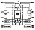
- 듀얼 포트 램의 중재회로에 있어서, 양측 포트의 어드레스 신호로부터 각각 2개의 정, 부 논리신호를 출력하여 어드레스 천이 감지회로(12 및 13)에 입력시키는 2개의 어드레스 버퍼(3 및 5)와, 상기 각각의 정, 부 논리신호중 정논리신호로부터 양측 어드레스 신호의 동일성을 판별하여, 소정수의 신호를 출력하는 소정수의 어드레스 매치 감지회로(11)와, 상기 어드레스 버퍼(3 및 5)의 출력신호로부터 일정시간 지연시켜 각 어드레스 신호에 대응되는 수의 신호를 각각 출력하여 어드레스 천이 조합회로(14 및 16)에 입력시키는 다수의 어드레스 천이 감지회로(12 및 13)와, 상기 어드레스 매치 감지회로(11)의 출력신호를 조합하여 한 개의 출력신호를 생성하여 중재 논리회로(17)에 입력시키는 어드레스 매치 조합회로(15)와, 상기 어드레스 천이 감지회로(12 및 13)의 출력신호를 조합하여 각각 한 개의 출력신호를 생성, 중재논리회로(17)에 입력시키는 어드레스 천이 조합회로(14 및 16)와, 상기 각각의 출력신호로부터 출력을 중재하는 SELECT 신호와 프레그(FLAG) 신호인신호를 출력하는 중재논리회로(17)를 구비하는 것을 특징으로 하는 듀얼 포트 램의 중재회로.

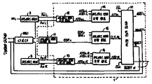
- 제1항에 있어서, 상기 어드레스 매치 감지회로(11)는, 어드레스 신호의 동일성을 판별하기 위하여 배타논리합(EXCLUSIVE OR)회로(G12,G13 및 G14)를 조합하여 조정수로 구성된 것을 특징으로 하는 듀얼 포트 램의 중재회로.
- 제1항에 있어서, 상기 어드레스 천이 감지회로(12 및 13)는, 상기 정, 부 어드레스 버퍼 신호로부터의 출력 신호를 직접 그리고 소정수의 NOT 논리게이트(G3,G4 및 G33) 및 캐패시터(C1 및 C2)로 구성된 지연회로로부터 생성된 지연신호로하여 2개의 NOR게이트(G5 및 G9)에 의해 각각 합성하고 이들 각각의 출력을 한 개의 NOR 게이트(G10)로 합성, NOT 논리게이트(G11)로 반전시켜, 새로운 펄스를 생성함에 의해 어드레스 천이를 감지할 수 있도록 구성한 것을 특징으로 하는 듀얼 포트 램의 중재회로.
- 제1또는 2항에 있어서, 상기 어드레스 매치 조합회로(15)는, 병렬 접속된 다수의 FET(FET4…)에 종속 접속된 2개의 FET(FET5 및 FET6)들로 구성되어, 상기 소정수의 어드레스 매치 감지회로(11)의 출력으로부터 상기 병렬 접속된 다수의 FET들중의 하나 이상의 게이트를 트리거 시킴으로써 상기 종속접속된 FET 접속점에서 정 또는 부 논리 신호가 생성되도록 구성한 것을 특징으로 하는 듀얼 포트 램의 중재회로.
- 제1 또는 3항에 있어서, 상기 어드레스 천이 조합회로(14 및 16)는, 병렬 접속된 다수의 FET(FET1…)들에 종속 접속된 2개의 FET(FET2 및 FET3)들로 구성되어, 상기 어드레스 천이 감지회로(12 및 13)의 출력으로부터 상기 병렬접속된 다수의 FET들중의 하나 이상의 게이트를 트리거시킴으로써 상기 종속접속된 FET 접속점에서 정 또는 부 논리신호가 생성되도록 구성한 것을 특징으로 하는 듀얼 포트 램의 중재회로.
- 제1 또는 5항에 있어서, 상기 중재논리회로(17)에서 우측포트의 어드레스 천이 조합회로(16)의 출력(ATDR) 및 칩 셀렉트신호(R)가 2단의 NOT 게이트(G20 및 G21, G22 및 G23)에 의해 각각 지연되도록 구성하여 동시 신호로 듀얼 포트의 어드레스 및 칩 셀렉트 신호들이 입력되었을 때 항상 좌측포트부처 동작이 허용되는 것을 특징으로하는 듀얼 포트 램의 중재회로.

Priority Applications (1)
| Application Number | Priority Date | Filing Date | Title |
|---|---|---|---|
| KR1019890000744A KR910009552B1 (ko) | 1989-01-25 | 1989-01-25 | 듀얼 포트 램의 중재회로 |
Applications Claiming Priority (1)
| Application Number | Priority Date | Filing Date | Title |
|---|---|---|---|
| KR1019890000744A KR910009552B1 (ko) | 1989-01-25 | 1989-01-25 | 듀얼 포트 램의 중재회로 |
Publications (2)
| Publication Number | Publication Date |
|---|---|
| KR900012269A KR900012269A (ko) | 1990-08-03 |
| KR910009552B1 true KR910009552B1 (ko) | 1991-11-21 |
Family
ID=19283369
Family Applications (1)
| Application Number | Title | Priority Date | Filing Date |
|---|---|---|---|
| KR1019890000744A Expired KR910009552B1 (ko) | 1989-01-25 | 1989-01-25 | 듀얼 포트 램의 중재회로 |
Country Status (1)
| Country | Link |
|---|---|
| KR (1) | KR910009552B1 (ko) |
Families Citing this family (1)
| Publication number | Priority date | Publication date | Assignee | Title |
|---|---|---|---|---|
| KR100360265B1 (ko) * | 2000-10-14 | 2002-11-09 | 엘지전자 주식회사 | 듀얼포트 램의 제어회로 |
-
1989
- 1989-01-25 KR KR1019890000744A patent/KR910009552B1/ko not_active Expired
Also Published As
| Publication number | Publication date |
|---|---|
| KR900012269A (ko) | 1990-08-03 |
Similar Documents
| Publication | Publication Date | Title |
|---|---|---|
| KR100268429B1 (ko) | 동기형반도체메모리장치의데이터의입력회로및데이터입력방법 | |
| US6697926B2 (en) | Method and apparatus for determining actual write latency and accurately aligning the start of data capture with the arrival of data at a memory device | |
| EP0902433B1 (en) | Synchronous dynamic random access memory | |
| KR950004854B1 (ko) | 반도체 메모리 장치 | |
| US7327613B2 (en) | Input circuit for a memory device | |
| JP3317187B2 (ja) | 半導体記憶装置 | |
| JP3645294B2 (ja) | 半導体メモリ装置の多重ビットテスト回路 | |
| EP0744749B1 (en) | Data input circuit of semiconductor storage device | |
| KR19990048133A (ko) | 반도체 메모리 장치의 핀 어사인먼트 방법 및 패킷 단위의 신호를 입력으로 하는 반도체 메모리장치 | |
| KR19980079767A (ko) | 다이나믹형 램 | |
| JPH04322000A (ja) | 半導体記憶装置 | |
| JP4061029B2 (ja) | 半導体メモリ装置、バッファ及び信号伝送回路 | |
| CN100555445C (zh) | 用于读出放大器的半导体存储装置和激活信号产生方法 | |
| KR910009552B1 (ko) | 듀얼 포트 램의 중재회로 | |
| KR930008847A (ko) | 듀얼포트 반도체 기억 장치 | |
| JPH06161870A (ja) | デュアルポートram回路 | |
| US20020031043A1 (en) | Semiconductor memory device | |
| KR100489356B1 (ko) | 단일 스테이지의 멀티플렉서를 가진 메모리 장치의 데이터경로 회로 | |
| JPH08235895A (ja) | 半導体集積回路装置 | |
| KR100213216B1 (ko) | 동기식 반도체 메모리 장치(sdram)를 위한 병렬 비트 테스트(pbt) 제어 회로 및 그 제어 방법 | |
| JPH05307502A (ja) | デュアルポート半導体記憶装置 | |
| US7483320B2 (en) | Data input/output method of semiconductor memory device and semiconductor memory device for the same | |
| SU1741174A1 (ru) | Оперативное запоминающее устройство | |
| JPH0414438B2 (ko) | ||
| US6522181B1 (en) | Semiconductor memory apparatus which can easily attain reduction of access time |
Legal Events
| Date | Code | Title | Description |
|---|---|---|---|
| A201 | Request for examination | ||
| PA0109 | Patent application |
St.27 status event code: A-0-1-A10-A12-nap-PA0109 |
|
| PA0201 | Request for examination |
St.27 status event code: A-1-2-D10-D11-exm-PA0201 |
|
| R17-X000 | Change to representative recorded |
St.27 status event code: A-3-3-R10-R17-oth-X000 |
|
| PG1501 | Laying open of application |
St.27 status event code: A-1-1-Q10-Q12-nap-PG1501 |
|
| E902 | Notification of reason for refusal | ||
| PE0902 | Notice of grounds for rejection |
St.27 status event code: A-1-2-D10-D21-exm-PE0902 |
|
| P11-X000 | Amendment of application requested |
St.27 status event code: A-2-2-P10-P11-nap-X000 |
|
| P13-X000 | Application amended |
St.27 status event code: A-2-2-P10-P13-nap-X000 |
|
| G160 | Decision to publish patent application | ||
| PG1605 | Publication of application before grant of patent |
St.27 status event code: A-2-2-Q10-Q13-nap-PG1605 |
|
| E701 | Decision to grant or registration of patent right | ||
| PE0701 | Decision of registration |
St.27 status event code: A-1-2-D10-D22-exm-PE0701 |
|
| GRNT | Written decision to grant | ||
| PR0701 | Registration of establishment |
St.27 status event code: A-2-4-F10-F11-exm-PR0701 |
|
| PR1002 | Payment of registration fee |
St.27 status event code: A-2-2-U10-U11-oth-PR1002 Fee payment year number: 1 |
|
| PR1001 | Payment of annual fee |
St.27 status event code: A-4-4-U10-U11-oth-PR1001 Fee payment year number: 4 |
|
| PR1001 | Payment of annual fee |
St.27 status event code: A-4-4-U10-U11-oth-PR1001 Fee payment year number: 7 |
|
| PR1001 | Payment of annual fee |
St.27 status event code: A-4-4-U10-U11-oth-PR1001 Fee payment year number: 9 |
|
| PR1001 | Payment of annual fee |
St.27 status event code: A-4-4-U10-U11-oth-PR1001 Fee payment year number: 10 |
|
| PN2301 | Change of applicant |
St.27 status event code: A-5-5-R10-R13-asn-PN2301 St.27 status event code: A-5-5-R10-R11-asn-PN2301 |
|
| PN2301 | Change of applicant |
St.27 status event code: A-5-5-R10-R13-asn-PN2301 St.27 status event code: A-5-5-R10-R11-asn-PN2301 |
|
| PR1001 | Payment of annual fee |
St.27 status event code: A-4-4-U10-U11-oth-PR1001 Fee payment year number: 11 |
|
| PR1001 | Payment of annual fee |
St.27 status event code: A-4-4-U10-U11-oth-PR1001 Fee payment year number: 12 |
|
| PR1001 | Payment of annual fee |
St.27 status event code: A-4-4-U10-U11-oth-PR1001 Fee payment year number: 13 |
|
| PR1001 | Payment of annual fee |
St.27 status event code: A-4-4-U10-U11-oth-PR1001 Fee payment year number: 14 |
|
| PR1001 | Payment of annual fee |
St.27 status event code: A-4-4-U10-U11-oth-PR1001 Fee payment year number: 15 |
|
| PR1001 | Payment of annual fee |
St.27 status event code: A-4-4-U10-U11-oth-PR1001 Fee payment year number: 16 |
|
| FPAY | Annual fee payment |
Payment date: 20071025 Year of fee payment: 17 |
|
| PR1001 | Payment of annual fee |
St.27 status event code: A-4-4-U10-U11-oth-PR1001 Fee payment year number: 17 |
|
| LAPS | Lapse due to unpaid annual fee | ||
| PC1903 | Unpaid annual fee |
St.27 status event code: A-4-4-U10-U13-oth-PC1903 Not in force date: 20081122 Payment event data comment text: Termination Category : DEFAULT_OF_REGISTRATION_FEE |
|
| PC1903 | Unpaid annual fee |
St.27 status event code: N-4-6-H10-H13-oth-PC1903 Ip right cessation event data comment text: Termination Category : DEFAULT_OF_REGISTRATION_FEE Not in force date: 20081122 |
|
| PN2301 | Change of applicant |
St.27 status event code: A-5-5-R10-R13-asn-PN2301 St.27 status event code: A-5-5-R10-R11-asn-PN2301 |
|
| PN2301 | Change of applicant |
St.27 status event code: A-5-5-R10-R13-asn-PN2301 St.27 status event code: A-5-5-R10-R11-asn-PN2301 |
|
| PN2301 | Change of applicant |
St.27 status event code: A-5-5-R10-R13-asn-PN2301 St.27 status event code: A-5-5-R10-R11-asn-PN2301 |
|
| P22-X000 | Classification modified |
St.27 status event code: A-4-4-P10-P22-nap-X000 |