KR910009552B1 - Arbiter of dual port ram - Google Patents

Arbiter of dual port ram Download PDF

Info

Publication number
KR910009552B1
KR910009552B1 KR1019890000744A KR890000744A KR910009552B1 KR 910009552 B1 KR910009552 B1 KR 910009552B1 KR 1019890000744 A KR1019890000744 A KR 1019890000744A KR 890000744 A KR890000744 A KR 890000744A KR 910009552 B1 KR910009552 B1 KR 910009552B1
Authority
KR
South Korea
Prior art keywords
address
circuit
signal
signals
logic
Prior art date
Legal status (The legal status is an assumption and is not a legal conclusion. Google has not performed a legal analysis and makes no representation as to the accuracy of the status listed.)
Expired
Application number
KR1019890000744A
Other languages
Korean (ko)
Other versions
KR900012269A (en
Inventor
한광마
Original Assignee
현대전자산업 주식회사
정몽헌
Priority date (The priority date is an assumption and is not a legal conclusion. Google has not performed a legal analysis and makes no representation as to the accuracy of the date listed.)
Filing date
Publication date
Application filed by 현대전자산업 주식회사, 정몽헌 filed Critical 현대전자산업 주식회사
Priority to KR1019890000744A priority Critical patent/KR910009552B1/en
Publication of KR900012269A publication Critical patent/KR900012269A/en
Application granted granted Critical
Publication of KR910009552B1 publication Critical patent/KR910009552B1/en
Expired legal-status Critical Current

Links

Images

Classifications

    • GPHYSICS
    • G11INFORMATION STORAGE
    • G11CSTATIC STORES
    • G11C11/00Digital stores characterised by the use of particular electric or magnetic storage elements; Storage elements therefor
    • G11C11/21Digital stores characterised by the use of particular electric or magnetic storage elements; Storage elements therefor using electric elements
    • G11C11/34Digital stores characterised by the use of particular electric or magnetic storage elements; Storage elements therefor using electric elements using semiconductor devices
    • CCHEMISTRY; METALLURGY
    • C07ORGANIC CHEMISTRY
    • C07CACYCLIC OR CARBOCYCLIC COMPOUNDS
    • C07C21/00Acyclic unsaturated compounds containing halogen atoms
    • C07C21/02Acyclic unsaturated compounds containing halogen atoms containing carbon-to-carbon double bonds
    • C07C21/18Acyclic unsaturated compounds containing halogen atoms containing carbon-to-carbon double bonds containing fluorine

Landscapes

  • Chemical & Material Sciences (AREA)
  • Organic Chemistry (AREA)
  • Engineering & Computer Science (AREA)
  • Computer Hardware Design (AREA)
  • Static Random-Access Memory (AREA)

Abstract

The circuit, when a left and a right port select same memory cell to read or to write, allows RAM operation of one port and prevents the other port to access the memory cell during that period. The circuit includes address buffers (3,5) for generating two logic signals from the address signals and for transmitting to address transition detecting circuits (12,13), an address matching detection circuit (11) for discriminating the identity of address signals of two ports by checking the positive logic signal, address transition detecting circuit (12,13) for generating the signals which number is matched with the number of address signals and for transmitting to address transition combining circuits (14,16), and an address match combining circuit (15) for generating one signal by combining the output signals of the address match detection circuit (11).

Description

듀얼 포트 램의 중재회로Dual port RAM arbitration circuit

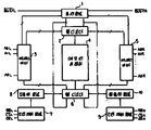
제1도는 듀얼 포트 램의 블럭도.1 is a block diagram of a dual port RAM.

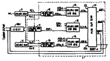
제2도는 본 발명에 따른 중재회로의 블럭도.2 is a block diagram of an arbitration circuit according to the present invention.

제3도는 제3도의 상세회로도.3 is a detailed circuit diagram of FIG.

제4a도 내지 제4d도는 본 발명에 따른 중재회로의 동작설명을 위한 타이밍도.4a to 4d are timing diagrams for explaining the operation of the arbitration circuit according to the present invention.

* 도면의 주요부분에 대한 부호의 설명* Explanation of symbols for the main parts of the drawings

1 : 중재회로 2 : 열디코더1: Arbitrary Circuit 2: Thermal Decoder

3 및 5 : 어드레스버퍼 4 : 메모리 어레이3 and 5: address buffer 4: memory array

6 : 행디코더 7 및 9 : 논리제어회로6: row decoder 7 and 9: logic control circuit

8 및 10 : 입출력회로 11 : 어드레스 매치 감지회로8 and 10: input / output circuit 11: address match detection circuit

12 및 13 : 어드레스 천이 감지회로 15 : 어드레스 매치 조합회로12 and 13: address transition detection circuit 15: address match combination circuit

14 및 16 : 어드레스 천이 조합회로 17 : 중재논리회로14 and 16: address transition combination circuit 17: arbitration logic circuit

본 발명은 듀얼 포트 램(DUAL PORT RAM)이 중재(ARBITRATION)회로에 관한 것으로, 특히 램 동작중 우측포트와 좌측포트, 즉 양포트가 동일위치의 동일 메모리 셀을 선택하여 동시에 서입 또는 판독하려고 할때, 어느 한쪽 포트의 램동작을 허용하고 다른쪽 포트는 그 기간 동안 동일 셀에 대한 램동작이 금지되도록 구성한 신규의 듀얼 포트 램의 중재회로에 관한 것이다.The present invention relates to a dual bit RAM (ARBITRATION) circuit, and in particular, the right port and the left port, that is, both ports select the same memory cell at the same position to write or read at the same time during RAM operation. At this time, it relates to the arbitration circuit of a new dual port RAM configured to allow the RAM operation of one port and the other port is prohibited from the RAM operation for the same cell during that period.

일반적으로 듀얼 포트 램(DUAL PORT RAM)은 같은 메모리 용량을 놓고 좌측포트와 우측포트, 즉 듀얼 포트에서 서입(WRITE) 및 판독(READ) 동작이 동시에 가능하도록 하자는 견지에서 설계되고 개발되었다. 이러한 듀얼 포트에서의 램동작은 각 포트가 메모리 어레이(MEMORY ARRAY)중에서 서로 다른 메모리 셀(MEMORY CELL)을 선택했을 때 가능한 것으로 만약에 램동작중 양포트가 같은 위치의 동일 메모리 셀을 선택하여 동시에 서입 또는 판독을 하려고 하는 경우 일정한 원칙에 의해 한쪽 포트만이 램동작이 허용되고 다른쪽 포트는 그 기간동안 동일셀에 대한 램동작이 금지되는 중재회로(ARBITRATION CIRCUITS)가 필요하다.In general, dual port RAM is designed and developed in the sense that both write and read operations can be simultaneously performed on the left port and the right port, that is, the dual port, with the same memory capacity. The RAM operation in this dual port is possible when each port selects a different memory cell in the memory array. If both ports select the same memory cell at the same location during the RAM operation, In the case of writing or reading, a certain principle requires an ARBITRATION CIRCUITS where only one port is allowed to operate the RAM and the other port is prohibited from operating the same cell during that period.

본 발명은 듀얼 포트 램의 중재회로에 관한 것으로서 다음의 세가지 논리원칙에 의해 동일셀에 대한 듀얼 포트의 램동작을 조정 중재한다.The present invention relates to an arbitration circuit of dual port RAM, and arbitrates the arbitration of dual port RAM operation for the same cell by the following three logic principles.

첫번째 논리 원칙은 일정셀에 대한 어드레스(ADDRESS)선택이 먼저 이루어진 포트를 동작이 허용되도록 하고, 동작이 허용된 포트가 일정셀에 대해 램동작을 하고 있는 시간동안은 다른쪽 포트로부터의 동일셀에 대한 램동작을 금지하는 어드레스 중재논리회로이다.The first logic principle is to allow the operation of the port where the address selection for a certain cell is made first, and to the same cell from the other port during the time that the allowed port is doing RAM operation for the certain cell. This is an address arbitration logic circuit that prohibits RAM operation.

둘째는 칩 셀렉트(CHIP SELECT)중재논리로서 듀얼 포트의 어드레스가 이미 동일 셀 선택을 위해 매치(MATCH)가 된 상태(양 포트의 어드레스가 같은 상태)에서 양포트의 칩 셀렉트 신호가 먼저 인에이블(ENABLE)된 포트가 동작이 허용되고 다른쪽 포트는 그 시간동안 동일셀에 대한 동작이 금지되는 논리원칙이다.The second is the chip select arbitration logic, in which the chip select signals of both ports are enabled first when the address of the dual port is already matched for the same cell selection (the address of both ports are the same). The ENABLE) port is allowed to operate, and the other port is the logic principle that operation for the same cell is prohibited during that time.

셋째는 양포트로부터의 어드레스 또는 칩 셀렉트 신호가 상기 어드레스 중재논리와 칩 셀렉트 중재논리, 두 논리에 의해 구별될 수 없는 동시신호로 입력되었을 때 항상 좌측포트의 동작을 허용하고 우측포트는 그 시간동안 동일 셀에 대한 동작을 금지하는 동시신호 중재논리이다.Thirdly, when the address or chip select signal from both ports is inputted simultaneously with the signal arbitration logic and the chip select arbitration logic, the left port always permits the operation of the left port and the right port during that time. Simultaneous signal arbitration logic that prohibits operation for the same cell.

따라서, 본 발명은 듀얼 포트 램의 중재회로가 상기 세가지 중재논리원칙을 구현하면서 중재논리가 성립 또는 해제되었을때의 프래그(FLAG) 신호인

Figure kpo00001
의 응답시간을 신속하게 하여 CPU가 이를 감지하는 시간을 종전보다 빠르게 개선하였고 안정된 동작을 제공하는데 그 목적이 있다.Accordingly, the present invention is a FLAG signal when the arbitration logic is established or released while the arbitration circuit of the dual port RAM implements the above three arbitration logic principles.
Figure kpo00001
Its purpose is to improve the response time of the CPU faster than before, and to provide stable operation.

본 발명의 듀얼 포트 램의 중재회로에 의하면 상기 중재논리원칙과

Figure kpo00002
의 빠른 응답시간, 안정된 중재회로 동작을 구현하기 위해 다음과 같은 특징적인 논리회로 및 구성으로 설계된다. 즉 동일셀에 대한 어드레스의 선택이 어느쪽 포트부터 일어났는지를 판별하기 위해서 각 포트의 모든 어드레스 버퍼(ADDRESS BUFFER)에 어드레스 천이감지회로(ADDRESS TRANSITION DETECTION CIRCUIT)를 연결 사용하고, 모든 어드레스 천이감지회로의 출력들은 어드레스 천이조합회로를 통해 각 포트별로 조합되어 하나의 클럭씩(CLOCK, ATDL, ATDR)을 만들고 이를 중재논리회로에 인가한다. 또한 양포트의 어드레스가 동일셀 선택을 위해서 같은 논리신호가 되었는지를 판별하기 위해 양포트의 어드레스 버퍼의 정신호 출력들을(An L, An R) 입력으로 하는 어드레스 매치감지회로(EXCLUSIVE OR FUNCTION)를 채택하고, 각 어드레스 매치감지회로의 출력들을 입력으로 하는 어드레스 매치조합회로를 통해 모든 어디레스가 동일한지 여부를 클럭(CLK AL)으로 만들어 중재논리회로에 인가한다. 각포트의 어드레스 천이 조합회로의 출력들과 어드레스 매치조합회로의 출력, 각포트의 칩 셀렉트 신호의 출력(CS L, CS R)들을 입력으로 하는 중재논리회로는 상기 세가지 중재 논리원칙에 따라 동일셀에 대한 듀얼포트의 램동작을 중재하며
Figure kpo00003
L와
Figure kpo00004
R 신호를 출력으로 하여 CPU가 이를 감지할 수 있도록 한다.According to the arbitration circuit of the dual port RAM of the present invention,
Figure kpo00002
In order to realize fast response time and stable arbitration circuit operation, it is designed with the following characteristic logic circuit and configuration. In other words, in order to determine from which port the address selection for the same cell occurs, the address transition detection circuit is used to connect all address buffers of each port to the address buffer. The outputs of are combined by each port through the address transition combination circuit to make one clock (CLOCK, ATDL, ATDR) and apply it to the arbitration logic circuit. In addition, an address match detection circuit (EXCLUSIVE OR FUNCTION) is adopted to input the positive signal outputs (An L, An R) of the address buffers of both ports to determine whether the addresses of both ports are the same logic signal for selecting the same cell. Then, through the address match combination circuit which inputs the outputs of the respective address match detection circuits, the clock CLK AL is applied to the arbitration logic circuit to determine whether all addresses are the same. Arbitrary logic circuits that input the outputs of the address transition combination circuits of each port, the outputs of the address match combination circuits, and the outputs (CS L, CS R) of the chip select signals of each port are the same To mediate the dual port RAM operation
Figure kpo00003
L and
Figure kpo00004
The R signal is output so that the CPU can detect it.

이하, 첨부된 도면을 참조하여 본 발명을 상세히 설명하기로 한다.Hereinafter, with reference to the accompanying drawings will be described in detail the present invention.

제1도는 일반적인 듀얼 포트 램을 설명하기 위한 블록도로서, Ao L 내지 An L의 좌측 포트 어드레스 신호 및 Ao R 내지 An R의 우측포트 어드레스 신호가 어드레스 버퍼(3 및 5)에 각기 인가되어, 이 인가된 신호들을 정신호 및 부신호(예를 들어 Ao 및

Figure kpo00005
)로 변환시키는 상기 어드레스 버퍼(3 및 5)는 메모리 어레이(4)를 선택하기 위한 열디코더(2)와 행디코더(6) 그리고 이 열, 행디코더(2 및 6)를 인에이블(ENABLE)하기 위한 중재회로(1)에 각각 접속된다. 이 중재회로(1)는 다시 상기 열, 행디코더(2 및 6)를 통해 상기 메모리 어레이에 접속된다.1 is a block diagram illustrating a general dual port RAM, in which left port address signals of Ao L to An L and right port address signals of Ao R to An R are applied to the address buffers 3 and 5, respectively. The applied signals may be applied to the positive signal and the sub signal (e.g., Ao and
Figure kpo00005
The address buffers 3 and 5, which are converted into a plurality of columns, enable the column decoder 2 and the row decoder 6 for selecting the memory array 4, and the columns and the row decoders 2 and 6. It is connected to the arbitration circuit 1 for each. This arbitration circuit 1 is in turn connected to the memory array via the column, row decoders 2 and 6.

또한 논리제어회로(7 및 9)는 칩의 동작 또는 정지 상태를 제어하는

Figure kpo00006
신호, 칩의 판독 또는 서입상태를 제어하는
Figure kpo00007
신호, 판독된 데이터를 출력시키는 상태를 조정하는
Figure kpo00008
신호로 구성되어, 각 포트의 논리제어 회로는 입출력회로(8 및 10)를 제어한다. 동일셀에 대한 양포트의 선택이 이루어지는 경우와 보통 상태의 칩 동작의 경우는 중재회로(1)의 출력인
Figure kpo00009
L 및
Figure kpo00010
R 신호상태로 판별할 수 있다.The logic control circuits 7 and 9 also control the operation or stop state of the chip.
Figure kpo00006
To control the reading or writing of signals, chips
Figure kpo00007
Signal, to adjust the state to output the read data
Figure kpo00008
Consists of a signal, the logic control circuit of each port controls the input / output circuits 8 and 10. In the case of selecting both ports for the same cell and in the case of normal chip operation, the output of the arbitration circuit 1
Figure kpo00009
L and
Figure kpo00010
It can be determined by the R signal state.

제2도는 상술한

Figure kpo00011
제어신호 처리를 신속 정확하게 하기 위해 본 발명에 따라 새로이 구성된 상기 듀얼 포트 램의 중재회로(1)의 블록도로서, Ao 내지 An까지의 어드레스 신호중 An신호만을 발췌하여 설명하기로 한다. 여기서 첨자 L은 좌측 포트 그리고 R은 우측 포트를 의미한다.2 is described above.
Figure kpo00011
As a block diagram of the arbitration circuit 1 of the dual port RAM newly configured according to the present invention to quickly and accurately control the control signal, only An signal from the address signals Ao to An will be described. Where the subscript L is the left port and R is the right port.

먼저, 좌,우측 포트의 어드레스 신호 An L 및 An R 신호가 양포트의 어드레스 버퍼(3 및 5)에 인가되면 이 어드레스 버퍼(3 및 5)는

Figure kpo00012
L, An L 및
Figure kpo00013
R, An R 신호를 생성하여, 이들 신호들을 어드레스 천이 감지회로(12 및 13) 및 열, 행디코더(2 및 6)에 인가시킨다. 또한, 상기 An L 및 An R 신호는 어드레스 매치 감지회로(11)에 인가되어 이 회로(11)에서 An L
Figure kpo00014
An R 신호인 EoRn 신호(실제로는 EoRo,EoR1,EoR2…EoR7임)를 생성하여 어드레스 매치 조합회로(15)에 인가시킨다. 그리하여, 상기 어드레스 매치 조합회로(15)에서는 상기 EOR 신호들을 조합하여 한 개의 클럭펄스 CLK AL 신호를 생성하여 중재논리회로(17)에 인가시킨다.First, when the address signals An L and An R signals of the left and right ports are applied to the address buffers 3 and 5 of both ports, the address buffers 3 and 5
Figure kpo00012
L, An L and
Figure kpo00013
R and An R signals are generated and applied to the address transition detection circuits 12 and 13 and the column and row decoders 2 and 6. In addition, the An L and An R signals are applied to the address match detection circuit 11, whereby An L
Figure kpo00014
An EoRn signal (actually EoRo, EoR1, EoR2 ... EoR7), which is an An R signal, is generated and applied to the address match combination circuit 15. Thus, the address match combination circuit 15 combines the EOR signals to generate one clock pulse CLK AL signal and applies it to the arbitration logic circuit 17.

한편, 상기 어드레스 천이 감지회로(12 및 13)에서는 상기 어드레스 버퍼(3 및 5)에서 각각 출력되는 2개의 신호를 일정시간지연, 변환하여 ATD 신호(실제로는 ATDo,ATD1,ATD2…TDn)를 생성하고, 이 신호들(ATDn L 및 ATDn R)을 어드레스 천이 조합회로(14 및 16)에 인가시키면, 이 회로(14 및 16)에서는 인가된 신호들을 조합하여 ATD L 및 ATD R 신호를 생성한다음, 이 신호들(ATD L 및 ATD R)을 상기 중재 논리회로(17)에 인가시킨다.Meanwhile, the address transition detection circuits 12 and 13 delay and convert two signals output from the address buffers 3 and 5, respectively, to generate ATD signals (actually ATDo, ATD1, ATD2, ... TDn). When the signals ATDn L and ATDn R are applied to the address transition combination circuits 14 and 16, the circuits 14 and 16 combine the applied signals to generate ATD L and ATD R signals. These signals ATD L and ATD R are applied to the arbitration logic circuit 17.

상기 중재 논리회로(17)에서는 상술한 신호들의 인가에 따라 SELEET 및

Figure kpo00015
출력단자에 논리적 “고” 또는 “저” 신호가 출력되는데,
Figure kpo00016
출력은 마이크로 프로세서의 CPU 동작을 제어하는데 이용되고, 셀렉트 단자 출력은 상기 열, 행디코더(2 및 6)에 접속되어, 이 디코더(2 및 6)의 동작을 제어하게 된다.In the arbitration logic circuit 17, SELEET and
Figure kpo00015
Logical “high” or “low” signal is output to the output terminal.
Figure kpo00016
The output is used to control the CPU operation of the microprocessor, and the select terminal output is connected to the column, row decoders 2 and 6 to control the operation of the decoders 2 and 6.

제3도는 제2도의 상세 회로도로서, 좌측 포트의 어드레스 신호 An L은 NOT 논리게이트 G1 및 G2를 경유한 An L 신호와 NOT 논리게이트 G6를 경유한

Figure kpo00017
L 신호로 분리되는데, 전자인 상기 An L 신호는 직접 그리고 NOT 논리게이트 G3, G4 및 G33 그리고 이들 사이에 접지된 캐패시터 C1 및 C2로 구성된 지연회로를 경유해 NOR 게이트 G5에 입력되고, 후자인
Figure kpo00018
L 신호는 직접 그리고 NOT 논리게이트 G7, G8 및 G34 그리고 이들사이에 접지된 캐패시터 C3 및 C4로 구성된 지연회로를 경유해 NOR 게이트 G9에 각각 입력된다.3 is a detailed circuit diagram of FIG. 2, in which the address signal An L of the left port passes through the An L signal via NOT logic gates G1 and G2 and the NOT logic gate G6.
Figure kpo00017
The An L signal, which is the former, is input to the NOR gate G5 directly and via a delay circuit composed of NOT logic gates G3, G4 and G33 and grounded capacitors C1 and C2 therebetween.
Figure kpo00018
The L signal is input to the NOR gate G9, respectively, directly and via a delay circuit consisting of NOT logic gates G7, G8 and G34, and capacitors C3 and C4 grounded therebetween.

따라서, 상기 NOR 게이트 G5 및 G9의 각각의 출력은 NOR 게이트 G10을 경유해 NOT 게이트 G11에서 반전되어 ATDn 펄스가 생성된다(본 명세서에서는 편의상 하나의 ATDn 펄스 생성과정만 세술하고 있지만, 실제로는 상술한 회로가 여러개 나열되어 ATD1, ATD2, ATD3…ATDn 펄스가 생성된다). 상기 ATDn 펄스신호가 FET1의 게이트 단자에 인가되는데, 이 펄스신호가 High 상태(즉 어드레스 천이가 일어난 상태)이면 FET1이 ON되고 칩 셀렉터 신호의 CSL.CSR가 논리적으로 High 상태에서 FET2와 FET3의 접속점은 노리적으로 LOW 상태가 된다. 이상태가 NOT 게이트 G15에서 반전되어 NOR 게이트 G18의 한 입력단자에 인가된다.Therefore, the respective outputs of the NOR gates G5 and G9 are inverted at the NOT gate G11 via the NOR gate G10 to generate an ATDn pulse. Multiple circuits are listed, generating ATD1, ATD2, ATD3… ATDn pulses). The ATDn pulse signal is applied to the gate terminal of the FET1. When the pulse signal is high (that is, the address transition has occurred), the FET1 is turned on and the connection point of the FET2 and the FET3 when the CSL.CSR of the chip selector signal is logically high. Is logically LOW. This state is inverted at the NOT gate G15 and applied to one input terminal of the NOR gate G18.

한편, 우측 포트의 어드레스 신호 An R 또한 상술한 좌측 포트의 어드레스 신호 An L 전달과정과 동일한 동작으로, 어드레스 버퍼(5), 어드레스 천이 감지회로(13)를 거쳐 어드레스 천이 조합회로(16)에서의 NOT 게이트 G35의 출력이 시간지연을 위한 NOT 게이트 G22 및 G23을 경유해 NOR 게이트 G19의 한입력 단자에 인가된다. 여기서 상술한 우측 포트측의 어드레스 버퍼(5), 어드레스 천이 감지회로(13) 및 어드레스 천이 조합회로(16)의 구성은 좌측 포트 측의 회로와 구성이 동일하므로 그 설명은 생략키로 한다.On the other hand, the address signal An R of the right port is also the same operation as that of the address signal An L of the left port described above, and the address transition combination circuit 16 passes through the address buffer 5 and the address transition detection circuit 13. The output of NOT gate G35 is applied to one input terminal of NOR gate G19 via NOT gates G22 and G23 for time delay. The configuration of the address buffer 5, the address transition detection circuit 13, and the address transition combination circuit 16 on the right port side described above is the same as the circuit on the left port side, and a description thereof will be omitted.

상술한 양측의 어드레스 버퍼(3 및 5)에서 출력되는 신호중 An L 및 An R 신호를 게이트 G12, G13 및 G14로 구성된 배타 논리합(EXCLUSIVE OR)(11)회로에 인가시켜, 이 두 개의 신호가 다를때만 NOR 게이트 G14에서 High 신호가 출력되는 EoRn(실제로는 상기 배타 논리합 회로가 수개로 구성되어 EoR1,EoR2,EoR3…EoRn의 펄스신호가 된다) 펄스신호를 생성하여, EoRn 펄스 신호를 FET4의 게이트에 인가시키면 이펄스신호에 따라 상기 FET4가 ON 또는 OFF 되고 칩 셀렉터 신호를 조합한

Figure kpo00019
신호에 따라 FET6과 FET5의 접속점의 상태가 변환된다음, NOT 논리게이트 G16를 거쳐 CLK AL 펄스 신호를 생성하여 역시 NOT 논리게이트 G17를 거쳐 중재논리회로(17)의 FET10, FET7, FET8, FET9의 게이트 단자에 인가되고 또한 CLK AL 신호는 직접 NOR 게이트 G24, G35에 연결된다.Among the signals output from the address buffers 3 and 5 described above, An L and An R signals are applied to an exclusive OR 11 circuit composed of gates G12, G13 and G14, so that these two signals are different. Only when the high signal is output from the NOR gate G14 (actually, the exclusive OR circuit is composed of several excitation pulse signals of EoR1, EoR2, EoR3… EoRn) to generate a pulse signal, and sends the EoRn pulse signal to the gate of FET4. When applied, the FET4 is turned on or off according to this pulse signal, and the chip selector signal is combined.
Figure kpo00019
According to the signal, the state of the connection point of FET6 and FET5 is converted, and then generates a CLK AL pulse signal through the NOT logic gate G16, and also through the NOT logic gate G17, It is applied to the gate terminal and also the CLK AL signal is directly connected to the NOR gates G24 and G35.

상술한 바와 같이, 중재논리회로(17)에 인가된 상기 신호들에 따라 좌측 포트 또는 우측 포트가 선택되는데, 이 동작 설명은 제4a도 내지 제4d도에 도시된 타이밍도를 참조하여 상세히 설명하면 다음과 같다.As described above, the left port or the right port is selected according to the signals applied to the arbitration logic circuit 17. This operation description will be described in detail with reference to the timing diagrams shown in Figs. 4A to 4D. As follows.

CLK AL 신호가 HIGH 상태인 경우, 즉 각 포트의 어드레스들이 동일 논리신호가 아닌 상태여서 동일셀에 대한 각 포트의 동작이 이루어지지 않는 보통상태의 듀얼 포트 램동작에서는 제3도의 중재논리회로(17)의 G24와 G35의 출력들은 다른쪽 입력(점 A와 점 B)의 상태와는 관계없이 CLK AL에 의해 결정되므로 NOR 게이트 G24와 G35의 출력신호는 LOW이다. 두단의 NOT 논리게이트를 거친 신호 역시 LOW이므로 FET16, FET17, FET19, FET20은 OFF 상태이고 FET15, FET18은 ON 상태이다. 따라서

Figure kpo00020
L,
Figure kpo00021
R은 HIGH 상태로 있으며 디코더의 출력인 SELECT L 및 SELECT R도 변화가 없이 각 포트별로 보통 램동작을 계속하게 된다. 이와 같이 중재논리회로의 중재가 필요하지 않아 보통상태를 유지하고 있는 시간은 타이밍도(제4a도 내지 제4d도)에서 T1 이전 구간과 T2부터 T3까지 구간, T4이후의 구간을 가리킨다. 제4a도와 제4b도는 상기에서 기술한 어드레스 중재논리에 의한 타이밍도로서 좌측포트와 우측포트의 우선순위에 따른 경우의 수를 도시한 것이다. 제4c도와 제4d도는 칩 셀렉트 중재논리에 의한 타이밍도를 역시 나타낸 것이다.When the CLK AL signal is HIGH, that is, in the normal dual port RAM operation in which the ports of the respective ports are not the same logic signal and the operation of each port for the same cell is not performed, the arbitration logic circuit of FIG. The output signals of NOR gates G24 and G35 are LOW because the outputs of G24 and G35 of the N2) are determined by CLK AL regardless of the state of the other inputs (points A and B). Since the signal through the two NOT logic gates is also LOW, FET16, FET17, FET19, and FET20 are OFF and FET15 and FET18 are ON. therefore
Figure kpo00020
L,
Figure kpo00021
R is HIGH and the decoder's outputs, SELECT L and SELECT R, remain unchanged and continue to operate normally for each port. As such, the time that the mediation logic does not require mediation and maintains the normal state indicates a section before T1, a section from T2 to T3, and a section after T4 in the timing diagrams (FIGS. 4A to 4D). 4A and 4B are timing diagrams based on the address arbitration logic described above, and show the number of cases in accordance with the priority of the left port and the right port. 4C and 4D also show timing diagrams based on chip select arbitration logic.

먼저, 제4a도의 경우를 제3도의 회로와 함께 설명하여 보기로 한다.First, the case of FIG. 4A will be described together with the circuit of FIG.

CLK AL T1에서 LOW 상태로 바뀌면, 즉 각 포트의 어드레스들이 동일셀 선택을 위해 동일 논리신호가 되면 어드레스 매치회로와 어드레스 매치조합회로를 거쳐 G24와 G35의 CLK AL 입력은 LOW 상태가되므로 앞단의 ATD 신호와

Figure kpo00022
신호에 의해 결정되는 G24와 G35의 다른쪽 입력(점 A와 점 B)에 의해 출력의 상태가 좌우된다. ATD L 신호는 상기에서 기술한 어드레스 버퍼, 어드레스 감지회로, 어드레스 감지조합회로를 거쳐 T1에서 CLK AL의 변환점과 앞뒤로 겹치는 클럭을 생성한다. CLK AL G17를 거텨 HIGH 상태가 되어 FET10, FET9는 OFF되고 FET7, FET8, FET8, FET12, FET13은 ON된다.When CLK AL T1 is changed to LOW state, that is, when the address of each port becomes the same logic signal for selecting the same cell, the CLK AL input of G24 and G35 goes through the address match circuit and the address match combination circuit, so the ATD Signal and
Figure kpo00022
The state of the output depends on the other input (points A and B) of G24 and G35, which are determined by the signal. The ATD L signal generates a clock that overlaps with the conversion point of CLK AL back and forth at T1 through the address buffer, address sensing circuit, and address sensing combination circuit described above. It goes high through CLK AL G17, FET10 and FET9 are turned off and FET7, FET8, FET8, FET12 and FET13 are turned on.

T1시점에서 볼 때 ATD L 은 HIGH 상태이므로 G18과 FET17을 거쳐 점 A의 상태는 LOW이고, ATD R과

Figure kpo00023
R이 모두 LOW인 상태에서 G19의 출력은 HIGH이므로 FET8을 거친 점 B의 HIGH 상태, FET12와 FET11을 거쳐 점 A를 계속 LOW 상태로 유지시킨다. 따라서 G24의 출력은 HIGH 상태, G25와 G26, G27과 G28을 거친 출력 역시 HIGH이므로 FET16은 ON, FET15는 OFF되어
Figure kpo00024
L이 LOW상태로 바뀐다. 또한 FET17이 ON되어 디코더의 출력인 SELECT L을 LOW로 바꾸어 결국 좌측 포트는 우측포트가 먼저 선택한 동일 메모리셀을 선택하지 못한다. 반면 점 B의 상태는 계속 HIGH이므로 좌측 포트와는 관계없이 우측포트는 선택한 메모리셀에 대한 램동작을 계속할 수 있다.At the time of T1, ATD L is HIGH, so point A is LOW through G18 and FET17, and ATD R and
Figure kpo00023
The output of G19 is HIGH when R is all LOW, so point A remains LOW through FET8 HIGH, FET12 and FET11. Therefore, the output of G24 is HIGH, and the output through G25 and G26, G27 and G28 is HIGH, so FET16 is ON and FET15 is OFF.
Figure kpo00024
L changes to LOW state. In addition, FET17 is turned ON, which changes the output of the decoder, SELECT L, to LOW, so that the left port cannot select the same memory cell selected by the right port first. On the other hand, since the state of point B remains HIGH, the right port can continue the RAM operation for the selected memory cell regardless of the left port.

상기의 중재논리에 의해 이루어진 신호들의 상태는 T2시점에서 우측포트의 어드레스가 바뀌어 CLK AL이 HIGH 상태로 되면 해제된다. 즉

Figure kpo00025
L과 SELECT L이 HIGH 상태로 돌아오고 우측포트가 선택했던 메모리 셀에 대해 좌측포트가 램동작을 수행할 수 있으며 우측포트는 다른 위치의 메모리셀을 선택, 동작을 한다.The state of the signals made by the arbitration logic is canceled when the address of the right port is changed at the time T2 and the CLK AL becomes HIGH. In other words
Figure kpo00025
L and SELECT L return to the HIGH state, and the left port can perform RAM operation on the memory cell selected by the right port, and the right port selects and operates the memory cell at another position.

T3에서 T4 구간의 타이밍도는 T1에서 T2구간에서 발생한 경우를 좌측, 우측포트끼리 서로 바뀌어 놓은 상황과 같다. 즉 T3시점에서 볼 때 ATD R은 HIGH 상태이므로 G19와 FET8을 거친 점 B의 상태는 LOW이고 ATD L과

Figure kpo00026
L이 모두 LOW인 상태에서 G18의 출력은 HIGH이므로 FET7을 거친 점 A의 HIGH 상태는 FET13과 FET14를 거쳐 점 B를 계속 LOW 상태로 유지시킨다. 따라서 G35의 출력은 HIGH 상태, G29와 G30, G31과 G32를 거친 출력 역시 HIGH이므로 FET19는 ON, FET18은 OFF되어
Figure kpo00027
R이 LOW 상태로 바뀐다. 또한 FET20이 ON되어 디코더의 출력인 SELECT R을 LOW로 바뀌어 결국 우측포트는 좌측포트가 먼저 선택한 동일 메모리셀을 선택하지 못한다. 반면 점 A의 상태는 계속 HIGH이므로 우측포트와는 관계없이 좌측포트는 선택한 메모리셀에 대한 램동작을 계속하고 T4시점에서 중재논리가 해제되어 양포트는 서로 다른 메모리셀을 선택하게 되므로 보통의 듀얼 포트 램 동작 상태로 넘어오게 된다.The timing diagram of the T3 to T4 section is the same as the situation where the left and right ports are interchanged with each other when the T1 to T2 section occurs. That is, ATD R is HIGH at the time of T3, so the state of point B passing through G19 and FET8 is LOW and ATD L and
Figure kpo00026
The output of G18 is high when L is all low, so the high state of point A through FET7 keeps point B low through FET13 and FET14. Therefore, the output of G35 is HIGH, and the output through G29 and G30, G31 and G32 is also HIGH, so FET19 is ON and FET18 is OFF.
Figure kpo00027
R changes to LOW state. In addition, the FET20 is turned on, and the output of the decoder, SELECT R, is changed to LOW. Therefore, the right port cannot select the same memory cell selected by the left port first. On the other hand, since the state of point A is still HIGH, the left port continues the RAM operation for the selected memory cell irrespective of the right port, and arbitration logic is released at T4, so both ports select different memory cells. The port will enter the operating state.

제4b도 역시 어드레스 중재논리의 또 다른 경우의 타이밍도를 나타낸 것으로 제4a도의 경우에서 설명한 바와 같은 중재논리회로의 동작으로 실행되며 중재논리가 성립되는 경우의 차이점을 설명하여 보면 다음과 같다.FIG. 4B also shows another timing diagram of the address arbitration logic, which is executed by the operation of the arbitration logic circuit as described in the case of FIG. 4A, and the difference between the case where the arbitration logic is established is as follows.

제4a도의 경우 T1이전 구간에서 우측포트가 일정셀에 대해 동작을 하고 있는 상황에서 우측포트가 선택하고 있는 동일셀에 대해 좌측포트가 동작을 하기 위한 상태로 바뀌어 각 포트의 어드레스들이 동일논리신호가 되면 어드레스 매치회로와 어드레스 매치회로와 어드레스 매치조합회로를 거쳐 T1 시점에서 CLK AL HIGH에서 LOW로 바뀌고, 좌측포트의 어드레스 신호의 변화는 어드레스 천이감지회로와 어드레스 천이조합회로를 통해 ATDL 신호가 클럭으로 나타나 T1 시점의 앞뒤로 CLK AL과 겹치게 된다.In the case of FIG. 4A, when the right port operates for a certain cell in the section before T1, the left port operates for the same cell selected by the right port. In this case, the signal is changed from CLK AL HIGH to LOW at the time T1 through the address match circuit, the address match circuit, and the address match combination circuit. The change in the address signal of the left port is performed by the ATDL signal through the address transition detection circuit and the address transition combination circuit. Appears and overlaps with CLK AL before and after T1.

제4b도의 경우 먼저 동일셀을 T1이전 구간에서 선택하고 있는 포트는 좌측포트이며, T2에서 중재논리의 해제가 우측포트의 어드레스가 바뀜으로써 일어나는 경우는 제4a도와 제4b도가 동일하다. T3부터 T4구간의 경우도 위와 같이 설명할 수 있으며 이는 중재논리가 여러 가지 경우의 수에 대해서도 에러 없이 동작하는 것을 검증하고 설명하기 위해 도시한 것이다.In the case of FIG. 4B, the port in which the same cell is selected in the section before T1 is the left port, and in the case where the release of arbitration logic occurs at T2 due to the change of the address of the right port, FIGS. 4A and 4B are the same. The case of section T3 to T4 can be explained as above, and it is shown to verify and explain that the arbitration logic works without error even for the number of cases.

칩 셀렉트 중재논리의 타이밍도인 제4c도 및 제4d도의 경우 ATD 신호를

Figure kpo00028
신호로 대체하여 상기한 동작원리와 동일하게 설명될 수 있으므로 여기에 대한 내용은 생략하기로 한다. 동시신호중재논리의 경우 양포트의
Figure kpo00029
신호 또는 어드레스신호가 동시에 입력되더라도 제3도의 G20 및 G21, G22 및 G23에 의해
Figure kpo00030
R 신호 및 ATD R 신호가 지연되어 지연시간만큼 늦게 G19에 입력되므로 위에서 설명한 중재논리회로의 동작에 따라 좌측포트가 우선적으로 동작할 수 있도록 설계되어 있다. 제4a도 내지 제4d도에서 T1시점, T3시점은 중재논리가 시작된 점으로 CLK AL과 ATD 신호, CLK AL과
Figure kpo00031
신호는 T1 전후 어느 시간동안 중첩되어야 하는 조건을 가지며 이는 각신호들의 전달회로에 의해 조정될 수 있다.In the case of FIGS. 4C and 4D, the timing diagram of the chip select arbitration logic, the ATD signal is
Figure kpo00028
Since it can be described in the same manner as the above-described operation principle by replacing with a signal, the description thereof will be omitted. In case of simultaneous signal arbitration logic,
Figure kpo00029
Even if signals or address signals are simultaneously input, by G20 and G21, G22 and G23 in FIG.
Figure kpo00030
Since the R signal and the ATD R signal are delayed and input to G19 as late as the delay time, the left port is preferentially operated according to the operation of the arbitration logic circuit described above. In FIGS. 4A to 4D, T1 and T3 are the starting point of arbitration logic, and the CLK AL and ATD signals, CLK AL and
Figure kpo00031
The signal has a condition to overlap for some time before and after T1, which can be adjusted by the transfer circuit of the respective signals.

상술한 바와 같이 본 발명에 의한 듀얼 포트 램의 중재회로에 의하면 중재논리가 성립 또는 해제되었을시

Figure kpo00032
응답시간을 신속하게 하여 CPU가 이를 감지하는 시간을 더욱 빠르게 개선하고 보다 안정된 중재회로의 동작을 제공하게 된다.As described above, when the arbitration logic is established or released according to the arbitration circuit of the dual port RAM according to the present invention.
Figure kpo00032
The faster response time improves the CPU's detection time faster and provides more stable arbitration circuit operation.

Claims (6)

듀얼 포트 램의 중재회로에 있어서, 양측 포트의 어드레스 신호로부터 각각 2개의 정, 부 논리신호를 출력하여 어드레스 천이 감지회로(12 및 13)에 입력시키는 2개의 어드레스 버퍼(3 및 5)와, 상기 각각의 정, 부 논리신호중 정논리신호로부터 양측 어드레스 신호의 동일성을 판별하여, 소정수의 신호를 출력하는 소정수의 어드레스 매치 감지회로(11)와, 상기 어드레스 버퍼(3 및 5)의 출력신호로부터 일정시간 지연시켜 각 어드레스 신호에 대응되는 수의 신호를 각각 출력하여 어드레스 천이 조합회로(14 및 16)에 입력시키는 다수의 어드레스 천이 감지회로(12 및 13)와, 상기 어드레스 매치 감지회로(11)의 출력신호를 조합하여 한 개의 출력신호를 생성하여 중재 논리회로(17)에 입력시키는 어드레스 매치 조합회로(15)와, 상기 어드레스 천이 감지회로(12 및 13)의 출력신호를 조합하여 각각 한 개의 출력신호를 생성, 중재논리회로(17)에 입력시키는 어드레스 천이 조합회로(14 및 16)와, 상기 각각의 출력신호로부터 출력을 중재하는 SELECT 신호와 프레그(FLAG) 신호인
Figure kpo00033
신호를 출력하는 중재논리회로(17)를 구비하는 것을 특징으로 하는 듀얼 포트 램의 중재회로.
In the arbitration circuit of the dual port RAM, two address buffers 3 and 5 which output two positive and negative logic signals from the address signals of both ports and input them to the address transition detection circuits 12 and 13, respectively, A predetermined number of address match detection circuits 11 for outputting a predetermined number of signals by discriminating the identity of both address signals from the positive logic signals among the positive and negative logic signals, and output signals of the address buffers 3 and 5, respectively. A plurality of address transition detection circuits 12 and 13 for outputting a number of signals corresponding to each address signal with a predetermined time delay from the input signal to the address transition combination circuits 14 and 16, and the address match detection circuit 11; An address match combination circuit 15 for generating one output signal by combining the output signals of the input signal and inputting it to the arbitration logic circuit 17, and the address transition detection circuits 12 and 13; Address shift combination circuits 14 and 16 for generating one output signal by combining the output signals of the output signals and inputting them to the arbitration logic circuit 17, and a SELECT signal and a pregged signal that mediate the output from the respective output signals. FLAG) signal
Figure kpo00033
And an arbitration logic circuit (17) for outputting a signal.
제1항에 있어서, 상기 어드레스 매치 감지회로(11)는, 어드레스 신호의 동일성을 판별하기 위하여 배타논리합(EXCLUSIVE OR)회로(G12,G13 및 G14)를 조합하여 조정수로 구성된 것을 특징으로 하는 듀얼 포트 램의 중재회로.The dual port according to claim 1, wherein the address match detection circuit (11) comprises an adjustment number in combination with an exclusive logic OR circuit (G12, G13, and G14) to determine the identity of an address signal. RAM's arbitration circuit. 제1항에 있어서, 상기 어드레스 천이 감지회로(12 및 13)는, 상기 정, 부 어드레스 버퍼 신호로부터의 출력 신호를 직접 그리고 소정수의 NOT 논리게이트(G3,G4 및 G33) 및 캐패시터(C1 및 C2)로 구성된 지연회로로부터 생성된 지연신호로하여 2개의 NOR게이트(G5 및 G9)에 의해 각각 합성하고 이들 각각의 출력을 한 개의 NOR 게이트(G10)로 합성, NOT 논리게이트(G11)로 반전시켜, 새로운 펄스를 생성함에 의해 어드레스 천이를 감지할 수 있도록 구성한 것을 특징으로 하는 듀얼 포트 램의 중재회로.The address transition detection circuits 12 and 13 are configured to directly and output a predetermined number of NOT logic gates G3, G4 and G33 and capacitors C1 and the output signal from the positive and negative address buffer signals. A delay signal generated from a delay circuit composed of C2) is synthesized by two NOR gates G5 and G9, respectively, and their respective outputs are synthesized by one NOR gate G10 and inverted by a NOT logic gate G11. And detecting a transition of an address by generating a new pulse. 제1또는 2항에 있어서, 상기 어드레스 매치 조합회로(15)는, 병렬 접속된 다수의 FET(FET4…)에 종속 접속된 2개의 FET(FET5 및 FET6)들로 구성되어, 상기 소정수의 어드레스 매치 감지회로(11)의 출력으로부터 상기 병렬 접속된 다수의 FET들중의 하나 이상의 게이트를 트리거 시킴으로써 상기 종속접속된 FET 접속점에서 정 또는 부 논리 신호가 생성되도록 구성한 것을 특징으로 하는 듀얼 포트 램의 중재회로.3. The address match combination circuit (15) according to claim 1 or 2, wherein the address match combination circuit (15) is composed of two FETs (FET5 and FET6) cascaded to a plurality of FETs (FET4 ...) connected in parallel. Arbitrating dual port RAM, characterized in that the positive or negative logic signal is generated at the cascaded FET connection point by triggering one or more gates of the paralleled FETs from the output of the match sensing circuit 11. Circuit. 제1 또는 3항에 있어서, 상기 어드레스 천이 조합회로(14 및 16)는, 병렬 접속된 다수의 FET(FET1…)들에 종속 접속된 2개의 FET(FET2 및 FET3)들로 구성되어, 상기 어드레스 천이 감지회로(12 및 13)의 출력으로부터 상기 병렬접속된 다수의 FET들중의 하나 이상의 게이트를 트리거시킴으로써 상기 종속접속된 FET 접속점에서 정 또는 부 논리신호가 생성되도록 구성한 것을 특징으로 하는 듀얼 포트 램의 중재회로.4. The address transition combination circuit 14 and 16 is composed of two FETs FET2 and FET3 cascaded to a plurality of FETs FET1... Dual port RAM configured to generate a positive or negative logic signal at the cascaded FET connection point by triggering one or more gates of the paralleled FETs from the outputs of the transition sensing circuits 12 and 13. Of arbitration. 제1 또는 5항에 있어서, 상기 중재논리회로(17)에서 우측포트의 어드레스 천이 조합회로(16)의 출력(ATDR) 및 칩 셀렉트신호(
Figure kpo00034
R)가 2단의 NOT 게이트(G20 및 G21, G22 및 G23)에 의해 각각 지연되도록 구성하여 동시 신호로 듀얼 포트의 어드레스 및 칩 셀렉트 신호들이 입력되었을 때 항상 좌측포트부처 동작이 허용되는 것을 특징으로하는 듀얼 포트 램의 중재회로.
7. The ATDR and chip select signal of the address transition combination circuit 16 of the right port in the arbitration logic circuit 17.
Figure kpo00034
R) is configured to be delayed by two NOT gates G20 and G21, G22 and G23, respectively, so that the left port part operation is always allowed when dual port address and chip select signals are input as a simultaneous signal. Dual port RAM arbitration circuit.
KR1019890000744A 1989-01-25 1989-01-25 Arbiter of dual port ram Expired KR910009552B1 (en)

Priority Applications (1)

Application Number Priority Date Filing Date Title
KR1019890000744A KR910009552B1 (en) 1989-01-25 1989-01-25 Arbiter of dual port ram

Applications Claiming Priority (1)

Application Number Priority Date Filing Date Title
KR1019890000744A KR910009552B1 (en) 1989-01-25 1989-01-25 Arbiter of dual port ram

Publications (2)

Publication Number Publication Date
KR900012269A KR900012269A (en) 1990-08-03
KR910009552B1 true KR910009552B1 (en) 1991-11-21

Family

ID=19283369

Family Applications (1)

Application Number Title Priority Date Filing Date
KR1019890000744A Expired KR910009552B1 (en) 1989-01-25 1989-01-25 Arbiter of dual port ram

Country Status (1)

Country Link
KR (1) KR910009552B1 (en)

Families Citing this family (1)

* Cited by examiner, † Cited by third party
Publication number Priority date Publication date Assignee Title
KR100360265B1 (en) * 2000-10-14 2002-11-09 엘지전자 주식회사 Controlling circuit of dual port ram

Also Published As

Publication number Publication date
KR900012269A (en) 1990-08-03

Similar Documents

Publication Publication Date Title
KR100268429B1 (en) Synchronous memory device
US6697926B2 (en) Method and apparatus for determining actual write latency and accurately aligning the start of data capture with the arrival of data at a memory device
EP0902433B1 (en) Synchronous dynamic random access memory
KR950004854B1 (en) Semiconductor memory device
US7327613B2 (en) Input circuit for a memory device
JP3317187B2 (en) Semiconductor storage device
JP3645294B2 (en) Multi-bit test circuit for semiconductor memory device
EP0744749B1 (en) Data input circuit of semiconductor storage device
KR19990048133A (en) Pin assignment method of semiconductor memory device and semiconductor memory device for inputting signal in packet unit
KR19980079767A (en) Dynamic RAM
JPH04322000A (en) semiconductor storage device
JP4061029B2 (en) Semiconductor memory device, buffer and signal transmission circuit
CN100555445C (en) Semiconductor memory device and activation signal generating method for sense amplifier
KR910009552B1 (en) Arbiter of dual port ram
KR930008847A (en) Dual port semiconductor memory
JPH06161870A (en) Dual port ram circuit
US20020031043A1 (en) Semiconductor memory device
KR100489356B1 (en) Data Path Circuit in Memory Device
JPH08235895A (en) Semiconductor integrated circuit device
KR100213216B1 (en) Parallel bit test (PBT) control circuit for synchronous semiconductor memory device (SDRAM) and control method thereof
JPH05307502A (en) Dual port semiconductor storage device
US7483320B2 (en) Data input/output method of semiconductor memory device and semiconductor memory device for the same
SU1741174A1 (en) Working memory
JPH0414438B2 (en)
US6522181B1 (en) Semiconductor memory apparatus which can easily attain reduction of access time

Legal Events

Date Code Title Description
A201 Request for examination
PA0109 Patent application

St.27 status event code: A-0-1-A10-A12-nap-PA0109

PA0201 Request for examination

St.27 status event code: A-1-2-D10-D11-exm-PA0201

R17-X000 Change to representative recorded

St.27 status event code: A-3-3-R10-R17-oth-X000

PG1501 Laying open of application

St.27 status event code: A-1-1-Q10-Q12-nap-PG1501

E902 Notification of reason for refusal
PE0902 Notice of grounds for rejection

St.27 status event code: A-1-2-D10-D21-exm-PE0902

P11-X000 Amendment of application requested

St.27 status event code: A-2-2-P10-P11-nap-X000

P13-X000 Application amended

St.27 status event code: A-2-2-P10-P13-nap-X000

G160 Decision to publish patent application
PG1605 Publication of application before grant of patent

St.27 status event code: A-2-2-Q10-Q13-nap-PG1605

E701 Decision to grant or registration of patent right
PE0701 Decision of registration

St.27 status event code: A-1-2-D10-D22-exm-PE0701

GRNT Written decision to grant
PR0701 Registration of establishment

St.27 status event code: A-2-4-F10-F11-exm-PR0701

PR1002 Payment of registration fee

St.27 status event code: A-2-2-U10-U11-oth-PR1002

Fee payment year number: 1

PR1001 Payment of annual fee

St.27 status event code: A-4-4-U10-U11-oth-PR1001

Fee payment year number: 4

PR1001 Payment of annual fee

St.27 status event code: A-4-4-U10-U11-oth-PR1001

Fee payment year number: 7

PR1001 Payment of annual fee

St.27 status event code: A-4-4-U10-U11-oth-PR1001

Fee payment year number: 9

PR1001 Payment of annual fee

St.27 status event code: A-4-4-U10-U11-oth-PR1001

Fee payment year number: 10

PN2301 Change of applicant

St.27 status event code: A-5-5-R10-R13-asn-PN2301

St.27 status event code: A-5-5-R10-R11-asn-PN2301

PN2301 Change of applicant

St.27 status event code: A-5-5-R10-R13-asn-PN2301

St.27 status event code: A-5-5-R10-R11-asn-PN2301

PR1001 Payment of annual fee

St.27 status event code: A-4-4-U10-U11-oth-PR1001

Fee payment year number: 11

PR1001 Payment of annual fee

St.27 status event code: A-4-4-U10-U11-oth-PR1001

Fee payment year number: 12

PR1001 Payment of annual fee

St.27 status event code: A-4-4-U10-U11-oth-PR1001

Fee payment year number: 13

PR1001 Payment of annual fee

St.27 status event code: A-4-4-U10-U11-oth-PR1001

Fee payment year number: 14

PR1001 Payment of annual fee

St.27 status event code: A-4-4-U10-U11-oth-PR1001

Fee payment year number: 15

PR1001 Payment of annual fee

St.27 status event code: A-4-4-U10-U11-oth-PR1001

Fee payment year number: 16

FPAY Annual fee payment

Payment date: 20071025

Year of fee payment: 17

PR1001 Payment of annual fee

St.27 status event code: A-4-4-U10-U11-oth-PR1001

Fee payment year number: 17

LAPS Lapse due to unpaid annual fee
PC1903 Unpaid annual fee

St.27 status event code: A-4-4-U10-U13-oth-PC1903

Not in force date: 20081122

Payment event data comment text: Termination Category : DEFAULT_OF_REGISTRATION_FEE

PC1903 Unpaid annual fee

St.27 status event code: N-4-6-H10-H13-oth-PC1903

Ip right cessation event data comment text: Termination Category : DEFAULT_OF_REGISTRATION_FEE

Not in force date: 20081122

PN2301 Change of applicant

St.27 status event code: A-5-5-R10-R13-asn-PN2301

St.27 status event code: A-5-5-R10-R11-asn-PN2301

PN2301 Change of applicant

St.27 status event code: A-5-5-R10-R13-asn-PN2301

St.27 status event code: A-5-5-R10-R11-asn-PN2301

PN2301 Change of applicant

St.27 status event code: A-5-5-R10-R13-asn-PN2301

St.27 status event code: A-5-5-R10-R11-asn-PN2301

P22-X000 Classification modified

St.27 status event code: A-4-4-P10-P22-nap-X000