KR20200078719A - Conductive laminate, transparent conductive laminate with patterned wiring, and optical device - Google Patents
Conductive laminate, transparent conductive laminate with patterned wiring, and optical device Download PDFInfo
- Publication number
- KR20200078719A KR20200078719A KR1020207018480A KR20207018480A KR20200078719A KR 20200078719 A KR20200078719 A KR 20200078719A KR 1020207018480 A KR1020207018480 A KR 1020207018480A KR 20207018480 A KR20207018480 A KR 20207018480A KR 20200078719 A KR20200078719 A KR 20200078719A
- Authority
- KR
- South Korea
- Prior art keywords
- transparent conductive
- thin film
- conductive thin
- laminate
- transparent
- Prior art date
Links
Images


Classifications
-
- B—PERFORMING OPERATIONS; TRANSPORTING
- B32—LAYERED PRODUCTS
- B32B—LAYERED PRODUCTS, i.e. PRODUCTS BUILT-UP OF STRATA OF FLAT OR NON-FLAT, e.g. CELLULAR OR HONEYCOMB, FORM
- B32B15/00—Layered products comprising a layer of metal
- B32B15/04—Layered products comprising a layer of metal comprising metal as the main or only constituent of a layer, which is next to another layer of the same or of a different material
- B32B15/08—Layered products comprising a layer of metal comprising metal as the main or only constituent of a layer, which is next to another layer of the same or of a different material of synthetic resin
-
- B—PERFORMING OPERATIONS; TRANSPORTING
- B32—LAYERED PRODUCTS
- B32B—LAYERED PRODUCTS, i.e. PRODUCTS BUILT-UP OF STRATA OF FLAT OR NON-FLAT, e.g. CELLULAR OR HONEYCOMB, FORM
- B32B15/00—Layered products comprising a layer of metal
- B32B15/20—Layered products comprising a layer of metal comprising aluminium or copper
-
- B—PERFORMING OPERATIONS; TRANSPORTING
- B32—LAYERED PRODUCTS
- B32B—LAYERED PRODUCTS, i.e. PRODUCTS BUILT-UP OF STRATA OF FLAT OR NON-FLAT, e.g. CELLULAR OR HONEYCOMB, FORM
- B32B27/00—Layered products comprising a layer of synthetic resin
- B32B27/16—Layered products comprising a layer of synthetic resin specially treated, e.g. irradiated
-
- B—PERFORMING OPERATIONS; TRANSPORTING
- B32—LAYERED PRODUCTS
- B32B—LAYERED PRODUCTS, i.e. PRODUCTS BUILT-UP OF STRATA OF FLAT OR NON-FLAT, e.g. CELLULAR OR HONEYCOMB, FORM
- B32B27/00—Layered products comprising a layer of synthetic resin
- B32B27/28—Layered products comprising a layer of synthetic resin comprising synthetic resins not wholly covered by any one of the sub-groups B32B27/30 - B32B27/42
- B32B27/281—Layered products comprising a layer of synthetic resin comprising synthetic resins not wholly covered by any one of the sub-groups B32B27/30 - B32B27/42 comprising polyimides
-
- B—PERFORMING OPERATIONS; TRANSPORTING
- B32—LAYERED PRODUCTS
- B32B—LAYERED PRODUCTS, i.e. PRODUCTS BUILT-UP OF STRATA OF FLAT OR NON-FLAT, e.g. CELLULAR OR HONEYCOMB, FORM
- B32B27/00—Layered products comprising a layer of synthetic resin
- B32B27/28—Layered products comprising a layer of synthetic resin comprising synthetic resins not wholly covered by any one of the sub-groups B32B27/30 - B32B27/42
- B32B27/283—Layered products comprising a layer of synthetic resin comprising synthetic resins not wholly covered by any one of the sub-groups B32B27/30 - B32B27/42 comprising polysiloxanes
-
- B—PERFORMING OPERATIONS; TRANSPORTING
- B32—LAYERED PRODUCTS
- B32B—LAYERED PRODUCTS, i.e. PRODUCTS BUILT-UP OF STRATA OF FLAT OR NON-FLAT, e.g. CELLULAR OR HONEYCOMB, FORM
- B32B27/00—Layered products comprising a layer of synthetic resin
- B32B27/30—Layered products comprising a layer of synthetic resin comprising vinyl (co)polymers; comprising acrylic (co)polymers
-
- B—PERFORMING OPERATIONS; TRANSPORTING
- B32—LAYERED PRODUCTS
- B32B—LAYERED PRODUCTS, i.e. PRODUCTS BUILT-UP OF STRATA OF FLAT OR NON-FLAT, e.g. CELLULAR OR HONEYCOMB, FORM
- B32B27/00—Layered products comprising a layer of synthetic resin
- B32B27/32—Layered products comprising a layer of synthetic resin comprising polyolefins
-
- B—PERFORMING OPERATIONS; TRANSPORTING
- B32—LAYERED PRODUCTS
- B32B—LAYERED PRODUCTS, i.e. PRODUCTS BUILT-UP OF STRATA OF FLAT OR NON-FLAT, e.g. CELLULAR OR HONEYCOMB, FORM
- B32B27/00—Layered products comprising a layer of synthetic resin
- B32B27/34—Layered products comprising a layer of synthetic resin comprising polyamides
-
- B—PERFORMING OPERATIONS; TRANSPORTING
- B32—LAYERED PRODUCTS
- B32B—LAYERED PRODUCTS, i.e. PRODUCTS BUILT-UP OF STRATA OF FLAT OR NON-FLAT, e.g. CELLULAR OR HONEYCOMB, FORM
- B32B27/00—Layered products comprising a layer of synthetic resin
- B32B27/36—Layered products comprising a layer of synthetic resin comprising polyesters
- B32B27/365—Layered products comprising a layer of synthetic resin comprising polyesters comprising polycarbonates
-
- B—PERFORMING OPERATIONS; TRANSPORTING
- B32—LAYERED PRODUCTS
- B32B—LAYERED PRODUCTS, i.e. PRODUCTS BUILT-UP OF STRATA OF FLAT OR NON-FLAT, e.g. CELLULAR OR HONEYCOMB, FORM
- B32B27/00—Layered products comprising a layer of synthetic resin
- B32B27/40—Layered products comprising a layer of synthetic resin comprising polyurethanes
-
- B—PERFORMING OPERATIONS; TRANSPORTING
- B32—LAYERED PRODUCTS
- B32B—LAYERED PRODUCTS, i.e. PRODUCTS BUILT-UP OF STRATA OF FLAT OR NON-FLAT, e.g. CELLULAR OR HONEYCOMB, FORM
- B32B27/00—Layered products comprising a layer of synthetic resin
- B32B27/42—Layered products comprising a layer of synthetic resin comprising condensation resins of aldehydes, e.g. with phenols, ureas or melamines
-
- B—PERFORMING OPERATIONS; TRANSPORTING
- B32—LAYERED PRODUCTS
- B32B—LAYERED PRODUCTS, i.e. PRODUCTS BUILT-UP OF STRATA OF FLAT OR NON-FLAT, e.g. CELLULAR OR HONEYCOMB, FORM
- B32B9/00—Layered products comprising a layer of a particular substance not covered by groups B32B11/00 - B32B29/00
- B32B9/04—Layered products comprising a layer of a particular substance not covered by groups B32B11/00 - B32B29/00 comprising such particular substance as the main or only constituent of a layer, which is next to another layer of the same or of a different material
-
- C—CHEMISTRY; METALLURGY
- C23—COATING METALLIC MATERIAL; COATING MATERIAL WITH METALLIC MATERIAL; CHEMICAL SURFACE TREATMENT; DIFFUSION TREATMENT OF METALLIC MATERIAL; COATING BY VACUUM EVAPORATION, BY SPUTTERING, BY ION IMPLANTATION OR BY CHEMICAL VAPOUR DEPOSITION, IN GENERAL; INHIBITING CORROSION OF METALLIC MATERIAL OR INCRUSTATION IN GENERAL
- C23C—COATING METALLIC MATERIAL; COATING MATERIAL WITH METALLIC MATERIAL; SURFACE TREATMENT OF METALLIC MATERIAL BY DIFFUSION INTO THE SURFACE, BY CHEMICAL CONVERSION OR SUBSTITUTION; COATING BY VACUUM EVAPORATION, BY SPUTTERING, BY ION IMPLANTATION OR BY CHEMICAL VAPOUR DEPOSITION, IN GENERAL
- C23C14/00—Coating by vacuum evaporation, by sputtering or by ion implantation of the coating forming material
- C23C14/06—Coating by vacuum evaporation, by sputtering or by ion implantation of the coating forming material characterised by the coating material
- C23C14/08—Oxides
- C23C14/086—Oxides of zinc, germanium, cadmium, indium, tin, thallium or bismuth
-
- C—CHEMISTRY; METALLURGY
- C23—COATING METALLIC MATERIAL; COATING MATERIAL WITH METALLIC MATERIAL; CHEMICAL SURFACE TREATMENT; DIFFUSION TREATMENT OF METALLIC MATERIAL; COATING BY VACUUM EVAPORATION, BY SPUTTERING, BY ION IMPLANTATION OR BY CHEMICAL VAPOUR DEPOSITION, IN GENERAL; INHIBITING CORROSION OF METALLIC MATERIAL OR INCRUSTATION IN GENERAL
- C23C—COATING METALLIC MATERIAL; COATING MATERIAL WITH METALLIC MATERIAL; SURFACE TREATMENT OF METALLIC MATERIAL BY DIFFUSION INTO THE SURFACE, BY CHEMICAL CONVERSION OR SUBSTITUTION; COATING BY VACUUM EVAPORATION, BY SPUTTERING, BY ION IMPLANTATION OR BY CHEMICAL VAPOUR DEPOSITION, IN GENERAL
- C23C14/00—Coating by vacuum evaporation, by sputtering or by ion implantation of the coating forming material
- C23C14/22—Coating by vacuum evaporation, by sputtering or by ion implantation of the coating forming material characterised by the process of coating
- C23C14/34—Sputtering
- C23C14/3492—Variation of parameters during sputtering
-
- G—PHYSICS
- G06—COMPUTING; CALCULATING OR COUNTING
- G06F—ELECTRIC DIGITAL DATA PROCESSING
- G06F3/00—Input arrangements for transferring data to be processed into a form capable of being handled by the computer; Output arrangements for transferring data from processing unit to output unit, e.g. interface arrangements
- G06F3/01—Input arrangements or combined input and output arrangements for interaction between user and computer
- G06F3/03—Arrangements for converting the position or the displacement of a member into a coded form
- G06F3/041—Digitisers, e.g. for touch screens or touch pads, characterised by the transducing means
- G06F3/044—Digitisers, e.g. for touch screens or touch pads, characterised by the transducing means by capacitive means
- G06F3/0443—Digitisers, e.g. for touch screens or touch pads, characterised by the transducing means by capacitive means using a single layer of sensing electrodes
-
- G—PHYSICS
- G06—COMPUTING; CALCULATING OR COUNTING
- G06F—ELECTRIC DIGITAL DATA PROCESSING
- G06F3/00—Input arrangements for transferring data to be processed into a form capable of being handled by the computer; Output arrangements for transferring data from processing unit to output unit, e.g. interface arrangements
- G06F3/01—Input arrangements or combined input and output arrangements for interaction between user and computer
- G06F3/03—Arrangements for converting the position or the displacement of a member into a coded form
- G06F3/041—Digitisers, e.g. for touch screens or touch pads, characterised by the transducing means
- G06F3/045—Digitisers, e.g. for touch screens or touch pads, characterised by the transducing means using resistive elements, e.g. a single continuous surface or two parallel surfaces put in contact
-
- H—ELECTRICITY
- H05—ELECTRIC TECHNIQUES NOT OTHERWISE PROVIDED FOR
- H05K—PRINTED CIRCUITS; CASINGS OR CONSTRUCTIONAL DETAILS OF ELECTRIC APPARATUS; MANUFACTURE OF ASSEMBLAGES OF ELECTRICAL COMPONENTS
- H05K1/00—Printed circuits
- H05K1/02—Details
- H05K1/0274—Optical details, e.g. printed circuits comprising integral optical means
-
- H—ELECTRICITY
- H05—ELECTRIC TECHNIQUES NOT OTHERWISE PROVIDED FOR
- H05K—PRINTED CIRCUITS; CASINGS OR CONSTRUCTIONAL DETAILS OF ELECTRIC APPARATUS; MANUFACTURE OF ASSEMBLAGES OF ELECTRICAL COMPONENTS
- H05K1/00—Printed circuits
- H05K1/02—Details
- H05K1/09—Use of materials for the conductive, e.g. metallic pattern
-
- H—ELECTRICITY
- H05—ELECTRIC TECHNIQUES NOT OTHERWISE PROVIDED FOR
- H05K—PRINTED CIRCUITS; CASINGS OR CONSTRUCTIONAL DETAILS OF ELECTRIC APPARATUS; MANUFACTURE OF ASSEMBLAGES OF ELECTRICAL COMPONENTS
- H05K3/00—Apparatus or processes for manufacturing printed circuits
- H05K3/46—Manufacturing multilayer circuits
-
- B—PERFORMING OPERATIONS; TRANSPORTING
- B32—LAYERED PRODUCTS
- B32B—LAYERED PRODUCTS, i.e. PRODUCTS BUILT-UP OF STRATA OF FLAT OR NON-FLAT, e.g. CELLULAR OR HONEYCOMB, FORM
- B32B2255/00—Coating on the layer surface
- B32B2255/20—Inorganic coating
- B32B2255/205—Metallic coating
-
- B—PERFORMING OPERATIONS; TRANSPORTING
- B32—LAYERED PRODUCTS
- B32B—LAYERED PRODUCTS, i.e. PRODUCTS BUILT-UP OF STRATA OF FLAT OR NON-FLAT, e.g. CELLULAR OR HONEYCOMB, FORM
- B32B2307/00—Properties of the layers or laminate
- B32B2307/20—Properties of the layers or laminate having particular electrical or magnetic properties, e.g. piezoelectric
- B32B2307/202—Conductive
-
- B—PERFORMING OPERATIONS; TRANSPORTING
- B32—LAYERED PRODUCTS
- B32B—LAYERED PRODUCTS, i.e. PRODUCTS BUILT-UP OF STRATA OF FLAT OR NON-FLAT, e.g. CELLULAR OR HONEYCOMB, FORM
- B32B2307/00—Properties of the layers or laminate
- B32B2307/40—Properties of the layers or laminate having particular optical properties
- B32B2307/412—Transparent
-
- B—PERFORMING OPERATIONS; TRANSPORTING
- B32—LAYERED PRODUCTS
- B32B—LAYERED PRODUCTS, i.e. PRODUCTS BUILT-UP OF STRATA OF FLAT OR NON-FLAT, e.g. CELLULAR OR HONEYCOMB, FORM
- B32B2307/00—Properties of the layers or laminate
- B32B2307/50—Properties of the layers or laminate having particular mechanical properties
- B32B2307/584—Scratch resistance
-
- B—PERFORMING OPERATIONS; TRANSPORTING
- B32—LAYERED PRODUCTS
- B32B—LAYERED PRODUCTS, i.e. PRODUCTS BUILT-UP OF STRATA OF FLAT OR NON-FLAT, e.g. CELLULAR OR HONEYCOMB, FORM
- B32B2551/00—Optical elements
-
- G—PHYSICS
- G06—COMPUTING; CALCULATING OR COUNTING
- G06F—ELECTRIC DIGITAL DATA PROCESSING
- G06F2203/00—Indexing scheme relating to G06F3/00 - G06F3/048
- G06F2203/041—Indexing scheme relating to G06F3/041 - G06F3/045
- G06F2203/04103—Manufacturing, i.e. details related to manufacturing processes specially suited for touch sensitive devices
-
- Y—GENERAL TAGGING OF NEW TECHNOLOGICAL DEVELOPMENTS; GENERAL TAGGING OF CROSS-SECTIONAL TECHNOLOGIES SPANNING OVER SEVERAL SECTIONS OF THE IPC; TECHNICAL SUBJECTS COVERED BY FORMER USPC CROSS-REFERENCE ART COLLECTIONS [XRACs] AND DIGESTS
- Y10—TECHNICAL SUBJECTS COVERED BY FORMER USPC
- Y10T—TECHNICAL SUBJECTS COVERED BY FORMER US CLASSIFICATION
- Y10T428/00—Stock material or miscellaneous articles
- Y10T428/24—Structurally defined web or sheet [e.g., overall dimension, etc.]
- Y10T428/24942—Structurally defined web or sheet [e.g., overall dimension, etc.] including components having same physical characteristic in differing degree
- Y10T428/2495—Thickness [relative or absolute]
Abstract
본 발명은, 투명 도전층 상에 금속층이 형성된 도전성 적층체에 있어서, 금속층을 에칭에 의해 제거했을 때의 투명 도전층의 저항의 상승을 억제하는 것을 목적으로 한다. 도전성 적층체는, 투명 기재 (1) 의 적어도 일방의 면에, 적어도 2 층의 투명 도전성 박막으로 이루어지는 투명 도전성 박막 적층체 (2) 및 금속층 (3) 이 이 순서로 형성되어 있다. 투명 도전성 박막 적층체 (2) 에 있어서, 금속층 (3) 에 가장 근접한 제 1 투명 도전성 박막 (21) 은, 금속 산화물층 또는 주금속과 1 종 이상의 불순물 금속을 함유하는 복합 금속 산화물층이고, 제 1 투명 도전성 박막 이외의 투명 도전성 박막 (22) 은, 주금속과 1 종 이상의 불순물 금속을 함유하는 복합 금속 산화물층이다. 제 1 투명 도전성 박막 (21) 에 있어서의 불순물 금속의 함유비가, 상기 투명 도전성 박막 적층체 (2) 를 구성하는 각 투명 도전성 박막에 있어서의 불순물 금속의 함유비 중에서 최대가 아님으로써, 상기 과제가 해결된다.An object of the present invention is to suppress an increase in resistance of the transparent conductive layer when the metal layer is removed by etching in a conductive laminate in which a metal layer is formed on the transparent conductive layer. In the conductive laminate, at least one surface of the transparent substrate 1 is formed of a transparent conductive thin film laminate 2 and a metal layer 3 composed of at least two layers of transparent conductive thin films in this order. In the transparent conductive thin film laminate 2, the first transparent conductive thin film 21 closest to the metal layer 3 is a metal oxide layer or a composite metal oxide layer containing a main metal and one or more impurity metals. The transparent conductive thin film 22 other than one transparent conductive thin film is a composite metal oxide layer containing a main metal and one or more impurity metals. The above problem is caused by the fact that the content ratio of the impurity metal in the first transparent conductive thin film 21 is not the maximum among the content ratios of the impurity metal in each transparent conductive thin film constituting the transparent conductive thin film laminate 2. Is solved.
Description
본 발명은, 투명 기재 상에 투명 도전성 박막 및 금속층이 형성된 도전성 적층체, 및 그 도전성 적층체로 형성되는 패턴 배선이 형성된 투명 도전성 적층체에 관한 것이다. 또한, 본 발명은, 그 패턴 배선이 형성된 투명 도전성 적층체를 사용한, 표시 장치, 터치 패널 등의 광학 디바이스에 관한 것이다.The present invention relates to a conductive laminate formed with a transparent conductive thin film and a metal layer on a transparent substrate, and a transparent conductive laminate formed with a pattern wiring formed of the conductive laminate. Moreover, this invention relates to the optical device, such as a display apparatus and a touch panel, using the transparent conductive laminated body in which the pattern wiring was formed.
액정 디스플레이, 플라즈마 디스플레이, 유기 EL 디스플레이 등의 플랫 패널 디스플레이나, 터치 패널 등의 표시 장치에서는, 인듐-주석 산화물 (ITO) 등의 투명 도전성 산화물로 이루어지는 투명 전극이 사용되고 있다. 이 투명 전극에는, 외부로부터 전압을 부여하거나, 투명 전극 상의 전위를 검출할 목적으로 패턴 배선이 접속되어 있다. 패턴 배선으로는, 스크린 인쇄법 등에 의해 은페이스트를 형성한 것이 널리 사용되고 있다. 일반적으로, 표시 장치에 있어서는, 예를 들어 도 6 에 모식적으로 나타내는 바와 같이, 투명 전극의 주변부를 둘러치도록 배선이 패턴 형성된다. 그리고, 가식 (可飾) 된 기재 등을 사용함으로써, 이 배선이 외부로부터 시인되지 않도록 표시 장치를 조립할 수 있다.In flat panel displays such as liquid crystal displays, plasma displays, and organic EL displays, and display devices such as touch panels, transparent electrodes made of transparent conductive oxides such as indium-tin oxide (ITO) are used. The pattern wiring is connected to this transparent electrode for the purpose of applying a voltage from the outside or detecting a potential on the transparent electrode. As the pattern wiring, a silver paste formed by a screen printing method or the like is widely used. Generally, in a display device, wiring is patterned so as to surround the periphery of the transparent electrode, as shown schematically in FIG. 6, for example. Then, by using a decorated substrate or the like, the display device can be assembled so that this wiring is not viewed from the outside.
표시 장치의 고정세화나 고기능화에 수반하여, 주회 배선의 패턴은 복잡화되는 경향이 있다. 예를 들어, 터치 패널에서는, 다점 입력 (멀티 터치) 이 가능한 투영형 정전 용량 방식의 터치 패널이나, 매트릭스형의 저항막 방식 터치 패널이 최근 각광을 받고 있다. 이들 방식의 터치 패널에서는, 투명 도전성 박막이, 소정 형상 (예를 들어 단책상 (短冊狀)) 으로 패턴화되어 투명 전극을 형성하고, 각 투명 전극과 IC 등의 제어 수단 사이에 패턴 배선이 형성된다. 이와 같이, 배선의 패턴이 복잡화되는 한편, 주회 배선이 시인되지 않도록 주변부가 가식된 영역을 보다 좁게 하여, 표시 장치에 있어서의 표시 영역의 면적 비율을 높이는 것 (협액연화(狹額緣化)) 도 요구되고 있다. 그러나, 상기 서술한 은페이스트를 인쇄하는 방법에서는, 전극의 선폭을 작게 하는 것에는 한계가 있기 때문에, 표시 장치를 더욱 협액연화하는 것은 곤란하다.With the high definition and high functionality of the display device, the pattern of the main wiring tends to be complicated. For example, in a touch panel, a projection-type capacitive type touch panel capable of multi-point input (multi-touch) or a matrix type resistive film type touch panel has recently been spotlighted. In these types of touch panels, the transparent conductive thin film is patterned into a predetermined shape (for example, a single-shaped desk) to form transparent electrodes, and pattern wiring is formed between each transparent electrode and control means such as an IC. do. In this way, while the pattern of the wiring is complicated, the area in which the peripheral portion is concealed is made narrower to increase the area ratio of the display area in the display device so that the main wiring is not visible (collaborative softening). Is also required. However, in the method of printing the above-described silver paste, it is difficult to further soften the display device further because the line width of the electrode is limited.
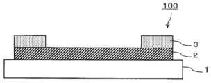
표시 장치를 더욱 협액연화하기 위해서는, 패턴 배선을 세선화하고, 또한 배선의 저항의 상승을 억제하기 위하여 도전성이 높은 배선 재료를 사용할 필요가 있다. 이러한 관점에서, 도 4 에 나타내는 바와 같이, 기재 (1) 상에 투명 도전성 박막 (25) 을 형성하고, 그 위에 구리로 이루어지는 금속층 (3) 을 형성한 적층체 (11) 를 제작하고, 금속층 (3), 투명 도전성 박막 (25) 을 순차 에칭에 의해 선택 제거하여 패턴화하는 방법이 제안되어 있다 (예를 들어 특허문헌 1).In order to further soften the display device, it is necessary to thin the pattern wiring and use a highly conductive wiring material in order to suppress an increase in resistance of the wiring. From this point of view, as shown in Fig. 4, a
한편, 상기와 같은 협액연화의 요구에 더하여, 투명 전극의 센서 감도나 분해능 향상의 관점에서, 저저항의 투명 도전성 박막을 사용하는 것이 요망되고 있다. 특히, 투영형 정전 용량 방식의 터치 패널에 있어서는, 투명 전극간의 미소한 정전 용량이 변화를 감지함으로써, 위치 검출을 실시하고 있고, 위치 검출 정밀도의 향상이나 응답 시간 단축을 위하여, 투명 도전성 박막의 저저항화가 요구되고 있다. 또, 저항 특성은 센서 감도 등을 결정함에 있어서의 사양이기 때문에, 양산시에는 투명 도전성 박막이 안정적인 저항 특성을 유지하는 것이 중요해진다.On the other hand, it is desired to use a transparent conductive thin film of low resistance from the viewpoint of improving the sensor sensitivity and resolution of the transparent electrode in addition to the above-mentioned requirement for the softening of the liquid. Particularly, in the touch panel of the projected capacitive type, the position detection is performed by detecting a change in the microcapacitance between the transparent electrodes. Resistance is required. Moreover, since the resistance characteristic is a specification for determining sensor sensitivity and the like, it is important for the transparent conductive thin film to maintain stable resistance characteristics during mass production.
상기의 특허문헌 1 과 같은 방법에 의하면, 에칭에 의해 패턴 배선을 형성할 수 있기 때문에, 패턴 배선의 세선화가 가능하고, 표시 장치의 협액연화가 가능해진다. 그러나, 본 발명자들의 검토에 의하면, 에칭에 의해 금속층을 제거한 후의 투명 도전성 박막은, 금속층을 형성하기 전의 투명 도전성 박막에 비하여 저항이 상승하는 경우가 있고, 특히, 저저항의 투명 도전성 박막에 있어서, 금속층을 에칭 제거 후의 저항 상승이 현저하였다.According to the same method as in
본 발명은 상기를 감안하여, 금속층을 에칭에 의해 제거하여 패턴 배선을 형성한 후에 있어서도 투명 도전성 박막의 저항의 상승이 억제되어, 패턴 배선이 형성된 투명 도전성 적층체의 형성에 적절한 도전성 적층체를 제공하는 것을 목적으로 한다.In view of the above, the present invention provides a conductive laminate suitable for forming a transparent conductive laminate in which pattern wiring is formed by suppressing an increase in resistance of the transparent conductive thin film even after removing the metal layer by etching to form a pattern wiring. It aims to do.
본 발명자들이 예의 검토한 결과, 투명 도전성 박막을 불순물 금속의 함유량이 상이한 2 층 이상의 투명 도전성 박막의 적층체로 함으로써, 저항의 상승이 억제되는 것을 알아내어 본 발명에 이르렀다.As a result of earnest examination by the present inventors, it has been found that the increase in resistance is suppressed by using a transparent conductive thin film as a laminate of two or more layers of transparent conductive thin films having different impurity metal contents, to reach the present invention.
본 발명은, 투명 기재의 적어도 일방의 면에, 적어도 2 층의 투명 도전성 박막으로 이루어지는 투명 도전성 박막 적층체 및 금속층이 이 순서로 형성된 도전성 적층체에 관한 것이다. 상기 투명 도전성 박막 적층체에 있어서, 금속층에 가장 근접한 제 1 투명 도전성 박막은, 금속 산화물층 또는 주 (主) 금속과 1 종 이상의 불순물 금속을 함유하는 복합 금속 산화물층이다. 투명 도전성 박막 적층체 중의 제 1 투명 도전성 박막 이외의 투명 도전성 박막은, 주금속과 1 종 이상의 불순물 금속을 함유하는 복합 금속 산화물층이다. 본 발명의 도전성 적층체에 있어서, 상기 제 1 투명 도전성 박막에 있어서의 불순물 금속의 함유비가, 상기 투명 도전성 박막 적층체를 구성하는 각 투명 도전성 박막에 있어서의 불순물 금속의 함유비 중에서 최대가 아니다.The present invention relates to a conductive laminate in which at least one surface of a transparent substrate is formed of a transparent conductive thin film laminate and a metal layer composed of at least two layers of transparent conductive thin films in this order. In the transparent conductive thin film laminate, the first transparent conductive thin film closest to the metal layer is a metal oxide layer or a composite metal oxide layer containing a main metal and one or more impurity metals. The transparent conductive thin film other than the first transparent conductive thin film in the transparent conductive thin film laminate is a composite metal oxide layer containing a main metal and at least one impurity metal. In the conductive laminate of the present invention, the content ratio of the impurity metal in the first transparent conductive thin film is not the largest among the content ratios of impurity metal in each transparent conductive thin film constituting the transparent conductive thin film laminate.
본 발명에 있어서는, 제 1 투명 도전성 박막에 있어서의 불순물 금속의 함유비가, 투명 도전성 박막 적층체를 구성하는 각 투명 도전성 박막에 있어서의 불순물 금속의 함유비 중에서 최소인 것이 바람직하다. 또, 투명 도전성 박막 적층체 중에서 가장 불순물 금속의 함유비가 큰 투명 도전성 박막에 있어서의 불순물 금속의 함유비와, 상기 제 1 투명 도전성 박막에 있어서의 불순물 금속의 함유비의 차가, 0.005 ∼ 0.23 인 것이 바람직하다.In the present invention, the content ratio of the impurity metal in the first transparent conductive thin film is preferably the minimum among the content ratio of the impurity metal in each transparent conductive thin film constituting the transparent conductive thin film laminate. Further, the difference between the content ratio of the impurity metal in the transparent conductive thin film and the content ratio of the impurity metal in the first transparent conductive thin film is 0.005 to 0.23. desirable.
본 발명에 있어서는, 제 1 투명 도전성 박막에 있어서의 불순물 금속의 함유비는 0.08 이하인 것이 바람직하다. 또, 투명 도전성 박막 적층체 중에서 가장 불순물 금속의 함유비가 높은 투명 도전성 박막에 있어서의 불순물 금속의 함유비가 0.04 ∼ 0.31 인 것이 바람직하다.In the present invention, the content ratio of the impurity metal in the first transparent conductive thin film is preferably 0.08 or less. Moreover, it is preferable that the content ratio of the impurity metal in the transparent conductive thin film which has the highest content ratio of impurity metal among the transparent conductive thin film laminates is 0.04 to 0.31.
제 1 투명 도전성 박막의 두께는, 투명 도전성 박막 적층체의 전체의 두께에 대해 6 % 이상인 것이 바람직하다. 또, 제 1 투명 도전성 박막의 두께는 투명 도전성 박막 적층체의 두께에 대해 50 % 미만인 것이 바람직하다.It is preferable that the thickness of the first transparent conductive thin film is 6% or more with respect to the total thickness of the transparent conductive thin film laminate. Moreover, it is preferable that the thickness of a 1st transparent conductive thin film is less than 50% with respect to the thickness of a transparent conductive thin film laminated body.
본 발명의 일 실시형태에 있어서, 상기 투명 도전성 박막 적층체를 구성하는 모든 투명 도전성 박막은 주금속이 In 이다. 이 경우, 불순물 금속으로서 Sn 을 함유하는 것이 바람직하다. 당해 실시형태에 있어서는, 제 1 투명 도전성 박막에 있어서의 In 에 대한 Sn 의 함유비가 0.08 이하인 것이 바람직하다. 또, 제 1 투명 도전성 박막 이외의 상기 투명 도전성 박막 적층체를 구성하는 투명 도전성 박막 전체에 있어서의 In 에 대한 Sn 의 함유비가, 0.08 ∼ 0.13 인 것이 바람직하다.In one embodiment of the present invention, all of the transparent conductive thin films constituting the transparent conductive thin film laminate have a main metal of In. In this case, it is preferable to contain Sn as an impurity metal. In this embodiment, it is preferable that the content ratio of Sn to In in the first transparent conductive thin film is 0.08 or less. Moreover, it is preferable that the content ratio of Sn with respect to In in the whole transparent conductive thin film which comprises the said transparent conductive thin film laminated body other than a 1st transparent conductive thin film is 0.08-0.13.
본 발명의 일 실시형태에 있어서, 투명 도전성 박막 적층체는, 제 1 투명 도전성 박막 및 제 1 투명 도전성 박막보다 기재측에 형성된 1 층의 투명 도전성 박막의 2 층으로 이루어진다. 본 발명의 일 실시형태에 있어서, 제 1 투명 도전성 박막과 금속층은 인접하고 있다. 본 발명의 일 실시형태에 있어서, 상기 투명 도전성 박막 적층체를 구성하는 모든 투명 도전성 박막이 결정질막이다. 본 발명의 일 실시형태에 있어서, 투명 기재가 가요성 필름이다.In one embodiment of the present invention, the transparent conductive thin film laminate comprises two layers of a first transparent conductive thin film and one transparent conductive thin film formed on the substrate side than the first transparent conductive thin film. In one embodiment of the present invention, the first transparent conductive thin film and the metal layer are adjacent. In one embodiment of the present invention, all the transparent conductive thin films constituting the transparent conductive thin film laminate are crystalline films. In one embodiment of the present invention, the transparent substrate is a flexible film.
또한, 본 발명은 상기 도전성 적층체를 사용하여 제조될 수 있는 패턴 배선이 형성된 투명 도전성 적층체에 관한 것이다. 당해 투명 도전성 적층체는, 투명 기재 상에, 패턴화된 복수의 투명 전극으로 이루어지는 투명 전극부 및 패턴 배선부를 갖고, 패턴 배선부가 각 투명 전극부에 접속되어 있다. 이와 같은 패턴 배선이 형성된 투명 도전성 적층체는, 상기 도전성 적층체의 금속층의 면내의 일부를 에칭에 의해 제거하여 패턴 배선부를 형성하고, 금속층이 제거된 투명 도전성 박막 적층체의 노출부에 있어서, 투명 도전성 박막 적층체의 면내의 일부를 에칭에 의해 제거하여 패턴화된 투명 전극을 형성함으로써 얻어진다.In addition, the present invention relates to a transparent conductive laminate in which pattern wiring that can be manufactured using the conductive laminate is formed. The transparent conductive laminate has a transparent electrode portion and a pattern wiring portion formed of a plurality of patterned transparent electrodes on a transparent substrate, and the pattern wiring portion is connected to each transparent electrode portion. The transparent conductive laminate having such pattern wiring is formed by removing a part of the surface of the metal layer of the conductive laminate by etching to form a pattern wiring portion, and in the exposed portion of the transparent conductive thin film laminate with the metal layer removed, the transparent It is obtained by removing a part of the surface of the conductive thin film laminate by etching to form a patterned transparent electrode.
본 발명의 도전성 적층체는, 투명 도전층으로서 적어도 2 층의 투명 도전성 박막으로 이루어지는 투명 도전성 박막 적층체를 갖고, 금속층에 가장 근접한 제 1 투명 도전성 박막의 불순물 금속 함유비가 상대적으로 작다. 그 때문에, 투명 도전성 박막 적층체 상에 형성된 금속층의 면내의 일부를 에칭에 의해 제거하여 패턴화를 실시한 경우에도, 투명 도전성 박막 적층체의 저항의 상승이 억제된다. 본 발명의 도전 적층체를 에칭에 의해 패턴화하여 얻어지는 패턴 배선이 형성된 투명 도전성 적층체는, 투명 도전성 박막이 저저항이며, 또한 안정적인 저항 특성을 유지할 수 있다.The conductive laminate of the present invention has a transparent conductive thin film laminate composed of at least two transparent conductive thin films as a transparent conductive layer, and the content of impurity metal in the first transparent conductive thin film closest to the metal layer is relatively small. Therefore, even when patterning is performed by removing a part of the metal layer formed on the transparent conductive thin film laminate by etching, the increase in resistance of the transparent conductive thin film laminate is suppressed. In the transparent conductive laminate in which the pattern wiring obtained by patterning the conductive laminate of the present invention by etching is formed, the transparent conductive thin film has low resistance and can maintain stable resistance characteristics.
도 1 은 본 발명의 일 실시형태에 관련된 도전성 적층체의 모식적 단면도이다.
도 2 는 본 발명의 일 실시형태에 관련된 도전성 적층체의 모식적 단면도이다.
도 3 은 본 발명의 일 실시형태에 관련된 도전성 적층체의 모식적 단면도이다.
도 4 는 종래 기술에 있어서의 도전성 적층체의 일 형태를 나타내는 모식적 단면도이다.
도 5 는 본 발명의 실시의 일 형태에 관련된 패턴 배선이 형성된 투명 도전성 적층체의 모식적 평면도이다.
도 6 은 도 5 의 Ⅵ-Ⅵ 선에 있어서의 단면을 모식적으로 나타내는 도면이다.
도 7 은 패턴 배선이 형성된 투명 도전성 적층체의 제조 과정을 설명하기 위한 모식적 평면도이다.1 is a schematic cross-sectional view of a conductive laminate according to an embodiment of the present invention.
2 is a schematic cross-sectional view of a conductive laminate according to an embodiment of the present invention.
3 is a schematic cross-sectional view of a conductive laminate according to an embodiment of the present invention.
4 is a schematic cross-sectional view showing one embodiment of a conductive laminate in the prior art.
5 is a schematic plan view of a transparent conductive laminate in which pattern wiring according to an embodiment of the present invention is formed.
It is a figure which shows typically the cross section in line VI-VI of FIG.
7 is a schematic plan view for explaining a manufacturing process of a transparent conductive laminate in which pattern wiring is formed.
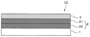
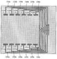
본 발명의 실시형태에 대해, 도면을 참조하면서 이하에 설명한다. 도 1 은, 본 발명의 도전성 적층체의 일 실시형태를 나타내는 모식적 단면도이고, 도 5 는, 본 발명의 패턴 배선이 형성된 투명 도전성 적층체의 모식적 평면도이고, 도 6 은, 도 5 의 Ⅵ-Ⅵ 선에 있어서의 단면을 모식적으로 나타내는 단면도이다. 본 발명의 도전성 적층체 (10) 는, 투명 기재 (1) 의 적어도 일방의 면에 투명 도전성 박막 적층체 (2) 및 금속층 (3) 이 순차 형성되어 있다. 투명 도전성 박막 적층체 (2) 는, 적어도 2 층의 투명 도전성 박막 (21, 22) 으로 이루어진다.Embodiments of the present invention will be described below with reference to the drawings. 1 is a schematic cross-sectional view showing one embodiment of the conductive laminate of the present invention, FIG. 5 is a schematic plan view of the transparent conductive laminate in which the pattern wiring of the present invention is formed, and FIG. 6 is VI of FIG. 5 It is a cross-sectional view schematically showing a section in line VI. In the
<도전성 적층체> <Conductive laminate>
(투명 기재)(Transparent description)
투명 기재 (1) 로는, 가시광 영역에 있어서 투명한 것이면 특별히 제한되지 않고, 유리나, 투명성을 갖는 각종의 플라스틱 필름이 사용된다. 후술하는 패턴 배선이 형성된 투명 도전성 적층체를, 터치 패널의 투명 전극이나 플렉시블 디스플레이 등에 사용하는 경우에는, 투명 기재로서 플라스틱 필름 등의 가요성 필름이 사용되는 것이 바람직하다. 플라스틱 필름의 재료로는, 폴리에스테르계 수지, 아세테이트계 수지, 폴리에테르술폰계 수지, 폴리카보네이트계 수지, 폴리아미드계 수지, 폴리이미드계 수지, 폴리올레핀계 수지, (메트)아크릴계 수지, 폴리염화비닐계 수지, 폴리염화비닐리덴계 수지, 폴리스티렌계 수지, 폴리비닐알코올계 수지, 폴리아릴레이트계 수지, 폴리페닐렌술파이드계 수지 등을 들 수 있다. 이들 중에서 특히 바람직한 것은, 폴리에스테르계 수지, 폴리카보네이트계 수지, 폴리올레핀계 수지 등을 들 수 있다.The
투명 기재로서 플라스틱 필름이 사용되는 경우, 그 두께는 2 ∼ 200 ㎛ 의 범위 내인 것이 바람직하고, 2 ∼ 100 ㎛ 의 범위 내인 것이 보다 바람직하다. 필름의 두께가 2 ㎛ 미만이면, 투명 기재의 기계적 강도가 부족하고, 필름을 롤상으로 하여 투명 도전성 박막 적층체 (2) 나 금속층 (3) 을 연속적으로 형성하는 조작이 곤란해지는 경우가 있다. 한편, 필름의 두께가 200 ㎛ 를 초과하면, 디바이스의 두께가 커지는 것에 더하여, 투명 도전성 박막이 내찰상성이 떨어지는 경향이 있다.When a plastic film is used as the transparent substrate, the thickness is preferably in the range of 2 to 200 μm, and more preferably in the range of 2 to 100 μm. When the thickness of the film is less than 2 µm, the mechanical strength of the transparent substrate is insufficient, and the operation of continuously forming the transparent conductive
투명 기재에는, 표면에 미리 스퍼터링, 코로나 방전, 화염, 자외선 조사, 전자선 조사, 화성, 산화 등의 에칭 처리나 하도 처리를 실시하고, 필름 기재 상에 형성되는 투명 도전성 박막과의 밀착성을 향상시키도록 해도 된다. 또, 투명 도전성 박막을 형성하기 전에, 필요에 따라 용제 세정이나 초음파 세정 등에 의해, 기재 표면을 제진, 청정화해도 된다.To the transparent substrate, the surface is subjected to etching treatment or primer treatment such as sputtering, corona discharge, flame, ultraviolet irradiation, electron beam irradiation, chemical conversion, oxidation, etc. in advance to improve adhesion to the transparent conductive thin film formed on the film substrate. You may do it. Moreover, before forming a transparent conductive thin film, if necessary, the surface of a base material may be dusted and cleaned by solvent cleaning, ultrasonic cleaning, or the like.
또, 투명 기재 (1) 의 투명 도전성 박막 적층체 (2) 형성면에는, 유전체층이나 하드 코트층이 형성되어 있어도 된다. 투명 기재의 투명 도전성 박막 적층체 형성면측의 표면에 형성되는 유전체층은, 도전층으로서의 기능을 갖지 않는 것으로, 표면 저항이, 예를 들어 1×10⁶ Ω/□ 이상이고, 바람직하게는 1×10⁷ Ω/□ 이상, 더욱 바람직하게는 1×10⁸ Ω/□ 이상이다. 또한, 유전체층의 표면 저항의 상한은 특별히 없다. 일반적으로는, 유전체층의 표면 저항의 상한은 측정 한계인 1×10¹³ Ω/□ 정도인데, 1×10¹³ Ω/□ 를 초과하는 것이어도 된다.Moreover, a dielectric layer or a hard coat layer may be formed on the transparent conductive
유전체층의 재료로는, NaF (1.3), Na3AlF6 (1.35), LiF (1.36), MgF2 (1.38), CaF2 (1.4), BaF2 (1.3), SiO2 (1.46), LaF3 (1.55), CeF (1.63), Al2O3 (1.63) 등의 무기물 [( ) 내의 수치는 굴절률을 나타낸다] 이나, 굴절률이 1.4 ∼ 1.6 정도인 아크릴 수지, 우레탄 수지, 멜라민 수지, 알키드 수지, 실록산계 폴리머, 유기 실란 축합물 등의 유기물, 또는 상기 무기물과 상기 유기물의 혼합물을 들 수 있다.As the material of the dielectric layer, NaF (1.3), Na 3 AlF 6 (1.35), LiF (1.36), MgF 2 (1.38), CaF 2 (1.4), BaF 2 (1.3), SiO 2 (1.46), LaF 3 (1.55), inorganic materials such as CeF (1.63), Al 2 O 3 (1.63) [the values in () indicate the refractive index], but acrylic resins, urethane resins, melamine resins, alkyd resins having a refractive index of about 1.4 to 1.6, And organic materials such as siloxane-based polymers and organic silane condensates, or mixtures of the inorganic materials and the organic materials.
이와 같이, 투명 기재의 투명 도전성 박막 형성면측에 유전체층을 형성함으로써, 투명 도전성 박막 적층체 (2) 가 복수 영역에 패턴화된 경우에 있어서도, 투명 도전성 박막 형성 영역과 투명 도전성 박막 비형성 영역 사이의 시인성의 차를 저감시키는 것이 가능하다. 또, 투명 기재로서 필름 기재를 사용하는 경우에 있어서는, 유전체층이 플라스틱 필름으로부터의 올리고머 등의 저분자량 성분의 석출을 억제하는 봉지층으로서도 작용할 수 있다.Thus, by forming a dielectric layer on the transparent conductive thin film forming surface side of the transparent substrate, even when the transparent conductive
투명 기재 (1) 의 투명 도전성 박막 적층체 (2) 형성면과 반대측의 면에는, 필요에 따라 하드 코트층 등이 형성되어 있어도 된다. 또, 점착제 등의 적절한 접착 수단을 사용하여 다른 기재가 첩합 (貼合) 된 것이나, 다른 기재와 첩합시키기 위한 점착제층 등에 세퍼레이터 등의 보호층이 가착 (假着) 된 것이어도 된다. 또한, 도 1 ∼ 3 에 있어서는, 투명 기재 (1) 의 일방면에만 투명 도전성 박막 적층체 (2) 및 금속층 (3) 이 형성된 형태가 도시되어 있는데, 투명 기재의 양면에 투명 도전성 박막 적층체 및 금속층이 형성되어 있어도 된다.A hard coat layer or the like may be formed on the surface opposite to the surface of the
(투명 도전성 박막 적층체)(Transparent conductive thin film laminate)
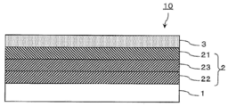
투명 기재 (1) 상에는, 투명 도전성 박막 적층체 (2) 가 형성된다. 투명 도전성 박막 적층체는, 적어도 2 층의 투명 도전성 박막 (21, 22) 이 적층된 것이다. 투명 도전성 박막 적층체 (2) 는, 도 2 에 나타내는 바와 같이 3 층의 투명 도전성 박막 (21, 22, 23) 을 갖고 있어도 되고, 4 층 이상의 투명 도전성 박막을 갖고 있어도 된다.On the
이들의 투명 도전성 박막은 모두, 금속의 도전성 산화물을 주성분으로 하는 박막, 또는 주금속과 1 종 이상의 불순물 금속을 함유하는 복합 금속 산화물을 주성분으로 하는 박막이다. 이들의 도전성 박막은, 투명하고 또한 도전성을 갖는 것이면, 그 구성 재료는 특별히 한정되지 않고, Sc, Y, Ti, Zr, Hf, V, Nb, Ta, Cr, Mo, W, Mn, Tc, Re, Fe, Ru, Os, Co, Rh, Ir, Ni, Pd, Pt, Cu, Ag, Au, Zn, Cd, Al, Ga, Ti, Ge, In, Sn, Pb, As, Sb, Bi, Se, Te, I 로 이루어지는 군에서 선택되는 1 종의 금속을 주성분으로 하는 금속 산화물이 바람직하게 사용된다. 투명 도전성 박막의 투명성이나 도전성의 관점에서는, 주금속 원소는 In, Zn, Sn 중 어느 것인 것이 바람직하고, In 이 가장 바람직하다. 투명 도전성 박막이, 주금속과 불순물 금속을 함유하는 복합 금속 산화물인 경우, 불순물 금속으로서도, 상기 군에서 선택되는 1 종 이상의 금속이 바람직하게 사용된다.All of these transparent conductive thin films are thin films mainly composed of a conductive oxide of a metal, or thin films mainly composed of a composite metal oxide containing a main metal and one or more impurity metals. These conductive thin films are not particularly limited as long as they are transparent and have conductivity. Sc, Y, Ti, Zr, Hf, V, Nb, Ta, Cr, Mo, W, Mn, Tc, Re , Fe, Ru, Os, Co, Rh, Ir, Ni, Pd, Pt, Cu, Ag, Au, Zn, Cd, Al, Ga, Ti, Ge, In, Sn, Pb, As, Sb, Bi, Se , Te, I, a metal oxide containing one kind of metal selected from the group as a main component is preferably used. From the viewpoint of transparency and conductivity of the transparent conductive thin film, the main metal element is preferably any of In, Zn, and Sn, and In is most preferred. When the transparent conductive thin film is a composite metal oxide containing a main metal and an impurity metal, one or more metals selected from the above group are preferably used as the impurity metal.
투명 도전성 박막의 캐리어 밀도를 상승시켜 투명 도전성 박막을 저저항화하는 관점에 있어서는, 복합 금속 산화물에 있어서의 불순물 금속은, 주금속보다 가전자 (假電子) 수가 많은 것이 바람직하게 사용된다. 이와 같은 복합 금속 산화물로는, 주석 도프 산화인듐 (ITO), 안티몬 도프 산화주석 (ATO), 알루미늄 도프 산화아연 (AZO), 갈륨 도프 산화아연 (GZO), 인듐 도프 산화아연 (IZO) 등을 들 수 있다. 그 중에서도 저저항 또한 고투명의 투명 도전성 박막을 형성하는 관점 에 있어서, ITO 가 가장 바람직하게 사용된다.From the viewpoint of increasing the carrier density of the transparent conductive thin film to lower the resistance of the transparent conductive thin film, it is preferable that the impurity metal in the composite metal oxide has more valence than the main metal. Examples of such composite metal oxides include tin-doped indium oxide (ITO), antimony-doped tin oxide (ATO), aluminum-doped zinc oxide (AZO), gallium-doped zinc oxide (GZO), and indium-doped zinc oxide (IZO). Can. Among them, ITO is most preferably used from the viewpoint of forming a low-resistance and highly transparent transparent conductive thin film.
본 발명에 있어서는, 투명 도전성 박막 적층체 (2) 상에 형성되는 금속층 (3) 에 가장 근접한 제 1 투명 도전성 박막 (21) 에 있어서의 불순물 금속의 함유비가, 투명 도전성 박막 적층체를 구성하는 각 투명 도전성 박막 (22, 23) 에 있어서의 불순물 금속의 함유비 중에서 최대가 아닌 것을 특징으로 한다. 예를 들어, 도 1 에 나타내는 바와 같이, 투명 도전성 박막 적층체 (2) 가 2 층의 투명 도전성 박막 (21, 22) 으로 이루어지는 경우, 금속층 (3) 에 가까운 측의 제 1 투명 도전성 박막 (21) 에 있어서의 불순물 금속의 함유비는, 투명 기재 (1) 측의 투명 도전성 박막 (22) 에 있어서의 불순물 금속의 함유비보다 작다.In the present invention, the content ratio of the impurity metal in the first transparent conductive
이와 같이, 금속층 (3) 에 가장 근접한 제 1 투명 도전성 박막 (21) 의 불순물 금속 함유비를 작게 함으로써, 투명 도전성 박막 적층체 (2) 상에 금속층 (3) 을 형성하고, 그 면내의 일부를 에칭에 의해 제거하여 패턴화를 실시했을 때의 투명 도전성 박막 적층체의 저항의 변화가 억제된다.In this way, by reducing the content of the impurity metal in the first transparent conductive
본 발명자들의 검토에 의하면, 투명 도전성 박막의 불순물 금속의 함유비가 많은 경우에는, 투명 도전성 박막 상에 형성된 금속층을 에칭에 의해 제거했을 때에 캐리어 밀도가 저하되어, 저항이 증대하기 쉬운 것이 판명되었다. 즉, 도 4 에 나타내는 바와 같이, 1 층의 투명 도전성 박막 (25) 상에 금속층 (3) 을 적층한 형태에 있어서는, 투명 도전성 박막 (25) 을 저저항막으로 하기 위해서, 불순물 금속 함유비가 큰 복합 금속 산화물을 사용하면, 금속층 (3) 을 에칭에 의해 제거한 후의 도전성막 (25) 의 저항이 증대되는 경향이 있다.According to the studies of the present inventors, when the content ratio of the impurity metal in the transparent conductive thin film was large, it was found that when the metal layer formed on the transparent conductive thin film was removed by etching, the carrier density was lowered and resistance was likely to increase. That is, as shown in FIG. 4, in the form in which the
이에 반하여, 본 발명에 있어서는, 기재 (1) 측에 불순물 금속의 함유비가 상대적으로 큰 복합 산화물 박막 (22) 을 갖고, 금속층 (3) 측에 불순물 금속의 함유비가 상대적으로 작은 복합 산화물 박막 (21) 을 사용함으로써, 투명 도전성 박막 적층체 전체로서의 비저항이 낮고, 또한 금속층 (3) 을 에칭에 의해 제거했을 때의 저항의 증대가 억제된다. 또한, 불순물 금속의 함유율이란, 투명 도전성 박막 중의 주금속 원소의 원자수 NP 에 대한 불순물 금속 원소의 원자수 ND 의 비 ND/NP 로 나타내진다.On the other hand, in the present invention, the composite oxide
제 1 투명 도전성 박막 (21) 의 불순물 금속 함유비를 작게 함으로써 금속층을 에칭 제거했을 때의 저항 증대가 억제되는 원인은 확실하지 않다. 추정 원인 중 하나로서, 불순물 금속 함유비가 큰 경우에는, 금속층 제거에 사용되는 에천트 중의 화학종과 불순물 금속의 착 형성 등에 의해 투명 도전성 박막의 캐리어 밀도가 저하되는 경향이 있고, 불순물 금속의 함유비를 작게 함으로써 이와 같은 에천트의 영향에 의한 저항 증대가 억제되는 것을 생각할 수 있다.It is unclear why the increase in resistance when the metal layer is etched and removed by reducing the content ratio of the impurity metal in the first transparent conductive
도 1 에 나타내는 바와 같이, 투명 도전성 박막 적층체 (2) 가 2 층의 투명 도전성 박막 (21, 22) 으로 이루어지는 경우, 투명 기재 (1) 측의 투명 도전성 박막 (22) 에 있어서의 불순물 금속의 함유비와 금속층 (3) 에 가까운 측의 제 1 투명 도전성 박막 (21) 에 있어서의 불순물 금속의 함유비의 차는, 0.005 ∼ 0.23 인 것이 바람직하고, 0.01 ∼ 0.23 인 것이 보다 바람직하고, 0.02 ∼ 0.23 인 것이 더욱 바람직하다. 또한, 상기의 불순물 금속의 함유비의 범위를, 투명 도전성 박막을 구성하는 복합 금속 산화물 박막으로서 인듐-주석 복합 산화물 (ITO) 이 사용되는 경우, 즉, 주금속이 인듐이고 불순물 금속이 주석인 경우에 있어서의, 투명 기재측의 투명 도전성 박막과 금속층측의 제 1 투명 도전성 박막 (21) 의 Sn 원자 함유량 (In2O3 과 SnO2 의 중량의 합계에 대한 SnO2 의 중량) 의 차로 나타내면, 대략 0.5 % ∼ 20 %, 1 % ∼ 20 %, 2 % ∼ 20 % 가 된다.As shown in Fig. 1, when the transparent conductive
또, 도 2 에 나타내는 바와 같이, 투명 도전성 박막 적층체 (2) 가 3 층 이상의 투명 도전성 박막으로 이루어지는 경우, 투명 도전성 박막 적층체 (2) 중에서 가장 불순물 금속의 함유비가 높은 투명 도전성 박막에 있어서의 불순물 금속의 함유비와 금속층 (3) 에 가까운 측의 제 1 투명 도전성 박막 (21) 에 있어서의 불순물 금속의 함유비의 차가, 0.005 ∼ 0.23 인 것이 바람직하고, 0.01 ∼ 0.23 인 것이 보다 바람직하고, 0.02 ∼ 0.23 인 것이 더욱 바람직하다. 투명 도전성 박막 적층체를 저저항막으로 하면서, 금속층을 에칭했을 때의 저항의 증대를 억제하는 관점에 있어서는, 투명 도전성 박막 적층체 (2) 중의 금속층 (3) 에 가까운 측의 제 1 투명 도전성 박막 (21) 이외의 투명 도전성 박막 (22, 23) 을 1 개의 막으로 간주한 경우의 불순물 금속의 함유비와 제 1 투명 도전성 박막 (21) 에 있어서의 불순물 금속의 함유비의 차가 상기 범위인 것이 바람직하다.Moreover, as shown in FIG. 2, when the transparent conductive thin film laminated
제 1 투명 도전성 박막에 있어서의 불순물 금속의 함유비와 그 밖의 투명 도전성 박막에 있어서의 불순물 금속의 함유비의 차가 과도하게 작으면, 투명 도전성 박막 적층체 (2) 내에서의 각 박막의 물리적인 상이가 작기 때문에, 도 4 에 나타내는 바와 같이 1 층만의 투명 도전성 박막만을 갖는 경우와 물성이 유사하다. 한편, 불순물 금속의 함유량의 차이가 과도하게 크면, 불순물 금속 함유량이 큰 투명 도전성 박막의 결정화가 저해되는 등의 이유에 의해 생산성이 떨어지거나 투명 도전성 박막 적층체를 저저항으로 하는 것이 곤란해지는 경우가 있다.If the difference between the content ratio of the impurity metal in the first transparent conductive thin film and the content ratio of the impurity metal in the other transparent conductive thin film is excessively small, the physical properties of each thin film in the transparent conductive
금속층 (3) 에 가장 근접한 제 1 투명 도전성 박막 (21) 에 있어서의 불순물 금속의 함유비는, 0.08 이하인 것이 바람직하고, 0.08 미만인 것이 바람직하고, 0.05 이하인 것이 보다 바람직하다. 제 1 투명 도전성 박막의 불순물 금속 함유비가 커지면, 금속층 (3) 을 에칭했을 때에, 도전성 박막 적층체의 표면 저항이 증대되는 경향이 있다. 또한, 상기의 불순물 금속의 함유비의 범위를, 투명 도전성 박막을 구성하는 복합 금속 산화물 박막으로서 인듐-주석 복합 산화물 (ITO) 이 사용되는 경우에 있어서의, 투명 기재측의 투명 도전성 박막과 금속층측의 제 1 투명 도전성 박막 (21) 의 Sn 원자 함유량 (In2O3 과 SnO2 의 중량의 합계에 대한 SnO2 의 중량) 으로 나타내면, 대략 8 %, 5 % 가 된다. 제 1 투명 도전성 박막 (21) 에 있어서의 불순물 금속의 함유비의 최소치는 0 이다. 즉, 제 1 투명 도전성 박막 (21) 은, 예를 들어 산화인듐과 같은 단일의 금속의 산화물막이어도 된다.The content ratio of the impurity metal in the first transparent conductive
투명 도전성 박막 적층체 (2) 중에서 가장 불순물 금속의 함유비가 높은 투명 도전성 박막에 있어서의 불순물 금속의 함유비는, 0.04 ∼ 0.31 인 것이 바람직하고, 0.04 ∼ 0.24 인 것이 보다 바람직하다. 도 1 에 나타내는 바와 같이 투명 도전성 박막 적층체 (2) 가 2 층의 투명 도전성 박막으로 이루어지는 경우에는, 투명 기재 (1) 측의 투명 도전성 박막 (22) 에 있어서의 불순물 금속의 함유비가 상기 범위인 것이 바람직하다. 도 2 에 나타내는 바와 같이 투명 도전성 박막 적층체 (2) 가 3 층 이상의 투명 도전성 박막으로 이루어지는 경우, 투명 도전성 박막 적층체 (2) 중에서 가장 불순물 금속의 함유비가 높은 투명 도전성 박막에 있어서의 불순물 금속의 함유비가 상기 범위이면 된다. 투명 도전성 박막 적층체 (2) 의 비저항을 작게 하는 관점에 있어서는, 투명 도전성 박막 적층체 (2) 중의 금속층 (3) 에 가까운 측의 제 1 투명 도전성 박막 (21) 이외의 투명 도전성 박막을 1 개의 막으로 간주한 경우의 불순물 금속의 함유비가 상기 범위인 것이 특히 바람직하다. 또한, 상기의 불순물 금속의 함유비의 범위를, 투명 도전성 박막을 구성하는 복합 금속 산화물 박막으로서 인듐-주석 복합 산화물 (ITO) 이 사용되는 경우에 있어서의, 투명 기재측의 투명 도전성 박막과 금속층측의 제 1 투명 도전성 박막 (21) 의 Sn 원자 함유량 (In2O3 과 SnO2 의 중량의 합계에 대한 SnO2 의 중량) 으로 나타내면, 대략 4 % ∼ 25 %, 4 % ∼ 21 % 가 된다.The content ratio of the impurity metal in the transparent conductive thin film having the highest impurity metal content among the transparent conductive
제 1 투명 도전성 박막 (21) 의 두께는, 1 ㎚ 이상인 것이 바람직하다. 또, 제 1 투명 도전성 박막 (21) 의 두께는, 1 ㎚ ∼ 17 ㎚ 인 것이 바람직하고, 1 ㎚ ∼ 12 ㎚ 인 것이 보다 바람직하고, 1 ㎚ ∼ 6 ㎚ 인 것이 더욱 바람직하다. 투명 도전성 박막 적층체 (2) 중의 제 1 투명 도전성 박막 (21) 이외의 투명 도전성 박막의 두께의 합계는, 9 ㎚ ∼ 34 ㎚ 인 것이 바람직하고, 9 ∼ 29 ㎚ 인 것이 보다 바람직하고, 9 ∼ 24 ㎚ 인 것이 더욱 바람직하다. 각 층의 두께는, 상기 범위를 채용할 수 있는데, 투명 도전성 박막 적층체의 비저항을 작게 하는 관점에서는, 제 1 투명 도전성 박막 (21) 의 두께가, 제 1 투명 도전성 박막 (21) 이외의 투명 도전성 박막의 두께의 합계보다 작아지도록, 각 투명 도전성 박막을 형성하는 것이 바람직하다. 제 1 투명 도전성 박막 (21) 의 두께와 제 1 투명 도전성 박막 (21) 이외의 투명 도전성 박막의 두께의 합계의 차는, 1 ㎚ 이상인 것이 바람직하고, 나아가서는 1 ㎚ ∼ 33 ㎚ 인 것이 보다 바람직하고, 1 ㎚ ∼ 20 ㎚ 인 것이 더욱 바람직하다.It is preferable that the thickness of the first transparent conductive
적층체를 고투과율로 하는 관점에서는, 투명 도전성 박막 적층체 전체의 두께는, 35 ㎚ 이하인 것이 바람직하고, 30 ㎚ 이하인 것이 바람직하다. 또, 투명 도전성 박막 적층체 (2) 의 전체의 두께에 대한 제 1 투명 도전성 박막 (21) 의 두께의 비율은, 6 % 이상인 것이 바람직하고, 6 % ∼ 45 % 인 것이 보다 바람직하고, 6 % ∼ 35 % 인 것이 더욱 바람직하다. 두께 비율을 상기 범위로 함으로써, 투명 도전성 박막 적층체가 저저항 특성을 유지하면서, 결정화 속도를 높일 수 있기 때문에, 저항 안정성이 우수한 투명 도전막을 높은 생산 효율로 얻을 수 있다.From the viewpoint of making the laminate high transmittance, the thickness of the entire transparent conductive thin film laminate is preferably 35 nm or less, and preferably 30 nm or less. Moreover, the ratio of the thickness of the first transparent conductive
투명 도전성 박막 적층체를 구성하는 각 투명 도전성 박막의 형성 방법은 특별히 한정되지 않고, 종래 공지된 방법을 채용할 수 있다. 구체적으로는, 예를 들어 진공 증착법, 스퍼터링법, 이온 플레이팅법을 예시할 수 있다. 또, 필요로 하는 막두께에 따라 적절한 방법을 채용할 수도 있다.The method for forming each transparent conductive thin film constituting the transparent conductive thin film laminate is not particularly limited, and a conventionally known method can be adopted. Specifically, a vacuum evaporation method, sputtering method, and ion plating method can be illustrated, for example. Moreover, an appropriate method can also be employed depending on the required film thickness.
각 투명 도전성 박막은 결정질이어도 되고, 비정질이어도 된다. 예를 들어, 투명 기재로서 플라스틱 필름이 사용되고, 투명 도전성 박막으로서 스퍼터링법 에 의해 ITO 막이 형성되는 경우, 기재의 내열성에 의한 제약이 있기 때문에, 높은 온도에서 스퍼터 제막을 실시할 수 없다. 그 때문에, 제막 직후의 투명 도전성 박막은 비정질막 (일부가 결정화되어 있는 경우도 있다) 으로 되어 있는 경우가 많다. 이와 같은 비정질의 투명 도전성 박막은 결정질인 것에 비하여 투과율이 낮고, 가습열 시험 후의 저항 변화가 큰 등의 문제를 일으키는 경우가 있다. 이러한 관점에서는, 일단 비정질의 투명 도전성 박막을 형성한 후, 대기 중의 산소 존재 하에서 가열함으로써, 결정막으로 전환시켜도 된다. 투명 도전성 박막을 결정화함으로써, 투명성이 향상되고, 저저항화가 도모됨과 함께, 또한 가습열 시험 후의 저항 변화가 작아, 가습열 신뢰성이 향상되는 등의 이점을 가져온다.Each transparent conductive thin film may be crystalline or amorphous. For example, when a plastic film is used as a transparent substrate and an ITO film is formed by a sputtering method as a transparent conductive thin film, sputter film formation cannot be performed at a high temperature because there is a limitation due to heat resistance of the substrate. For this reason, the transparent conductive thin film immediately after film formation is often an amorphous film (some may be crystallized). Such an amorphous transparent conductive thin film may cause problems such as a low transmittance and a large change in resistance after a humidification heat test compared to that of a crystalline one. From this viewpoint, the amorphous transparent conductive thin film may be formed once, and then heated in the presence of oxygen in the atmosphere to convert to a crystalline film. By crystallizing the transparent conductive thin film, the transparency is improved, the resistance is lowered, the resistance change after the humidification heat test is small, and the advantages such as improved humidification heat reliability are brought.
각 투명 도전성 박막의 결정화는, 투명 기재 (1) 상에 비정질의 막을 형성 후, 금속층 (3) 을 제막하기 전에 실시할 수도 있고, 금속층을 제막한 후에 결정화를 실시해도 된다. 또, 에칭 등에 의해 투명 도전성 박막 적층체를 패턴화하는 경우, 투명 도전성 박막의 결정화는, 에칭 가공 전에 실시할 수도 있고, 에칭 가공 후에 실시해도 된다.Crystallization of each transparent conductive thin film may be performed after forming an amorphous film on the
(금속층)(Metal layer)
투명 도전성 박막 적층체 (2) 상에는, 금속층 (3) 이 형성된다. 또한, 제 1 투명 도전성 박막 (21) 과 금속층 (3) 사이에는, 투명 도전성 박막 적층체와 금속층의 밀착성 향상이나, 금속층을 구성하는 금속 원소의 투명 도전층으로의 확산 방지 등의 관점에서, 예를 들어 두께가 5 ㎚ 이하인 박막을 형성할 수도 있다. 한편, 금속층 (3) 을 에칭에 의해 제거했을 때의 투명 도전성 박막 적층체의 표면 저항의 증가를 억제하는 관점에 있어서는, 제 1 투명 도전성 박막 (21) 상에 직접 금속층 (3) 이 형성되는 것이 바람직하다.On the transparent conductive
금속층의 구성 재료는, 도전성을 갖는 것이면 특별히 한정되지 않고, 예를 들어, Ti, Si, Nb, In, Zn, Sn, Au, Ag, Cu, Al, Co, Cr, Ni, Pb, Pd, Pt, W, Zr, Ta, Hf 등의 금속이 바람직하게 사용된다. 또, 이들 금속의 2 종 이상을 함유하는 것이나, 이들 금속을 주성분으로 하는 합금 등도 바람직하게 사용할 수 있다. 도전성 적층체를 형성한 후에 금속층 (3) 의 면내의 일부를 에칭 등에 의해 제거하여, 도 5 에 나타내는 바와 같은 패턴 배선을 형성하는 경우에는, 금속층 (3) 의 재료로서 Au, Ag, Cu 등의 도전성이 높은 금속이 바람직하게 사용된다. 그 중에서도 Cu 는 도전성이 높으며, 또한 저렴한 재료이기 때문에, 배선을 구성하는 재료로서 적합하다. 그 때문에, 금속층 (3) 은 실질적으로 구리로 이루어지는 것이 특히 바람직하다.The material of the metal layer is not particularly limited as long as it has conductivity. For example, Ti, Si, Nb, In, Zn, Sn, Au, Ag, Cu, Al, Co, Cr, Ni, Pb, Pd, Pt , W, Zr, Ta, Hf and the like are preferably used. Moreover, what contains 2 or more types of these metals, the alloy etc. which have these metals as a main component can also be used preferably. After forming a conductive laminate, part of the surface of the
금속층 (3) 의 두께는 특별히 제한되지 않는다. 예를 들어, 도전성 필름의 형성 후에 금속층 (3) 의 면내의 일부를 에칭 등에 의해 제거하여 패턴 배선을 형성하는 경우에는, 형성 후의 패턴 배선이 원하는 저항값을 갖도록 금속층 (3) 의 두께가 적절히 설정된다. 금속층의 두께가 과도하게 작으면, 패턴 배선의 저항이 지나치게 높아지기 때문에, 디바이스의 소비 전력이 커지는 경우가 있다. 그 때문에, 금속층의 두께는 20 ㎚ 이상인 것이 바람직하다. 반대로 금속층의 두께가 과도하게 크면, 금속층의 성막에 시간을 필요로 하기 때문에 생산성이 떨어지는 것 외에, 성막시의 적산 열량이 커지는 경우나, 성막시의 파워 밀도를 높게 할 필요가 있기 때문에, 필름에 열 주름이 발생하기 쉬워지는 경향이 있다. 이들의 관점에서, 금속층의 두께는 20 ㎚ ∼ 500 ㎚ 인 것이 바람직하다.The thickness of the
금속층은, 막두께의 균일성이나 성막 효율의 관점에서, 화학 기상 성장법 (CVD) 이나 물리 기상 성장법 (PVD) 등의 진공 성막법이나, 도금법 (전해 도금, 무전해 도금) 등에 의해 성막되는 것이 바람직하다. 또, 이들 제막 방법의 복수를 조합하여도 된다. 그 중에서도, 진공 증착법, 스퍼터링법, 이온 플레이팅법, 전자빔 증착법 등의 물리 기상 성장법이 바람직하고, 스퍼터링법이 특히 바람직하다.The metal layer is formed by vacuum deposition methods such as chemical vapor deposition (CVD) or physical vapor deposition (PVD), plating methods (electrolytic plating, electroless plating), etc. from the viewpoint of uniformity of film thickness and deposition efficiency. It is preferred. Moreover, you may combine multiple of these film forming methods. Among them, physical vapor deposition methods such as vacuum deposition, sputtering, ion plating, and electron beam deposition are preferred, and sputtering is particularly preferred.
도 3 에 나타내는 바와 같이, 금속층 (3) 상에, 추가로 산화 방지를 목적으로 한 제 2 금속층 (4) 을 형성해도 된다. 예를 들어, 금속층 (3) 상에 금속층 (3) 과는 상이한 조성을 갖는 제 2 금속층 (4) 을 가짐으로써, 투명 도전성 박막의 결정화시의 가열이나, 터치 패널 등의 디바이스 조립시의 가열에 의해, 금속층 (3) 이 산화되어 배선의 저항이 상승하는 것이 억제될 수 있다. 이와 같은 제 2 금속층으로는, 산소 존재 하에서 가열된 경우에도 잘 산화되지 않고, 금속층 (3) 과 동일한 에천트에 의해 동시에 에칭할 수 있는 것인 것이 바람직하다. 복수의 금속층 (3, 4) 을 1 회의 에칭으로 패턴화하는 것이 가능하면, 패턴 배선의 형성을 용이하게 할 수 있다.As shown in Fig. 3, on the
금속층 (3) 이 실질적으로 구리로 이루어지는 경우, 산화 방지를 목적으로 하여 금속층 상에 형성되는 제 2 금속층 (4) 은, 구리-니켈 합금으로 이루어지고, 구리와 니켈의 합계 100 중량부에 대해 니켈을 15 ∼ 55 중량부 함유하는 것이 바람직하다. 제 2 금속층의 두께는, 5 ㎚ ∼ 100 ㎚ 인 것이 바람직하고, 5 ㎚ ∼ 80 ㎚ 인 것이 보다 바람직하고, 5 ㎚ ∼ 70 ㎚ 인 것이 보다 바람직하다. 제 2 금속층의 두께가 과도하게 작으면, 산화 방지층으로서의 작용이 발휘되지 않아, 산소 존재 하에서의 가열시에, 실질적으로 구리로 이루어지는 금속층이 산화되기 쉬워지는 경향이 있다. 한편, 제 2 금속층의 두께가 과도하게 크면, 제막에 시간을 필요로 하기 때문에 생산성이 떨어지는 것 외에, 에칭 등에 의해 금속층의 면내의 일부를 제거하여 패턴 배선을 형성할 때에도 장시간을 필요로 하는 경우가 있다.When the
<투명 도전성 적층체> <transparent conductive laminate>
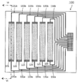
이와 같은 본 발명의 도전성 적층체 (10) 는, 패턴 배선이 형성된 투명 도전성 적층체의 형성에 적합하다. 도 5 는, 패턴 배선이 형성된 투명 도전성 적층체의 일 실시형태를 모식적으로 나타내는 평면도이고, 도 6 은 도 5 의 Ⅵ-Ⅵ 선에 있어서의 단면을 모식적으로 나타내는 단면도이다. 패턴 배선이 형성된 투명 도전성 적층체 (100) 는, 패턴화된 복수의 투명 전극 (121 ∼ 126) 으로 이루어지는 투명 전극부, 및 패턴 배선부 (131a ∼ 136a, 131b ∼ 136b) 를 갖는다. 패턴 배선은, 각 투명 전극에 접속되어 있다. 예를 들어 도 5 의 투명 전극부 (121) 는, 패턴 배선 (131a 및 131b) 과 접속되어 있다. 도 6 에 모식적으로 나타내는 바와 같이, 투명 전극 (121) 은, 투명 기재 (1) 상에 투명 도전성 박막 적층체 (2) 를 갖는 영역이고, 패턴 배선 (131a 및 131b) 은, 투명 기재 (1) 상에 투명 도전성 박막 적층체 (2) 및 금속층 (3) 을 이 순서로 갖는 영역이다. 또한, 도 5 에 있어서는, 각 투명 전극이 단책상으로 패턴화되어 있고, 그 양단부가 패턴 배선과 접속되어 있지만, 투명 전극의 형상은 단책상에 한정되지 않고, 또, 투명 전극은 1 개 지점 또는 3 개 지점 이상에서 패턴 배선과 접속되어 있어도 된다. 각 패턴 배선은 필요에 따라, IC 등의 제어 수단 (150) 에 접속된다.Such a
이와 같은 패턴 배선이 형성된 투명 도전성 적층체는, 상기 도전성 적층체의 투명 도전성 박막 적층체 (2) 및 금속층 (3) 을 에칭 등에 의해 제거하여 패턴화함으로써 형성될 수 있다. 구체적으로는, 먼저, 금속층 (3) 의 면내의 일부가 제거되어, 패턴 배선이 형성된다. 이 때, 패턴 배선부 (131a ∼ 136a 및 131b ∼ 136b) 에 있어서 금속층 (3) 이 잔존하도록 가공이 실시된다. 또, 도 7 에 모식적으로 나타내는 바와 같이, 투명 전극과 패턴 배선의 접속부 (231a ∼ 236a 및 231b ∼ 236b) 에 있어서도 금속층 (3) 이 잔존하도록, 가공이 실시되는 것이 바람직하다. 또한, 이 패턴 배선과 투명 전극의 접속부는 패턴 배선부의 일부를 구성하고 있다.The transparent conductive laminate with such pattern wiring can be formed by removing and patterning the transparent conductive
금속층 (3) 의 제거는, 에칭에 의해 실시하는 것이 바람직하다. 에칭시에는, 패턴을 형성하기 위한 마스크에 의해 패턴 배선부 및 접속부에 대응하는 영역의 표면을 덮고, 에천트에 의해 금속층 (3) 을 에칭하는 방법이 바람직하게 사용된다. 또한, 금속층 상에 산화 방지 등을 목적으로 하여 제 2 금속층 (4) 이 형성되어 있는 경우에는, 1 회의 에칭 가공에 의해, 금속층 (3) 과 제 2 금속층 (4) 이 동시에 제거되는 것이 바람직하다. 에천트로는, 염화 제2구리 용액, 염화 제2철 용액, 구리암모니아 착물 용액 등을 들 수 있다. 그 중에서도, 투명 도전성 박막에 대해 에칭 능력을 나타내지 않는 에천트, 또는 투명 도전성 박막에 대한 에칭 속도가 금속층에 대한 에칭 속도에 비교하여 작은 에천트가 바람직하게 사용된다.It is preferable to remove the
금속층 (3) 을 제거한 후, 투명 도전성 박막 적층체 (2) 의 노출부에 있어서, 투명 도전성 박막 적층체 (2) 의 면내의 일부가 제거됨으로써, 도 5 에 나타내는 바와 같은 패턴화된 투명 전극 (121 ∼ 126) 이 형성된다. 투명 도전성 박막 적층체 (2) 의 제거도 에칭에 의해 실시하는 것이 바람직하다. 에칭시에는, 패턴을 형성하기 위한 마스크에 의해, 투명 전극부 (121 ∼ 126) 에 대응하는 영역의 표면을 덮고, 에천트에 의해 투명 도전성 박막 적층체를 에칭하는 방법이 바람직하게 사용된다. 또, 금속층 (3) 에 대해서도 에칭 능력을 갖는 에천트가 사용되는 경우에는, 상기 패턴 배선부 및 접속부도 마스크에 의해 표면이 덮이는 것이 바람직하다.After removing the
투명 도전성 박막의 에칭에 사용되는 에천트는, 투명 도전성 박막을 형성하는 재료에 따라 적절히 선택할 수 있다. 투명 도전성 박막으로서 ITO 등의 도전성 산화물이 사용되는 경우에는, 에천트로서 산이 바람직하게 사용된다. 산으로는, 예를 들어, 염화수소, 브롬화수소, 황산, 질산, 인산 등의 무기산, 아세트산 등의 유기산, 및 이들의 혼합물, 그리고 그들의 수용액을 들 수 있다.The etchant used for etching the transparent conductive thin film can be appropriately selected depending on the material forming the transparent conductive thin film. When a conductive oxide such as ITO is used as the transparent conductive thin film, an acid is preferably used as an etchant. Examples of the acid include inorganic acids such as hydrogen chloride, hydrogen bromide, sulfuric acid, nitric acid and phosphoric acid, organic acids such as acetic acid, and mixtures thereof, and aqueous solutions thereof.
또한, 투명 도전성 박막이 비정질인 경우는, 대기 중 등의 산소 존재 하에서 가열함으로써 결정화해도 된다. 결정화 조건은 적절히 설정할 수 있는데, 투명 도전성 박막이 ITO 로 형성되는 경우에는, 예를 들어, 100 ℃ ∼ 180 ℃ 의 온도 범위에서 15 분 ∼ 180 분 정도 가열을 실시하면 된다. 투명 도전성 박막이 결정질이라는 것은, 투과형 전자 현미경 (TEM) 관찰로, 결정화된 그레인이 전체면에 존재하는 상태를 가리킨다. 또, 투명 도전성 박막이 ITO 로 형성되는 경우에는, 적층체를 농도 5 wt% 의 염산에 15 분간 침지시킨 후, 수세·건조시키고, 15 ㎜ 사이의 단자간 저항을 테스터로 측정함으로써도 결정질인지의 여부를 판단할 수 있다. 비정질 ITO 막은 염산에 의해 에칭되어 소실되기 때문에, 염산으로의 침지에 의해 저항이 증대된다. 본 명세서에 있어서는, 염산으로의 침지·수세·건조 후에, 15 ㎜ 사이의 단자간 저항이 10 ㏀ 을 초과하는 경우에, ITO 막이 비정질인 것으로 한다.Moreover, when a transparent conductive thin film is amorphous, you may crystallize by heating in presence of oxygen, such as in air. The crystallization conditions can be appropriately set. When the transparent conductive thin film is formed of ITO, heating may be performed for about 15 minutes to 180 minutes in a temperature range of 100°C to 180°C, for example. The fact that the transparent conductive thin film is crystalline refers to a state in which crystallized grains are present on the entire surface by observation of a transmission electron microscope (TEM). Also, when the transparent conductive thin film is formed of ITO, the laminate is immersed in hydrochloric acid having a concentration of 5 wt% for 15 minutes, washed with water and dried, and the interterminal resistance between 15 mm is measured by a tester. Can determine whether Since the amorphous ITO film is etched away with hydrochloric acid and disappears, resistance is increased by immersion in hydrochloric acid. In this specification, it is assumed that the ITO film is amorphous when the resistance between terminals between 15 mm exceeds 10 MPa after immersion, water washing, and drying in hydrochloric acid.
투명 도전성 박막의 결정화는, 금속층의 제거에 의한 패턴 배선 형성 전, 패턴 배선 형성 후 투명 도전성 박막 적층체의 제거에 의한 투명 전극 형성 전, 투명 전극 형성 후의 어느 단계에서 실시해도 된다.The crystallization of the transparent conductive thin film may be performed at any stage before forming the pattern wiring by removing the metal layer, before forming the transparent electrode by removing the transparent conductive thin film laminate after forming the pattern wiring, and after forming the transparent electrode.
본 발명의 도전성 적층체는, 투명 도전성 박막 적층체 (2) 의 금속층 (3) 측의 투명 도전성 박막 (21) 으로서 불순물 금속의 함유비가 상대적으로 큰 복합 금속 산화물이 사용되고 있기 때문에, 금속층 (3) 을 에칭에 의해 제거한 후의 투명 도전성 박막 적층체의 표면 저항의 상승이 억제된다. 그 때문에, 저저항의 투명 전극을 갖는 패턴 배선이 형성된 투명 도전성 적층체를, 높은 생산성으로 얻을 수 있다.In the conductive laminate of the present invention, since the composite metal oxide having a relatively large content of impurity metal is used as the transparent conductive
<광학 디바이스> <optical device>
이와 같이 하여 얻어진 패턴 배선이 형성된 투명 도전성 적층체는, 필요에 따라 기판 상에 IC 등의 제어 수단 (150) 이 형성되어, 실용에 제공된다. 본 발명의 투명 도전성 적층체는, 패턴화된 투명 전극을 갖고, 각 투명 전극이 패턴 배선에 접속되어 있기 때문에, 각종의 광학 디바이스에 바람직하게 사용된다. 이와 같은 디바이스로는, 터치 패널이나, 액정 디스플레이, 플라즈마 디스플레이, 유기 EL 디스플레이 등의 플랫 패널 디스플레이, 조명 장치 등을 들 수 있다. 터치 패널로는, 예를 들어, 정전 용량 방식, 저항막 방식 등의 터치 패널을 들 수 있다.The transparent conductive laminated body in which the pattern wiring obtained in this way is formed is provided with control means 150, such as an IC, on a board|substrate as needed, and is provided for practical use. Since the transparent conductive laminate of the present invention has a patterned transparent electrode and each transparent electrode is connected to a pattern wiring, it is preferably used for various optical devices. Examples of such devices include touch panels, flat panel displays such as liquid crystal displays, plasma displays, and organic EL displays, and lighting devices. As the touch panel, for example, a touch panel such as an electrostatic capacitive method or a resistive film method can be used.
이와 같은 광학 디바이스의 형성에 있어서는, 패턴 배선이 형성된 투명 도전성 적층체를 그대로 사용해도 되고, 투명 전극 상에 다른 부가적인 층을 형성한 것을 사용할 수 있다. 예를 들어 유기 EL 에서는, 양극으로서 작용할 수 있는 투명 전극 상에, 발광층, 및 음극으로서 작용할 수 있는 금속 전극층 등을 형성할 수 있다.In the formation of such an optical device, a transparent conductive laminate in which pattern wiring is formed may be used as it is, or one in which another additional layer is formed on the transparent electrode can be used. For example, in the organic EL, a light emitting layer and a metal electrode layer that can act as a cathode can be formed on a transparent electrode that can act as an anode.
실시예Example
이하, 본 발명의 도전성 적층체에 관해서, 실시예를 사용하여 상세하게 설명하는데, 본 발명은 그 요지를 넘지 않는 한, 실시예에 한정되는 것은 아니다.Hereinafter, the conductive laminate of the present invention will be described in detail using examples, but the present invention is not limited to the examples as long as the gist is not exceeded.
[실시예 1] [Example 1]
(투명 도전성 필름의 제작) (Preparation of transparent conductive film)
두께 75 ㎛ 의 폴리카보네이트계 필름으로 이루어지는 필름 기재의 일방의 면에, 광경화형 수지 (JSR 제조 상품명 「옵스타 KZ6661」) 를 사용하여 두께 100 ㎚ 의 유전체층을 형성하였다. Ar 및 O2 를 도입한 감압 하에서, 산화인듐과 산화주석을 90 : 10 의 중량비로 갖는 소결체의 타깃 재료를 사용하여, DC 마그네트론 스퍼터법에 의해, 유전체층 상에 Sn 과 In 의 원자수 비 Sn/In 이 0.10 인 인듐-주석 복합 산화물로 이루어지는 제 2 투명 도전성 박막을 20 ㎚ 의 두께로 형성하였다. 이 박막 상에, 산화인듐과 산화주석을 97 : 3 의 중량비로 갖는 소결체의 타깃 재료를 사용하여, DC 마그네트론 스퍼터법에 의해, Sn 과 In 의 원자수 비 Sn/In 이 0.03 의 인듐-주석 복합 산화물로 이루어지는 제 1 투명 도전성 박막을 6 ㎚ 의 두께로 형성하였다. 이와 같이 하여, 폴리카보네이트 필름 기재 상에, Sn/In=0.10 이고 두께가 20 ㎚ 인 ITO 막 및 Sn/In=0.03 이고 두께가 6 ㎚ 인 ITO 막으로 이루어지는 투명 도전성 박막 적층체를 갖는 투명 도전성 필름을 얻었다.A dielectric layer having a thickness of 100 nm was formed on one side of the film base material made of a 75 µm-thick polycarbonate film using a photo-curable resin (trade name "Opstar KZ6661" manufactured by JSR). Under the reduced pressure of introducing Ar and O 2 , using a target material of a sintered body having indium oxide and tin oxide in a weight ratio of 90:10, by using DC magnetron sputtering, the atomic number ratio of Sn and In on the dielectric layer Sn/ A second transparent conductive thin film composed of an In0-0.10 indium-tin composite oxide was formed to a thickness of 20 nm. On this thin film, using a target material of a sintered body having indium oxide and tin oxide in a weight ratio of 97: 3, the atomic number ratio Sn/In of Sn and In was 0.03 by an indium-tin composite by DC magnetron sputtering. A first transparent conductive thin film made of oxide was formed to a thickness of 6 nm. Thus, on the polycarbonate film substrate, a transparent conductive film having a transparent conductive thin film laminate composed of an ITO film having Sn/In=0.10 and a thickness of 20 nm and an ITO film having Sn/In=0.03 and a thickness of 6 nm. Got
(금속층의 형성) (Formation of metal layer)
이 투명 도전성 필름의 제 1 투명 도전성 박막 상에, Ar 을 도입한 감압 하에서, 무산소 구리 타깃을 사용하여, DC 마그네트론 스퍼터법에 의해, 구리로 이루어지는 금속층을 50 ㎚ 의 두께로 형성하여, 도전성 적층체를 얻었다.On the first transparent conductive thin film of this transparent conductive film, under a reduced pressure introduced with Ar, an oxygen-free copper target was used to form a metal layer made of copper to a thickness of 50 nm by a DC magnetron sputtering method, to form a conductive laminate. Got
[실시예 2] [Example 2]
두께 23 ㎛ 의 폴리에틸렌테레프탈레이트 필름으로 이루어지는 필름 기재의 일방의 면에, 멜라민 수지 : 알키드 수지 : 유기 실란 축합물의 중량비 2 : 2 : 1 의 열경화형 수지 (광의 굴절률 n=1.54) 를 사용하여 두께 35 ㎚ 의 유전체층을 형성하였다. 이 유전체층 상에, 실시예 1 과 동일하게 하여, Sn/In=0.10 이고 두께가 20 ㎚ 인 ITO 막 (제 2 투명 도전성 박막) 및 Sn/In=0.03 이고 두께가 6 ㎚ 인 ITO 막 (제 1 투명 도전성 박막) 을 순차 형성하여, 투명 도전성 필름을 얻었다. 이 투명 도전성 필름의 제 1 투명 도전성 박막 상에, 실시예 1 과 동일하게 하여 구리로 이루어지는 금속층을 50 ㎚ 의 두께로 형성하여, 도전성 적층체를 얻었다.35 on the one side of the film base material made of a polyethylene terephthalate film having a thickness of 23 µm, using a thermosetting resin (light refractive index n=1.54) having a weight ratio of 2:2:1 to melamine resin:alkyd resin:organic silane condensate. A dielectric layer of nm was formed. On this dielectric layer, in the same manner as in Example 1, an ITO film having Sn/In=0.10 and a thickness of 20 nm (second transparent conductive thin film) and an ITO film having Sn/In=0.03 and a thickness of 6 nm (first part) A transparent conductive thin film) was sequentially formed to obtain a transparent conductive film. On the first transparent conductive thin film of this transparent conductive film, a metal layer made of copper was formed to a thickness of 50 nm in the same manner as in Example 1 to obtain a conductive laminate.
[실시예 3] [Example 3]
두께 50 ㎛ 의 폴리에틸렌테레프탈레이트 필름으로 이루어지는 필름 기재의 일방의 면에, 실시예 2 와 동일하게 유전체층을 형성하였다. 이 유전체층 상에, 실시예 1 과 동일하게 하여, Sn/In=0.10 이고 두께가 26 ㎚ 인 ITO 막 및 Sn/In=0.03 이고 두께가 2 ㎚ 인 ITO 막을 순차 형성하여, 투명 도전성 필름을 얻었다. 이 투명 도전성 필름의 제 1 투명 도전성 박막 상에, 실시예 1 과 동일하게 하여 구리로 이루어지는 금속층을 50 ㎚ 의 두께로 형성하여, 도전성 적층체를 얻었다.A dielectric layer was formed in the same manner as in Example 2 on one side of the film base material made of a polyethylene terephthalate film having a thickness of 50 µm. On this dielectric layer, in the same manner as in Example 1, an ITO film having Sn/In=0.10 and a thickness of 26 nm and an ITO film having Sn/In=0.03 and a thickness of 2 nm were sequentially formed to obtain a transparent conductive film. On the first transparent conductive thin film of this transparent conductive film, a metal layer made of copper was formed to a thickness of 50 nm in the same manner as in Example 1 to obtain a conductive laminate.
[실시예 4 ∼ 10, 비교예 4] [Examples 4 to 10 and Comparative Example 4]
ITO 막의 형성에 사용하는 타깃의 산화인듐과 산화주석의 비율, 및 제막 두께를 표 1 에 나타내는 바와 같이 변경한 것 이외에는, 실시예 3 과 동일하게 하여, 도전성 적층체를 얻었다.A conductive laminate was obtained in the same manner as in Example 3, except that the ratio of indium oxide and tin oxide of the target used for forming the ITO film and the film thickness were changed as shown in Table 1.
[비교예 1] [Comparative Example 1]
두께 50 ㎛ 의 폴리에틸렌테레프탈레이트 필름으로 이루어지는 필름 기재의 일방의 면에, 실시예 2 와 동일하게 유전체층을 형성하였다. Ar 및 O2 를 도입한 감압 하에서, 산화인듐과 산화주석을 90 : 10 의 중량비로 갖는 소결체의 타깃 재료를 사용하여, DC 마그네트론 스퍼터법에 의해, 유전체층 상에 Sn 과 In 의 원자수 비 Sn/In 이 0.10 인 인듐-주석 복합 산화물로 이루어지는 투명 도전성 박막을 20 ㎚ 의 두께로 형성하여, 기재 상에 투명 도전성 박막을 1 층만 갖는 투명 도전성 필름을 얻었다. 이 투명 도전성 필름의 투명 도전성 박막 상에, 실시예 1 과 동일하게 하여 구리로 이루어지는 금속층을 50 ㎚ 의 두께로 형성하여, 도전성 적층체를 얻었다.A dielectric layer was formed in the same manner as in Example 2 on one side of the film base material made of a polyethylene terephthalate film having a thickness of 50 µm. Under the reduced pressure of introducing Ar and O 2 , using a target material of a sintered body having indium oxide and tin oxide in a weight ratio of 90:10, by using DC magnetron sputtering, the atomic number ratio of Sn and In on the dielectric layer Sn/ A transparent conductive thin film made of In0.0.1 indium-tin composite oxide was formed to a thickness of 20 nm to obtain a transparent conductive film having only one layer of a transparent conductive thin film on a substrate. On the transparent conductive thin film of this transparent conductive film, in the same manner as in Example 1, a metal layer made of copper was formed to a thickness of 50 nm to obtain a conductive laminate.
[비교예 2] [Comparative Example 2]
실시예 3 과 동일하게, 두께 50 ㎛ 의 폴리에틸렌테레프탈레이트 필름 기재의 일방의 면에 유전체층을 형성하였다. 이 유전체층 상에, 비교예 1 과 동일하게 하여, Sn/In 비가 0.08 인 ITO 막을 막두께 25 ㎚ 로 형성하고, 그 위에 구리로 이루어지는 금속층을 50 ㎚ 의 두께로 형성하여, 도전성 적층체를 얻었다.In the same manner as in Example 3, a dielectric layer was formed on one side of a polyethylene terephthalate film substrate having a thickness of 50 µm. On this dielectric layer, in the same manner as in Comparative Example 1, an ITO film having an Sn/In ratio of 0.08 was formed with a film thickness of 25 nm, and a metal layer made of copper was formed thereon with a thickness of 50 nm to obtain a conductive laminate.
[비교예 3] [Comparative Example 3]
상기 비교예 2 에 있어서, ITO 막의 형성에 사용하는 타깃의 산화인듐과 산화주석의 중량비를 88 : 12 (ITO 막의 Sn/In 비=0.13) 로 변경한 것 이외에는, 비교예 2 와 동일하게 하여, 도전성 적층체를 얻었다.In Comparative Example 2, except for changing the weight ratio of indium oxide and tin oxide of the target used for the formation of the ITO film to 88: 12 (Sn/In ratio of ITO film = 0.13), it was carried out in the same manner as in Comparative Example 2, A conductive laminate was obtained.
<평가> <Evaluation>
실온 하에서, 암모니아 수용액 (농도 8 중량%) 100 중량부에 대해 염화암모늄 8 중량부를 혼합한 용액 (에천트) 에, 각 실시예 및 비교예에서 얻어진 도전성 적층체를 10 분간 침지시켜, 구리층을 에칭 제거하였다.Under room temperature, a conductive layered product obtained in each Example and Comparative Example was immersed in a solution (etchant) in which 8 parts by weight of ammonium chloride was mixed with 100 parts by weight of an aqueous ammonia solution (concentration 8% by weight) for 10 minutes, and the copper layer was The etching was removed.
구리층을 형성하기 전의 투명 도전성 필름 및 도전성 적층체로부터 구리층을 에칭에 의해 제거한 투명 도전성 필름의 각각을, 140 ℃ 의 열풍 오븐에서 90 분간 가열하여, ITO 의 결정화를 실시하였다. 결정화 후의 도전성 박막 (적층체) 의 표면 저항을 4 단자법에 의해 측정하였다.Each of the transparent conductive films from which the copper layers were removed by etching from the transparent conductive film and the conductive laminate before forming the copper layer was heated in a hot air oven at 140°C for 90 minutes to crystallize ITO. The surface resistance of the conductive thin film (laminate) after crystallization was measured by a four-terminal method.
각 실시예 및 비교예의 ITO 막의 제막에 사용한 타깃 중의 산화인듐과 산화주석의 합계에 대한 산화주석의 양 (중량%), ITO 막 중의 Sn/In 비, 및 구리층을 에칭에 의해 제거하는 전후에서의 표면 저항을 표 1 에 나타낸다. 표 1 중, ITO1 은, 제 1 투명 도전성 박막 (금속층측의 ITO 막), ITO2 는, 제 2 투명 도전성 박막 (기재측의 ITO 막) 을 나타낸다.Before and after removing the amount of tin oxide (% by weight), the Sn/In ratio in the ITO film, and the copper layer by etching with respect to the sum of indium oxide and tin oxide in the target used for forming the ITO film of each of the Examples and Comparative Examples. Table 1 shows the surface resistance. In Table 1, ITO1 represents a 1st transparent conductive thin film (ITO film on a metal layer side), and ITO2 represents a 2nd transparent conductive thin film (ITO film on a substrate side).

기재 상에 투명 도전성 박막을 1 층만 갖는 비교예 1 ∼ 3 에서는, 구리층을 형성 후에 에칭 제거한 경우의 표면 저항이, 구리층 형성 전에 비하여 약 8 % ∼ 13 % 증가되어 있었다. 또, 금속층측의 투명 도전성 박막 (ITO1) 에 있어서의 불순물 금속 (Sn) 의 함유비가, 기재측의 투명 도전성 박막 (ITO2) 보다 큰 비교예 2 에 있어서도, 표면 저항의 증가가 보여졌다. 이에 반하여, 실시예 1 ∼ 10 에서는, 구리층을 에칭 제거한 후에도 저항의 변화가 작았다. 이 점에서, Sn 함유량이 작은 제 1 투명 도전성 박막을 형성함으로써, 저항의 증가가 억제되는 것을 알 수 있다.In Comparative Examples 1-3 having only one layer of a transparent conductive thin film on the substrate, the surface resistance when etching was removed after the copper layer was formed was increased by about 8% to 13% compared to before the copper layer was formed. Further, in Comparative Example 2 in which the content ratio of the impurity metal (Sn) in the transparent conductive thin film (ITO1) on the metal layer side was larger than that in the transparent conductive thin film (ITO2) on the substrate side, an increase in surface resistance was observed. In contrast, in Examples 1 to 10, the change in resistance was small even after the copper layer was etched and removed. From this point, it can be seen that the increase in resistance is suppressed by forming the first transparent conductive thin film having a small Sn content.
1 : 투명 기재
2 : 투명 도전성 박막 적층체
21, 22, 23, 25 : 투명 도전성 박막
3, 4 : 금속층
10 : 도전성 적층체
100 : 투명 도전성 적층체
121 ∼ 126 : 투명 전극
131 ∼ 136 : 패턴 배선
231 ∼ 236 : 접속부
150 : 제어 수단1: Transparent substrate
2: Transparent conductive thin film laminate
21, 22, 23, 25: Transparent conductive thin film
3, 4: metal layer
10: conductive laminate
100: transparent conductive laminate
121 to 126: transparent electrode
131 136: pattern wiring
231 236: Connection
150: control means
Claims (16)
상기 투명 도전성 박막 적층체에 있어서, 상기 금속층에 가장 근접한 제 1 투명 도전성 박막은, 금속 산화물층 또는 주금속과 1 종 이상의 불순물 금속을 함유하는 복합 금속 산화물층이고, 제 1 투명 도전성 박막 이외의 투명 도전성 박막은, 주금속과 1 종 이상의 불순물 금속을 함유하는 복합 금속 산화물층이고,
상기 제 1 투명 도전성 박막에 있어서의 불순물 금속의 함유비가, 상기 투명 도전성 박막 적층체를 구성하는 다른 어떤 투명 도전성 박막에 있어서의 불순물 금속의 함유비보다 작고,
상기 투명 도전성 박막 적층체를 구성하는 모든 투명 도전성 박막이 결정질막인, 도전성 적층체.A transparent conductive thin film laminate made of at least two layers of transparent conductive thin films and a metal layer formed on the surface of at least one of the transparent substrates in this order,
In the transparent conductive thin film laminate, the first transparent conductive thin film closest to the metal layer is a metal oxide layer or a composite metal oxide layer containing a main metal and at least one impurity metal, and is transparent other than the first transparent conductive thin film. The conductive thin film is a composite metal oxide layer containing a main metal and at least one impurity metal,
The content ratio of the impurity metal in the first transparent conductive thin film is smaller than the content ratio of the impurity metal in any other transparent conductive thin film constituting the transparent conductive thin film laminate,
A conductive laminate in which all the transparent conductive thin films constituting the transparent conductive thin film laminate are crystalline films.
상기 투명 도전성 박막 적층체 중에서 가장 불순물 금속의 함유비가 큰 투명 도전성 박막에 있어서의 불순물 금속의 함유비와, 상기 제 1 투명 도전성 박막에 있어서의 불순물 금속의 함유비의 차가, 0.005 ∼ 0.23 인, 도전성 적층체.According to claim 1,
The difference between the content ratio of the impurity metal in the transparent conductive thin film and the content ratio of the impurity metal in the first transparent conductive thin film is 0.005 to 0.23. Laminate.
상기 제 1 투명 도전성 박막에 있어서의 불순물 금속의 함유비가 0.08 이하인, 도전성 적층체.According to claim 1,
The conductive laminated body in which the content ratio of the impurity metal in the first transparent conductive thin film is 0.08 or less.
상기 투명 도전성 박막 적층체 중에서 가장 불순물 금속의 함유비가 높은 투명 도전성 박막에 있어서의 불순물 금속의 함유비가 0.04 ∼ 0.31 인, 도전성 적층체.According to claim 1,
The conductive laminated body in which the content ratio of the impurity metal in the transparent conductive thin film having the highest content ratio of impurity metal among the transparent conductive thin film laminates is 0.04 to 0.31.
상기 제 1 투명 도전성 박막의 두께가, 투명 도전성 박막 적층체의 전체의 두께에 대해 6 % 이상인, 도전성 적층체.According to claim 1,
The thickness of the said first transparent conductive thin film is 6% or more with respect to the whole thickness of the transparent conductive thin film laminated body, The conductive laminated body.
상기 투명 도전성 박막 적층체를 구성하는 모든 투명 도전성 박막은, 주금속이 In 인, 도전성 적층체.According to claim 1,
All of the transparent conductive thin films constituting the transparent conductive thin film laminate have a main metal of In, which is a conductive laminate.
상기 투명 도전성 박막 적층체를 구성하는 모든 투명 도전성 박막은, 불순물 금속으로서 Sn 을 함유하는, 도전성 적층체.The method of claim 6,
All of the transparent conductive thin films constituting the transparent conductive thin film laminate include Sn as an impurity metal.
상기 제 1 투명 도전성 박막에 있어서의 In 에 대한 Sn 의 함유비가, 0.08 이하이고, 제 1 투명 도전성 박막 이외의 상기 투명 도전성 박막 적층체를 구성하는 투명 도전성 박막 전체에 있어서의 In 에 대한 Sn 의 함유비가, 0.08 ∼ 0.13 인, 도전성 적층체.The method of claim 7,
The content ratio of Sn to In in the first transparent conductive thin film is 0.08 or less, and the content of Sn to In in the entire transparent conductive thin film constituting the transparent conductive thin film laminate other than the first transparent conductive thin film The conductive laminate having a ratio of 0.08 to 0.13.
상기 투명 도전성 박막 적층체가, 상기 제 1 투명 도전성 박막 및 상기 제 1 투명 도전성 박막보다 기재측에 형성된 1 층의 투명 도전성 박막의 2 층으로 이루어지는, 도전성 적층체.According to claim 1,
The said transparent conductive thin film laminated body consists of two layers of the said 1st transparent conductive thin film and the 1st transparent conductive thin film formed on the substrate side rather than the said 1st transparent conductive thin film.
상기 제 1 투명 도전성 박막과 상기 금속층이 인접하고 있는, 도전성 적층체.According to claim 1,
A conductive laminate in which the first transparent conductive thin film and the metal layer are adjacent.
상기 투명 기재가 가요성 필름인, 도전성 적층체.According to claim 1,
A conductive laminate, wherein the transparent substrate is a flexible film.
상기 패턴 배선부는, 투명 기재 상에 적어도 2 층의 투명 도전성 박막으로 이루어지는 투명 도전성 박막 적층체 및 금속층을 이 순서로 갖고,
상기 투명 전극부는, 투명 기재 상에 상기 투명 도전성 박막 적층체를 갖고,
상기 투명 도전성 박막 적층체에 있어서, 상기 금속층에 가장 근접한 제 1 투명 도전성 박막에 있어서의 불순물 금속의 함유비가, 상기 투명 도전성 박막 적층체를 구성하는 다른 어떤 투명 도전성 박막에 있어서의 불순물 금속의 함유비보다 작고,
상기 투명 도전성 박막 적층체를 구성하는 모든 투명 도전성 박막이 결정질막인, 패턴 배선이 형성된 투명 도전성 적층체.A transparent conductive laminate having a transparent electrode portion and a pattern wiring portion formed of a plurality of patterned transparent electrodes on a transparent substrate, and a pattern wiring having a pattern wiring portion connected to each transparent electrode portion is formed.
The pattern wiring portion has a transparent conductive thin film laminate and a metal layer made of at least two transparent conductive thin films on a transparent substrate in this order,
The transparent electrode portion has the transparent conductive thin film laminate on a transparent substrate,
In the transparent conductive thin film laminate, the content ratio of the impurity metal in the first transparent conductive thin film closest to the metal layer is the content ratio of the impurity metal in any other transparent conductive thin film constituting the transparent conductive thin film laminate. Smaller than,
A transparent conductive laminate with patterned wiring, wherein all transparent conductive thin films constituting the transparent conductive thin film laminate are crystalline films.
상기 금속층이 제거된 투명 도전성 박막 적층체의 노출부에 있어서, 투명 도전성 박막 적층체의 면내의 일부를 에칭에 의해 제거하여 패턴화된 투명 전극을 형성함으로써 얻어질 수 있는 패턴 배선이 형성된 투명 도전성 적층체.A portion of the metal layer of the conductive laminate according to any one of claims 1 to 11 is removed by etching to form a pattern wiring portion,
In the exposed portion of the transparent conductive thin film laminate in which the metal layer is removed, a transparent conductive laminate in which pattern wiring can be obtained by removing a part of the surface of the transparent conductive thin film laminate by etching to form a patterned transparent electrode sieve.
제 1 항 내지 제 11 항 중 어느 한 항에 기재된 도전성 적층체를 준비하는 공정,
상기 금속층의 면내의 일부를 에칭에 의해 제거하여, 패턴 배선부를 형성하는 공정, 및
상기 금속층이 제거된 투명 도전성 박막 적층체의 노출부에 있어서, 투명 도전성 박막 적층체의 면내의 일부를 에칭에 의해 제거하여 패턴화된 투명 전극을 형성하는 공정을 이 순서로 갖는, 패턴 배선이 형성된 투명 도전성 적층체의 제조 방법.A method of manufacturing a transparent conductive laminate having a pattern wiring on which a pattern wiring is connected, each having a transparent electrode portion and a pattern wiring portion made of a plurality of patterned transparent electrodes on a transparent substrate,
A process for preparing the conductive laminate according to any one of claims 1 to 11,
The step of forming a pattern wiring part by removing a part of the metal layer by etching, and
In the exposed portion of the transparent conductive thin film laminate in which the metal layer is removed, a pattern wiring is formed, in this order, the process of removing a part of the surface of the transparent conductive thin film laminate by etching to form a patterned transparent electrode. Method of manufacturing a transparent conductive laminate.
Applications Claiming Priority (3)
| Application Number | Priority Date | Filing Date | Title |
|---|---|---|---|
| JP2011135436A JP5473990B2 (en) | 2011-06-17 | 2011-06-17 | A conductive laminate, a transparent conductive laminate with a patterned wiring, and an optical device. |
| JPJP-P-2011-135436 | 2011-06-17 | ||
| PCT/JP2012/065253 WO2012173192A1 (en) | 2011-06-17 | 2012-06-14 | Conductive laminate, transparent conductive laminate with patterned wiring, and optical device |
Related Parent Applications (1)
| Application Number | Title | Priority Date | Filing Date |
|---|---|---|---|
| KR1020197025318A Division KR20190103489A (en) | 2011-06-17 | 2012-06-14 | Conductive laminate, transparent conductive laminate with patterned wiring, and optical device |
Publications (1)
| Publication Number | Publication Date |
|---|---|
| KR20200078719A true KR20200078719A (en) | 2020-07-01 |
Family
ID=47357173
Family Applications (5)
| Application Number | Title | Priority Date | Filing Date |
|---|---|---|---|
| KR1020207018480A KR20200078719A (en) | 2011-06-17 | 2012-06-14 | Conductive laminate, transparent conductive laminate with patterned wiring, and optical device |
| KR1020187008395A KR20180032695A (en) | 2011-06-17 | 2012-06-14 | Conductive laminate, transparent conductive laminate with patterned wiring, and optical device |
| KR1020157036691A KR102018414B1 (en) | 2011-06-17 | 2012-06-14 | Conductive laminate, transparent conductive laminate with patterned wiring, and optical device |
| KR1020137030243A KR20140009493A (en) | 2011-06-17 | 2012-06-14 | Conductive laminate, transparent conductive laminate with patterned wiring, and optical device |
| KR1020197025318A KR20190103489A (en) | 2011-06-17 | 2012-06-14 | Conductive laminate, transparent conductive laminate with patterned wiring, and optical device |
Family Applications After (4)
| Application Number | Title | Priority Date | Filing Date |
|---|---|---|---|
| KR1020187008395A KR20180032695A (en) | 2011-06-17 | 2012-06-14 | Conductive laminate, transparent conductive laminate with patterned wiring, and optical device |
| KR1020157036691A KR102018414B1 (en) | 2011-06-17 | 2012-06-14 | Conductive laminate, transparent conductive laminate with patterned wiring, and optical device |
| KR1020137030243A KR20140009493A (en) | 2011-06-17 | 2012-06-14 | Conductive laminate, transparent conductive laminate with patterned wiring, and optical device |
| KR1020197025318A KR20190103489A (en) | 2011-06-17 | 2012-06-14 | Conductive laminate, transparent conductive laminate with patterned wiring, and optical device |
Country Status (7)
| Country | Link |
|---|---|
| US (1) | US9674946B2 (en) |
| EP (1) | EP2722853B1 (en) |
| JP (1) | JP5473990B2 (en) |
| KR (5) | KR20200078719A (en) |
| CN (1) | CN103608872B (en) |
| TW (2) | TWI551925B (en) |
| WO (1) | WO2012173192A1 (en) |
Families Citing this family (34)
| Publication number | Priority date | Publication date | Assignee | Title |
|---|---|---|---|---|
| JP5473990B2 (en) | 2011-06-17 | 2014-04-16 | 日東電工株式会社 | A conductive laminate, a transparent conductive laminate with a patterned wiring, and an optical device. |
| JP2014164882A (en) * | 2013-02-22 | 2014-09-08 | Dainippon Printing Co Ltd | Laminate having excellent reliability and workability and method for producing laminate |
| JP3183365U (en) * | 2013-02-25 | 2013-05-16 | ファナック株式会社 | Rotating table of machine tool |
| JP6207846B2 (en) | 2013-03-04 | 2017-10-04 | 富士フイルム株式会社 | Transparent conductive film and touch panel |
| JP2014194720A (en) * | 2013-03-29 | 2014-10-09 | Dainippon Printing Co Ltd | Touch panel sensor, touch panel module and method for manufacturing touch panel sensor |
| KR20140122338A (en) | 2013-04-09 | 2014-10-20 | 쓰리엠 이노베이티브 프로퍼티즈 캄파니 | Touch Panel, Preparing Method Thereof, and Ag-Pd-Nd Alloy for Touch Panel |
| JP6275961B2 (en) | 2013-06-26 | 2018-02-07 | 富士フイルム株式会社 | Optical film and display device |
| CN104253165A (en) * | 2013-06-27 | 2014-12-31 | 海洋王照明科技股份有限公司 | Solar cell device and method for manufacturing same |
| US10338706B2 (en) * | 2013-11-27 | 2019-07-02 | Lg Chem, Ltd. | Conductive structure body precursor, conductive structure body and method for manufacturing the same |
| JP5917480B2 (en) * | 2013-12-09 | 2016-05-18 | アルプス電気株式会社 | Electrostatic sensor |
| JP5848786B2 (en) * | 2014-02-04 | 2016-01-27 | 日東電工株式会社 | A conductive laminate, a transparent conductive laminate with a patterned wiring, and an optical device. |
| KR102314238B1 (en) * | 2014-04-30 | 2021-10-18 | 닛토덴코 가부시키가이샤 | Transparent conductive film and method for producing same |
| CN106460153B (en) * | 2014-04-30 | 2019-05-10 | 日东电工株式会社 | Transparent and electrically conductive film and its manufacturing method |
| JP6211557B2 (en) | 2014-04-30 | 2017-10-11 | 日東電工株式会社 | Transparent conductive film and method for producing the same |
| TWI595507B (en) * | 2014-06-18 | 2017-08-11 | Geomatec Co Ltd | Laminates, methods of making the same, and electronic machines |
| WO2016002679A1 (en) * | 2014-06-30 | 2016-01-07 | 住友金属鉱山株式会社 | Conductive substrate, layered conductive substrate, method for producing conductive substrate, and method for producing layered conductive substrate |
| CN107112073B (en) * | 2014-12-26 | 2020-09-01 | 国立研究开发法人产业技术综合研究所 | Flexible conductive film and method for manufacturing same |
| JP5976970B1 (en) * | 2015-02-24 | 2016-08-24 | 日東電工株式会社 | Light transmissive film |
| EP3264233B1 (en) * | 2015-02-25 | 2019-02-27 | VTS-Touchsensor Co., Ltd. | Conductive laminated body for touch panel, and method for manufacturing conductive laminated body for touch panel |
| JP6698064B2 (en) * | 2015-03-04 | 2020-05-27 | 株式会社カネカ | Substrate with conductive layer, substrate with transparent electrode for touch panel, and methods for manufacturing the same |
| KR101999706B1 (en) | 2015-03-16 | 2019-07-12 | 주식회사 엘지화학 | Conductive structure body and electronic device comprising the same |
| JP6293368B2 (en) * | 2015-04-24 | 2018-03-14 | 株式会社アルバック | Transparent conductive substrate, manufacturing method thereof, and transparent conductive substrate manufacturing apparatus |
| KR102367249B1 (en) * | 2015-07-28 | 2022-02-25 | 삼성디스플레이 주식회사 | Flexible touch panel and method for manufacturing flexible touch panel |
| KR102587363B1 (en) * | 2015-07-31 | 2023-10-10 | 스미토모 긴조쿠 고잔 가부시키가이샤 | Conductive substrate and conductive substrate manufacturing method |
| JP6600550B2 (en) * | 2015-12-16 | 2019-10-30 | 日東電工株式会社 | Metal layer laminated transparent conductive film and touch sensor using the same |
| JP6617607B2 (en) * | 2016-02-29 | 2019-12-11 | 住友金属鉱山株式会社 | Film-forming method and method for manufacturing laminate substrate using the same |
| KR102159491B1 (en) | 2016-05-09 | 2020-09-24 | 주식회사 엘지화학 | A conductive transparent film |
| EP3545461A4 (en) * | 2016-11-24 | 2020-07-22 | Boe Technology Group Co. Ltd. | Flexible touch panel, flexible display panel and flexible display apparatus, and fabricating method thereof |
| CN109426397B (en) * | 2017-08-22 | 2020-08-04 | 京东方科技集团股份有限公司 | Preparation method of touch structure and touch structure |
| CN110096169B (en) * | 2018-01-30 | 2021-01-22 | 京东方科技集团股份有限公司 | Touch substrate, manufacturing method thereof and electronic device |
| JP7129830B2 (en) * | 2018-06-19 | 2022-09-02 | 日東電工株式会社 | Method for producing resin film, conductive film and laminated film |
| JP7114446B2 (en) * | 2018-11-28 | 2022-08-08 | 日東電工株式会社 | Conductive film and patterning method thereof |
| WO2021157494A1 (en) | 2020-02-03 | 2021-08-12 | 日東電工株式会社 | Transparent conductive layer, transparent conductive sheet, touch sensor, light control element, photoelectric conversion element, heat ray control member, antenna, electromagnetic wave shield member, and image display device |
| TWI824213B (en) * | 2020-12-19 | 2023-12-01 | 逢甲大學 | Flexible transparent conductive composite films and method of manufacturing the same |
Citations (1)
| Publication number | Priority date | Publication date | Assignee | Title |
|---|---|---|---|---|
| JPS63113585A (en) | 1986-10-06 | 1988-05-18 | アンダス・コーポレイション | Transparent electrode and making and use thereof |
Family Cites Families (24)
| Publication number | Priority date | Publication date | Assignee | Title |
|---|---|---|---|---|
| JPS63102928A (en) * | 1986-10-20 | 1988-05-07 | グンゼ株式会社 | Metallic film laminate |
| JPH0843841A (en) * | 1994-07-27 | 1996-02-16 | Toppan Printing Co Ltd | Formation of transparent conductive film |
| JPH11335815A (en) * | 1998-05-20 | 1999-12-07 | Nippon Sheet Glass Co Ltd | Substrate with transparent conductive film and deposition apparatus |
| US6743488B2 (en) | 2001-05-09 | 2004-06-01 | Cpfilms Inc. | Transparent conductive stratiform coating of indium tin oxide |
| JP4438381B2 (en) * | 2003-11-05 | 2010-03-24 | 株式会社ブリヂストン | Crystalline ITO film, method for crystallizing ITO film, transparent conductive film, touch panel, and dye-sensitized solar cell |
| JP2005244083A (en) * | 2004-02-27 | 2005-09-08 | Hayashi Junyaku Kogyo Kk | Etchant composition for conductive film |
| JP2005268616A (en) | 2004-03-19 | 2005-09-29 | Tosoh Corp | Transparent conductive film and manufacturing method |
| JP4528651B2 (en) * | 2005-03-01 | 2010-08-18 | 日東電工株式会社 | Transparent conductive film and touch panel |
| KR101244092B1 (en) | 2005-09-01 | 2013-03-18 | 이데미쓰 고산 가부시키가이샤 | Transparent conductive film, transparent electrode, and electrode base plate and manufacturing method of the same |
| JP4804867B2 (en) * | 2005-10-18 | 2011-11-02 | 出光興産株式会社 | Transparent conductive film, transparent electrode, electrode substrate and manufacturing method thereof |
| JP5101038B2 (en) | 2006-05-19 | 2012-12-19 | 株式会社フジクラ | Electrode substrate manufacturing method, electrode substrate evaluation method |
| JP4721359B2 (en) | 2006-09-12 | 2011-07-13 | 日東電工株式会社 | Transparent conductive laminate and touch panel provided with the same |
| JP4667471B2 (en) | 2007-01-18 | 2011-04-13 | 日東電工株式会社 | Transparent conductive film, method for producing the same, and touch panel provided with the same |
| JP4821670B2 (en) * | 2007-03-26 | 2011-11-24 | 旭硝子株式会社 | Method for manufacturing electrode substrate with auxiliary wiring |
| JP2009093911A (en) | 2007-10-09 | 2009-04-30 | Panasonic Corp | Transparent electrode and display with transparent electrode |
| KR101000057B1 (en) | 2008-02-04 | 2010-12-10 | 엘지전자 주식회사 | Solar Cell Having Multiple Transparent Conducting Layers And Manufacturing Method Thereof |
| JP4931858B2 (en) * | 2008-05-13 | 2012-05-16 | パナソニック株式会社 | Method for manufacturing organic electroluminescent device |
| JP5572932B2 (en) * | 2008-09-03 | 2014-08-20 | 凸版印刷株式会社 | Transparent conductive film and touch panel |
| US8269744B2 (en) * | 2008-09-05 | 2012-09-18 | Mitsubishi Electric Corporation | Touch screen, touch panel and display device |
| JP2010212085A (en) | 2009-03-10 | 2010-09-24 | Toppan Printing Co Ltd | Transparent conductive thin film |
| JP2011034806A (en) | 2009-07-31 | 2011-02-17 | Nissha Printing Co Ltd | Transparent conductive film with superior suitability for laminating, and touch panel using the same |
| JP5556436B2 (en) * | 2009-10-13 | 2014-07-23 | 東洋紡株式会社 | Transparent conductive laminated film, transparent conductive laminated sheet, and touch panel |
| JP2011154442A (en) * | 2010-01-26 | 2011-08-11 | Sony Corp | Sensor element and display apparatus |
| JP5473990B2 (en) | 2011-06-17 | 2014-04-16 | 日東電工株式会社 | A conductive laminate, a transparent conductive laminate with a patterned wiring, and an optical device. |
-
2011
- 2011-06-17 JP JP2011135436A patent/JP5473990B2/en active Active
-
2012
- 2012-06-14 KR KR1020207018480A patent/KR20200078719A/en not_active Application Discontinuation
- 2012-06-14 CN CN201280029923.9A patent/CN103608872B/en active Active
- 2012-06-14 EP EP12800306.8A patent/EP2722853B1/en not_active Not-in-force
- 2012-06-14 KR KR1020187008395A patent/KR20180032695A/en not_active Application Discontinuation
- 2012-06-14 KR KR1020157036691A patent/KR102018414B1/en active IP Right Grant
- 2012-06-14 WO PCT/JP2012/065253 patent/WO2012173192A1/en active Application Filing
- 2012-06-14 US US14/126,278 patent/US9674946B2/en active Active
- 2012-06-14 KR KR1020137030243A patent/KR20140009493A/en active Application Filing
- 2012-06-14 KR KR1020197025318A patent/KR20190103489A/en active Application Filing
- 2012-06-15 TW TW101121633A patent/TWI551925B/en active
- 2012-06-15 TW TW104113319A patent/TW201530238A/en unknown
Patent Citations (1)
| Publication number | Priority date | Publication date | Assignee | Title |
|---|---|---|---|---|
| JPS63113585A (en) | 1986-10-06 | 1988-05-18 | アンダス・コーポレイション | Transparent electrode and making and use thereof |
Also Published As
| Publication number | Publication date |
|---|---|
| CN103608872B (en) | 2017-12-26 |
| KR20190103489A (en) | 2019-09-04 |
| TW201305698A (en) | 2013-02-01 |
| US9674946B2 (en) | 2017-06-06 |
| TW201530238A (en) | 2015-08-01 |
| EP2722853B1 (en) | 2018-08-22 |
| WO2012173192A1 (en) | 2012-12-20 |
| CN103608872A (en) | 2014-02-26 |
| JP2013001009A (en) | 2013-01-07 |
| EP2722853A1 (en) | 2014-04-23 |
| EP2722853A4 (en) | 2015-02-25 |
| US20140102764A1 (en) | 2014-04-17 |
| KR20160005139A (en) | 2016-01-13 |
| KR20180032695A (en) | 2018-03-30 |
| KR102018414B1 (en) | 2019-09-04 |
| TWI551925B (en) | 2016-10-01 |
| JP5473990B2 (en) | 2014-04-16 |
| KR20140009493A (en) | 2014-01-22 |
Similar Documents
| Publication | Publication Date | Title |
|---|---|---|
| JP5473990B2 (en) | A conductive laminate, a transparent conductive laminate with a patterned wiring, and an optical device. | |
| KR102650752B1 (en) | Metal layer laminated transparent conductive film and touch sensor using the same | |
| JP5914036B2 (en) | Method for producing conductive laminated film | |
| CN102881357B (en) | Compound transparent electroconductive film | |
| KR101849449B1 (en) | Conductive structure body and method for manufacturing the same | |
| KR101671169B1 (en) | Metal mesh type touch screen panel and method of manufacturing the same | |
| JP6292225B2 (en) | Transparent conductor | |
| KR101241632B1 (en) | Method for manufacturing touch panel | |
| JP5848786B2 (en) | A conductive laminate, a transparent conductive laminate with a patterned wiring, and an optical device. | |
| JP6096869B2 (en) | Conductive laminate, transparent conductive laminate with pattern wiring, and optical device | |
| JP2015219690A (en) | Transparent conductive device and touch panel | |
| CN111240507A (en) | Conductive thin film and patterning method thereof | |
| KR101629665B1 (en) | Metal mesh type touch screen panel and method of manufacturing the same | |
| WO2015190227A1 (en) | Transparent conductor manufacturing method | |
| WO2014181538A1 (en) | Transparent conductor and method for producing same | |
| KR101940693B1 (en) | Conductive structure body and method for manufacturing the same | |
| KR20160069823A (en) | Conductive structure body and method for manufacturing the same |
Legal Events
| Date | Code | Title | Description |
|---|---|---|---|
| A107 | Divisional application of patent | ||
| E902 | Notification of reason for refusal | ||
| E601 | Decision to refuse application | ||
| J201 | Request for trial against refusal decision | ||
| J301 | Trial decision |
Free format text: TRIAL NUMBER: 2021101000886; TRIAL DECISION FOR APPEAL AGAINST DECISION TO DECLINE REFUSAL REQUESTED 20210408 Effective date: 20210714 |