KR20180098363A - 박막 트랜지스터와 이를 위한 제조 방법, 디스플레이 패널 및 디스플레이 장치 - Google Patents
박막 트랜지스터와 이를 위한 제조 방법, 디스플레이 패널 및 디스플레이 장치 Download PDFInfo
- Publication number
- KR20180098363A KR20180098363A KR1020187021458A KR20187021458A KR20180098363A KR 20180098363 A KR20180098363 A KR 20180098363A KR 1020187021458 A KR1020187021458 A KR 1020187021458A KR 20187021458 A KR20187021458 A KR 20187021458A KR 20180098363 A KR20180098363 A KR 20180098363A
- Authority
- KR
- South Korea
- Prior art keywords
- gate
- layer
- thin film
- film transistor
- protective layer
- Prior art date
- Legal status (The legal status is an assumption and is not a legal conclusion. Google has not performed a legal analysis and makes no representation as to the accuracy of the status listed.)
- Granted
Links
Images

Classifications
-
- H—ELECTRICITY
- H10—SEMICONDUCTOR DEVICES; ELECTRIC SOLID-STATE DEVICES NOT OTHERWISE PROVIDED FOR
- H10D—INORGANIC ELECTRIC SEMICONDUCTOR DEVICES
- H10D30/00—Field-effect transistors [FET]
- H10D30/60—Insulated-gate field-effect transistors [IGFET]
- H10D30/67—Thin-film transistors [TFT]
- H10D30/6704—Thin-film transistors [TFT] having supplementary regions or layers in the thin films or in the insulated bulk substrates for controlling properties of the device
-
- H—ELECTRICITY
- H10—SEMICONDUCTOR DEVICES; ELECTRIC SOLID-STATE DEVICES NOT OTHERWISE PROVIDED FOR
- H10D—INORGANIC ELECTRIC SEMICONDUCTOR DEVICES
- H10D30/00—Field-effect transistors [FET]
- H10D30/60—Insulated-gate field-effect transistors [IGFET]
- H10D30/67—Thin-film transistors [TFT]
-
- H01L29/78606—
-
- H01L27/3262—
-
- H01L29/06—
-
- H—ELECTRICITY
- H10—SEMICONDUCTOR DEVICES; ELECTRIC SOLID-STATE DEVICES NOT OTHERWISE PROVIDED FOR
- H10D—INORGANIC ELECTRIC SEMICONDUCTOR DEVICES
- H10D30/00—Field-effect transistors [FET]
- H10D30/01—Manufacture or treatment
- H10D30/021—Manufacture or treatment of FETs having insulated gates [IGFET]
- H10D30/031—Manufacture or treatment of FETs having insulated gates [IGFET] of thin-film transistors [TFT]
-
- H—ELECTRICITY
- H10—SEMICONDUCTOR DEVICES; ELECTRIC SOLID-STATE DEVICES NOT OTHERWISE PROVIDED FOR
- H10D—INORGANIC ELECTRIC SEMICONDUCTOR DEVICES
- H10D30/00—Field-effect transistors [FET]
- H10D30/60—Insulated-gate field-effect transistors [IGFET]
- H10D30/67—Thin-film transistors [TFT]
- H10D30/6758—Thin-film transistors [TFT] characterised by the insulating substrates
-
- H—ELECTRICITY
- H10—SEMICONDUCTOR DEVICES; ELECTRIC SOLID-STATE DEVICES NOT OTHERWISE PROVIDED FOR
- H10D—INORGANIC ELECTRIC SEMICONDUCTOR DEVICES
- H10D62/00—Semiconductor bodies, or regions thereof, of devices having potential barriers
- H10D62/10—Shapes, relative sizes or dispositions of the regions of the semiconductor bodies; Shapes of the semiconductor bodies
-
- H—ELECTRICITY
- H10—SEMICONDUCTOR DEVICES; ELECTRIC SOLID-STATE DEVICES NOT OTHERWISE PROVIDED FOR
- H10D—INORGANIC ELECTRIC SEMICONDUCTOR DEVICES
- H10D86/00—Integrated devices formed in or on insulating or conducting substrates, e.g. formed in silicon-on-insulator [SOI] substrates or on stainless steel or glass substrates
- H10D86/01—Manufacture or treatment
- H10D86/021—Manufacture or treatment of multiple TFTs
-
- H—ELECTRICITY
- H10—SEMICONDUCTOR DEVICES; ELECTRIC SOLID-STATE DEVICES NOT OTHERWISE PROVIDED FOR
- H10D—INORGANIC ELECTRIC SEMICONDUCTOR DEVICES
- H10D86/00—Integrated devices formed in or on insulating or conducting substrates, e.g. formed in silicon-on-insulator [SOI] substrates or on stainless steel or glass substrates
- H10D86/40—Integrated devices formed in or on insulating or conducting substrates, e.g. formed in silicon-on-insulator [SOI] substrates or on stainless steel or glass substrates characterised by multiple TFTs
- H10D86/451—Integrated devices formed in or on insulating or conducting substrates, e.g. formed in silicon-on-insulator [SOI] substrates or on stainless steel or glass substrates characterised by multiple TFTs characterised by the compositions or shapes of the interlayer dielectrics
-
- H—ELECTRICITY
- H10—SEMICONDUCTOR DEVICES; ELECTRIC SOLID-STATE DEVICES NOT OTHERWISE PROVIDED FOR
- H10D—INORGANIC ELECTRIC SEMICONDUCTOR DEVICES
- H10D86/00—Integrated devices formed in or on insulating or conducting substrates, e.g. formed in silicon-on-insulator [SOI] substrates or on stainless steel or glass substrates
- H10D86/40—Integrated devices formed in or on insulating or conducting substrates, e.g. formed in silicon-on-insulator [SOI] substrates or on stainless steel or glass substrates characterised by multiple TFTs
- H10D86/60—Integrated devices formed in or on insulating or conducting substrates, e.g. formed in silicon-on-insulator [SOI] substrates or on stainless steel or glass substrates characterised by multiple TFTs wherein the TFTs are in active matrices
-
- H—ELECTRICITY
- H10—SEMICONDUCTOR DEVICES; ELECTRIC SOLID-STATE DEVICES NOT OTHERWISE PROVIDED FOR
- H10K—ORGANIC ELECTRIC SOLID-STATE DEVICES
- H10K59/00—Integrated devices, or assemblies of multiple devices, comprising at least one organic light-emitting element covered by group H10K50/00
- H10K59/10—OLED displays
- H10K59/12—Active-matrix OLED [AMOLED] displays
- H10K59/121—Active-matrix OLED [AMOLED] displays characterised by the geometry or disposition of pixel elements
- H10K59/1213—Active-matrix OLED [AMOLED] displays characterised by the geometry or disposition of pixel elements the pixel elements being TFTs
-
- H—ELECTRICITY
- H10—SEMICONDUCTOR DEVICES; ELECTRIC SOLID-STATE DEVICES NOT OTHERWISE PROVIDED FOR
- H10K—ORGANIC ELECTRIC SOLID-STATE DEVICES
- H10K59/00—Integrated devices, or assemblies of multiple devices, comprising at least one organic light-emitting element covered by group H10K50/00
- H10K59/10—OLED displays
- H10K59/12—Active-matrix OLED [AMOLED] displays
- H10K59/124—Insulating layers formed between TFT elements and OLED elements
-
- H—ELECTRICITY
- H10—SEMICONDUCTOR DEVICES; ELECTRIC SOLID-STATE DEVICES NOT OTHERWISE PROVIDED FOR
- H10K—ORGANIC ELECTRIC SOLID-STATE DEVICES
- H10K77/00—Constructional details of devices covered by this subclass and not covered by groups H10K10/80, H10K30/80, H10K50/80 or H10K59/80
- H10K77/10—Substrates, e.g. flexible substrates
- H10K77/111—Flexible substrates
-
- H—ELECTRICITY
- H10—SEMICONDUCTOR DEVICES; ELECTRIC SOLID-STATE DEVICES NOT OTHERWISE PROVIDED FOR
- H10K—ORGANIC ELECTRIC SOLID-STATE DEVICES
- H10K2102/00—Constructional details relating to the organic devices covered by this subclass
- H10K2102/301—Details of OLEDs
- H10K2102/311—Flexible OLED
-
- Y—GENERAL TAGGING OF NEW TECHNOLOGICAL DEVELOPMENTS; GENERAL TAGGING OF CROSS-SECTIONAL TECHNOLOGIES SPANNING OVER SEVERAL SECTIONS OF THE IPC; TECHNICAL SUBJECTS COVERED BY FORMER USPC CROSS-REFERENCE ART COLLECTIONS [XRACs] AND DIGESTS
- Y02—TECHNOLOGIES OR APPLICATIONS FOR MITIGATION OR ADAPTATION AGAINST CLIMATE CHANGE
- Y02E—REDUCTION OF GREENHOUSE GAS [GHG] EMISSIONS, RELATED TO ENERGY GENERATION, TRANSMISSION OR DISTRIBUTION
- Y02E10/00—Energy generation through renewable energy sources
- Y02E10/50—Photovoltaic [PV] energy
- Y02E10/549—Organic PV cells
-
- Y—GENERAL TAGGING OF NEW TECHNOLOGICAL DEVELOPMENTS; GENERAL TAGGING OF CROSS-SECTIONAL TECHNOLOGIES SPANNING OVER SEVERAL SECTIONS OF THE IPC; TECHNICAL SUBJECTS COVERED BY FORMER USPC CROSS-REFERENCE ART COLLECTIONS [XRACs] AND DIGESTS
- Y02—TECHNOLOGIES OR APPLICATIONS FOR MITIGATION OR ADAPTATION AGAINST CLIMATE CHANGE
- Y02P—CLIMATE CHANGE MITIGATION TECHNOLOGIES IN THE PRODUCTION OR PROCESSING OF GOODS
- Y02P70/00—Climate change mitigation technologies in the production process for final industrial or consumer products
- Y02P70/50—Manufacturing or production processes characterised by the final manufactured product
Landscapes
- Engineering & Computer Science (AREA)
- Microelectronics & Electronic Packaging (AREA)
- Physics & Mathematics (AREA)
- Geometry (AREA)
- Thin Film Transistor (AREA)
- Electroluminescent Light Sources (AREA)
- Devices For Indicating Variable Information By Combining Individual Elements (AREA)
Abstract
Description
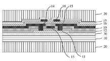
도 2는 본 발명의 일 실시예에 따른 다른 박막 트랜지스터의 개략 구조도이다.
12: 게이트 절연층 13: 게이트
14: 소스 15: 드레인
16: 패시베이션층 17: 평탄화층
18: 보호층 19: 층간 절연층
20: 상부 보호막 20: 하부 보호막
30: 배리어층
Claims (10)
- 박막 트랜지스터에 있어서,
플렉서블 기판 상에 순차적으로 형성된, 활성 영역, 게이트 절연층, 게이트, 소스 및 드레인, 패시베이션층 및 평탄화층을 구비하되, 보호층은 상기 패시베이션층과 상기 평탄화층 사이에 제공되고, 상기 보호층은 상기 활성 영역과 상기 게이트 바로 상측에 위치함을 특징으로 하는, 박막 트랜지스터.
- 제 1 항에 있어서,
상기 보호층은 상기 게이트에 수직인 방향으로 상기 게이트를 완전히 덮음을 특징으로 하는, 박막 트랜지스터.
- 제 1 항에 있어서,
상기 보호층은 유기 물질로 형성됨을 특징으로 하는, 박막 트랜지스터.
- 제 1 항에 있어서, 상기 보호층은 금속으로 형성됨을 특징으로 하는, 박막 트랜지스터.
- 제 4 항에 있어서,
상기 보호층은, 상기 게이트에 수직인 방향으로 상기 게이트와 상기 드레인 사이의 갭 뿐만 아니라 상기 게이트와 상기 소스 사이의 갭을 덮음을 특징으로 하는, 박막 트랜지스터.
- 제 1 항에 있어서,
상기 보호층의 영 계수(Young's modulus)는 300N/m2 보다 큼을 특징으로 하는, 박막 트랜지스터.
- 제 1 항 내지 제 6 항 중 어느 한 항에 있어서,
상부 보호막, 하부 보호막 및 배리어층(barrier layer)을 더 구비하되,
상기 상부 보호막은 상기 평탄화층 상측에 제공되고, 상기 하부 보호막은 상기 플렉서블 기판 하측에 제공되며, 상기 배리어층은 상기 플렉서블 기판과 상기 게이트 절연층 사이에 제공됨을 특징으로 하는, 박막 트랜지스터.
- 제 1 항 내지 제 7항 중 어느 한 항에서 설명한 박막 트랜지스터를 제조하는 방법에 있어서,
플렉서블 기판 상에 활성 영역, 게이트 절연층, 게이트, 소스 및 드레인, 그리고 패시베이션층을 순차적으로 형성하는 단계;
상기 패시베이션층 위에 보호층을 형성하는 단계; 및
상기 보호층 위에 평탄화층을 형성하는 단계를 구비하되,
상기 보호층은 상기 활성 영역과 상기 게이트 바로 상측에 위치함을 특징으로 하는, 방법.
- 제 1 항 내지 제 7 항 중 어느 한 항에서 설명한 박막 트랜지스터를 구비하는 디스플레이 패널.
- 제 9 항에서 설명한 디스플레이 패널을 구비하는 디스플레이 장치.
Applications Claiming Priority (3)
| Application Number | Priority Date | Filing Date | Title |
|---|---|---|---|
| CN201610111984.XA CN107134496B (zh) | 2016-02-29 | 2016-02-29 | 薄膜晶体管及其制造方法、显示面板及显示装置 |
| CN201610111984.X | 2016-02-29 | ||
| PCT/CN2017/075001 WO2017148348A1 (zh) | 2016-02-29 | 2017-02-27 | 薄膜晶体管及其制造方法、显示面板及显示装置 |
Publications (2)
| Publication Number | Publication Date |
|---|---|
| KR20180098363A true KR20180098363A (ko) | 2018-09-03 |
| KR102155434B1 KR102155434B1 (ko) | 2020-09-11 |
Family
ID=59721172
Family Applications (1)
| Application Number | Title | Priority Date | Filing Date |
|---|---|---|---|
| KR1020187021458A Active KR102155434B1 (ko) | 2016-02-29 | 2017-02-27 | 박막 트랜지스터와 이를 위한 제조 방법, 디스플레이 패널 및 디스플레이 장치 |
Country Status (7)
| Country | Link |
|---|---|
| US (1) | US10424667B2 (ko) |
| EP (1) | EP3425677B1 (ko) |
| JP (1) | JP6749400B2 (ko) |
| KR (1) | KR102155434B1 (ko) |
| CN (1) | CN107134496B (ko) |
| TW (1) | TWI673866B (ko) |
| WO (1) | WO2017148348A1 (ko) |
Families Citing this family (4)
| Publication number | Priority date | Publication date | Assignee | Title |
|---|---|---|---|---|
| CN108091612B (zh) * | 2017-12-07 | 2020-11-24 | 深圳市华星光电半导体显示技术有限公司 | 阵列基板及其制备方法 |
| CN108054291B (zh) * | 2017-12-28 | 2019-10-01 | 上海天马有机发光显示技术有限公司 | 一种柔性显示面板及其制备方法、柔性显示装置 |
| CN109887956B (zh) * | 2019-01-25 | 2021-04-27 | 武汉华星光电半导体显示技术有限公司 | 有机发光二极管柔性阵列基板 |
| TW202032226A (zh) * | 2020-01-14 | 2020-09-01 | 友達光電股份有限公司 | 軟性電路結構 |
Citations (7)
| Publication number | Priority date | Publication date | Assignee | Title |
|---|---|---|---|---|
| KR20040061656A (ko) * | 2002-12-31 | 2004-07-07 | 삼성전자주식회사 | 가요성 기판 상에 보호캡을 구비하는 박막 트랜지스터 및이를이용하는 전자장치 및 그 제조방법 |
| KR20080027185A (ko) * | 2006-09-22 | 2008-03-26 | 가부시키가이샤 한도오따이 에네루기 켄큐쇼 | 반도체장치 |
| EP2071627A2 (en) * | 2007-12-03 | 2009-06-17 | Semiconductor Energy Laboratory Co., Ltd. | Semiconductor device |
| JP2011171287A (ja) * | 2010-01-20 | 2011-09-01 | Semiconductor Energy Lab Co Ltd | フレキシブル発光装置、電子機器、及びフレキシブル発光装置の作製方法 |
| KR20130087915A (ko) * | 2012-01-30 | 2013-08-07 | 서울대학교산학협력단 | 박막 트랜지스터 및 이의 제조 방법 |
| KR20150026709A (ko) * | 2013-08-30 | 2015-03-11 | 엘지디스플레이 주식회사 | 플라스틱 유기전계 발광장치 및 그 제조방법 |
| US20150301195A1 (en) * | 2009-06-17 | 2015-10-22 | The Regents Of The University Of Michigan | Photodiode and other sensor structures in flat-panel x-ray imagers and method for improving topological uniformity of the photodiode and other sensor structures in flat-panel x-ray imagers based on thin-film electronics |
Family Cites Families (22)
| Publication number | Priority date | Publication date | Assignee | Title |
|---|---|---|---|---|
| US5828084A (en) * | 1995-03-27 | 1998-10-27 | Sony Corporation | High performance poly-SiGe thin film transistor |
| JP5350616B2 (ja) | 2006-09-22 | 2013-11-27 | 株式会社半導体エネルギー研究所 | 半導体装置 |
| KR101363835B1 (ko) * | 2007-02-05 | 2014-02-17 | 엘지디스플레이 주식회사 | 표시장치 및 이의 제조 방법 |
| US7973316B2 (en) * | 2007-03-26 | 2011-07-05 | Semiconductor Energy Laboratory Co., Ltd. | Semiconductor device and method for manufacturing semiconductor device |
| KR101298234B1 (ko) * | 2010-03-19 | 2013-08-22 | 엘지디스플레이 주식회사 | 터치인식 횡전계형 액정표시장치 및 이의 제조 방법 |
| KR101829313B1 (ko) * | 2011-11-03 | 2018-02-20 | 삼성디스플레이 주식회사 | 플렉서블 디스플레이 장치 |
| KR101484022B1 (ko) * | 2012-05-31 | 2015-01-19 | 엘지디스플레이 주식회사 | 액정표시장치용 어레이 기판 및 이의 제조 방법 |
| CN103681869A (zh) * | 2012-08-31 | 2014-03-26 | 群康科技(深圳)有限公司 | 薄膜晶体管基板与其制造方法、显示器 |
| US8999771B2 (en) * | 2012-09-28 | 2015-04-07 | Apple Inc. | Protection layer for halftone process of third metal |
| KR20140060776A (ko) * | 2012-11-12 | 2014-05-21 | 삼성디스플레이 주식회사 | 플렉서블 표시 장치 및 그 제조 방법 |
| KR20140063303A (ko) * | 2012-11-16 | 2014-05-27 | 삼성디스플레이 주식회사 | 플렉서블 디스플레이 장치의 제조 방법 |
| KR102206412B1 (ko) | 2012-12-27 | 2021-01-22 | 엘지디스플레이 주식회사 | 박막 트랜지스터, 박막 트랜지스터 제조 방법 및 박막 트랜지스터를 포함하는 표시 장치 |
| KR102076666B1 (ko) * | 2013-04-11 | 2020-02-12 | 엘지디스플레이 주식회사 | 플렉서블 표시패널 |
| US9876064B2 (en) * | 2013-08-30 | 2018-01-23 | Lg Display Co., Ltd. | Flexible organic electroluminescent device and method for fabricating the same |
| CN203503661U (zh) * | 2013-09-24 | 2014-03-26 | 京东方科技集团股份有限公司 | 柔性显示基板、柔性显示装置 |
| CN103500756A (zh) * | 2013-10-22 | 2014-01-08 | 深圳市华星光电技术有限公司 | 有机电致发光器件及其制作方法 |
| CN103545320B (zh) * | 2013-11-11 | 2015-11-25 | 京东方科技集团股份有限公司 | 显示基板和含有该显示基板的柔性显示装置 |
| KR102107008B1 (ko) * | 2013-12-16 | 2020-05-29 | 삼성디스플레이 주식회사 | 유기 발광 표시장치 및 그의 제조방법 |
| CN104282696B (zh) * | 2014-10-22 | 2018-07-13 | 京东方科技集团股份有限公司 | 一种阵列基板及其制作方法、显示装置 |
| CN104332478A (zh) * | 2014-11-17 | 2015-02-04 | 京东方科技集团股份有限公司 | 阵列基板及其制作方法、显示装置 |
| CN104600081A (zh) * | 2014-12-31 | 2015-05-06 | 京东方科技集团股份有限公司 | 阵列基板及其制作方法、显示面板、显示装置 |
| CN104795403B (zh) * | 2015-04-16 | 2016-08-31 | 京东方科技集团股份有限公司 | 一种柔性基板及其制作方法、显示装置 |
-
2016
- 2016-02-29 CN CN201610111984.XA patent/CN107134496B/zh active Active
-
2017
- 2017-02-24 TW TW106106398A patent/TWI673866B/zh active
- 2017-02-27 EP EP17759199.7A patent/EP3425677B1/en active Active
- 2017-02-27 US US16/066,796 patent/US10424667B2/en active Active
- 2017-02-27 JP JP2018533945A patent/JP6749400B2/ja active Active
- 2017-02-27 KR KR1020187021458A patent/KR102155434B1/ko active Active
- 2017-02-27 WO PCT/CN2017/075001 patent/WO2017148348A1/zh not_active Ceased
Patent Citations (8)
| Publication number | Priority date | Publication date | Assignee | Title |
|---|---|---|---|---|
| KR20040061656A (ko) * | 2002-12-31 | 2004-07-07 | 삼성전자주식회사 | 가요성 기판 상에 보호캡을 구비하는 박막 트랜지스터 및이를이용하는 전자장치 및 그 제조방법 |
| KR20080027185A (ko) * | 2006-09-22 | 2008-03-26 | 가부시키가이샤 한도오따이 에네루기 켄큐쇼 | 반도체장치 |
| US20080073647A1 (en) * | 2006-09-22 | 2008-03-27 | Semiconductor Energy Laboratory Co., Ltd. | Semiconductor device |
| EP2071627A2 (en) * | 2007-12-03 | 2009-06-17 | Semiconductor Energy Laboratory Co., Ltd. | Semiconductor device |
| US20150301195A1 (en) * | 2009-06-17 | 2015-10-22 | The Regents Of The University Of Michigan | Photodiode and other sensor structures in flat-panel x-ray imagers and method for improving topological uniformity of the photodiode and other sensor structures in flat-panel x-ray imagers based on thin-film electronics |
| JP2011171287A (ja) * | 2010-01-20 | 2011-09-01 | Semiconductor Energy Lab Co Ltd | フレキシブル発光装置、電子機器、及びフレキシブル発光装置の作製方法 |
| KR20130087915A (ko) * | 2012-01-30 | 2013-08-07 | 서울대학교산학협력단 | 박막 트랜지스터 및 이의 제조 방법 |
| KR20150026709A (ko) * | 2013-08-30 | 2015-03-11 | 엘지디스플레이 주식회사 | 플라스틱 유기전계 발광장치 및 그 제조방법 |
Also Published As
| Publication number | Publication date |
|---|---|
| CN107134496A (zh) | 2017-09-05 |
| US20190027610A1 (en) | 2019-01-24 |
| JP2019505838A (ja) | 2019-02-28 |
| TWI673866B (zh) | 2019-10-01 |
| TW201742244A (zh) | 2017-12-01 |
| EP3425677A4 (en) | 2019-03-13 |
| EP3425677A1 (en) | 2019-01-09 |
| US10424667B2 (en) | 2019-09-24 |
| CN107134496B (zh) | 2019-05-31 |
| WO2017148348A1 (zh) | 2017-09-08 |
| EP3425677B1 (en) | 2021-03-31 |
| KR102155434B1 (ko) | 2020-09-11 |
| JP6749400B2 (ja) | 2020-09-02 |
Similar Documents
| Publication | Publication Date | Title |
|---|---|---|
| KR102890367B1 (ko) | 디스플레이 장치 및 이의 제조 방법 | |
| KR102653423B1 (ko) | 디스플레이 장치 | |
| KR102329978B1 (ko) | 플렉서블 유기발광다이오드 표시장치 | |
| KR102424597B1 (ko) | 플렉서블 유기발광다이오드 표시장치 및 그 제조 방법 | |
| KR102668184B1 (ko) | 표시 장치 | |
| US10090326B2 (en) | Flexible display substrate and a manufacturing method thereof, as well as a flexible display device | |
| JP7085352B2 (ja) | 表示装置 | |
| US9553135B2 (en) | Flexible display substrate and method for manufacturing the same | |
| US9287335B2 (en) | Organic light-emitting diode (OLED) display and method of manufacturing the same | |
| WO2018161525A1 (zh) | 柔性显示面板及制作方法、柔性显示装置 | |
| KR20180032719A (ko) | 표시 장치 | |
| KR20160141135A (ko) | 플렉서블 유기발광다이오드 표시장치 | |
| US9768411B2 (en) | Organic light emitting display apparatus and manufacturing method thereof | |
| KR20160145898A (ko) | 플렉서블 디스플레이 장치 및 그 제조방법 | |
| US10180742B2 (en) | Display panel, method for fabricating the same, and display apparatus | |
| KR20180098363A (ko) | 박막 트랜지스터와 이를 위한 제조 방법, 디스플레이 패널 및 디스플레이 장치 | |
| KR20190066648A (ko) | 표시 장치 및 그 제조 방법 | |
| US9905622B2 (en) | Organic electroluminescent device and manufacturing method thereof, each having a display apparatus | |
| US20180337365A1 (en) | Display device | |
| KR20160032791A (ko) | 플렉서블 디스플레이 장치 및 그 제조방법 | |
| CN108122927B (zh) | 薄膜晶体管及其制造方法、显示面板及显示装置 | |
| KR102541451B1 (ko) | 디스플레이 장치 및 그 제조방법 | |
| KR20260011657A (ko) | 표시 장치 | |
| KR102405124B1 (ko) | 유기발광 디스플레이 장치 및 그 제조방법 | |
| KR102014169B1 (ko) | 유기 발광 표시 장치 및 유기 발광 표시 장치 제조 방법 |
Legal Events
| Date | Code | Title | Description |
|---|---|---|---|
| A201 | Request for examination | ||
| PA0105 | International application |
St.27 status event code: A-0-1-A10-A15-nap-PA0105 |
|
| PA0201 | Request for examination |
St.27 status event code: A-1-2-D10-D11-exm-PA0201 |
|
| PG1501 | Laying open of application |
St.27 status event code: A-1-1-Q10-Q12-nap-PG1501 |
|
| D13-X000 | Search requested |
St.27 status event code: A-1-2-D10-D13-srh-X000 |
|
| D14-X000 | Search report completed |
St.27 status event code: A-1-2-D10-D14-srh-X000 |
|
| R18-X000 | Changes to party contact information recorded |
St.27 status event code: A-3-3-R10-R18-oth-X000 |
|
| E902 | Notification of reason for refusal | ||
| PE0902 | Notice of grounds for rejection |
St.27 status event code: A-1-2-D10-D21-exm-PE0902 |
|
| E13-X000 | Pre-grant limitation requested |
St.27 status event code: A-2-3-E10-E13-lim-X000 |
|
| P11-X000 | Amendment of application requested |
St.27 status event code: A-2-2-P10-P11-nap-X000 |
|
| P13-X000 | Application amended |
St.27 status event code: A-2-2-P10-P13-nap-X000 |
|
| E902 | Notification of reason for refusal | ||
| PE0902 | Notice of grounds for rejection |
St.27 status event code: A-1-2-D10-D21-exm-PE0902 |
|
| P11-X000 | Amendment of application requested |
St.27 status event code: A-2-2-P10-P11-nap-X000 |
|
| P13-X000 | Application amended |
St.27 status event code: A-2-2-P10-P13-nap-X000 |
|
| E701 | Decision to grant or registration of patent right | ||
| PE0701 | Decision of registration |
St.27 status event code: A-1-2-D10-D22-exm-PE0701 |
|
| GRNT | Written decision to grant | ||
| PR0701 | Registration of establishment |
St.27 status event code: A-2-4-F10-F11-exm-PR0701 |
|
| PR1002 | Payment of registration fee |
St.27 status event code: A-2-2-U10-U12-oth-PR1002 Fee payment year number: 1 |
|
| PG1601 | Publication of registration |
St.27 status event code: A-4-4-Q10-Q13-nap-PG1601 |
|
| P22-X000 | Classification modified |
St.27 status event code: A-4-4-P10-P22-nap-X000 |
|
| P22-X000 | Classification modified |
St.27 status event code: A-4-4-P10-P22-nap-X000 |
|
| PR1001 | Payment of annual fee |
St.27 status event code: A-4-4-U10-U11-oth-PR1001 Fee payment year number: 4 |
|
| PR1001 | Payment of annual fee |
St.27 status event code: A-4-4-U10-U11-oth-PR1001 Fee payment year number: 5 |
|
| P22-X000 | Classification modified |
St.27 status event code: A-4-4-P10-P22-nap-X000 |
|
| PR1001 | Payment of annual fee |
St.27 status event code: A-4-4-U10-U11-oth-PR1001 Fee payment year number: 6 |
|
| U11 | Full renewal or maintenance fee paid |
Free format text: ST27 STATUS EVENT CODE: A-4-4-U10-U11-OTH-PR1001 (AS PROVIDED BY THE NATIONAL OFFICE) Year of fee payment: 6 |