KR20180098363A - Thin film transistor, manufacturing method therefor, display panel and display device - Google Patents
Thin film transistor, manufacturing method therefor, display panel and display device Download PDFInfo
- Publication number
- KR20180098363A KR20180098363A KR1020187021458A KR20187021458A KR20180098363A KR 20180098363 A KR20180098363 A KR 20180098363A KR 1020187021458 A KR1020187021458 A KR 1020187021458A KR 20187021458 A KR20187021458 A KR 20187021458A KR 20180098363 A KR20180098363 A KR 20180098363A
- Authority
- KR
- South Korea
- Prior art keywords
- gate
- layer
- thin film
- film transistor
- protective layer
- Prior art date
- Legal status (The legal status is an assumption and is not a legal conclusion. Google has not performed a legal analysis and makes no representation as to the accuracy of the status listed.)
- Granted
Links
Images

Classifications
-
- H—ELECTRICITY
- H10—SEMICONDUCTOR DEVICES; ELECTRIC SOLID-STATE DEVICES NOT OTHERWISE PROVIDED FOR
- H10D—INORGANIC ELECTRIC SEMICONDUCTOR DEVICES
- H10D30/00—Field-effect transistors [FET]
- H10D30/60—Insulated-gate field-effect transistors [IGFET]
- H10D30/67—Thin-film transistors [TFT]
- H10D30/6704—Thin-film transistors [TFT] having supplementary regions or layers in the thin films or in the insulated bulk substrates for controlling properties of the device
-
- H—ELECTRICITY
- H10—SEMICONDUCTOR DEVICES; ELECTRIC SOLID-STATE DEVICES NOT OTHERWISE PROVIDED FOR
- H10D—INORGANIC ELECTRIC SEMICONDUCTOR DEVICES
- H10D30/00—Field-effect transistors [FET]
- H10D30/60—Insulated-gate field-effect transistors [IGFET]
- H10D30/67—Thin-film transistors [TFT]
-
- H01L29/78606—
-
- H01L27/3262—
-
- H01L29/06—
-
- H—ELECTRICITY
- H10—SEMICONDUCTOR DEVICES; ELECTRIC SOLID-STATE DEVICES NOT OTHERWISE PROVIDED FOR
- H10D—INORGANIC ELECTRIC SEMICONDUCTOR DEVICES
- H10D30/00—Field-effect transistors [FET]
- H10D30/01—Manufacture or treatment
- H10D30/021—Manufacture or treatment of FETs having insulated gates [IGFET]
- H10D30/031—Manufacture or treatment of FETs having insulated gates [IGFET] of thin-film transistors [TFT]
-
- H—ELECTRICITY
- H10—SEMICONDUCTOR DEVICES; ELECTRIC SOLID-STATE DEVICES NOT OTHERWISE PROVIDED FOR
- H10D—INORGANIC ELECTRIC SEMICONDUCTOR DEVICES
- H10D30/00—Field-effect transistors [FET]
- H10D30/60—Insulated-gate field-effect transistors [IGFET]
- H10D30/67—Thin-film transistors [TFT]
- H10D30/6758—Thin-film transistors [TFT] characterised by the insulating substrates
-
- H—ELECTRICITY
- H10—SEMICONDUCTOR DEVICES; ELECTRIC SOLID-STATE DEVICES NOT OTHERWISE PROVIDED FOR
- H10D—INORGANIC ELECTRIC SEMICONDUCTOR DEVICES
- H10D62/00—Semiconductor bodies, or regions thereof, of devices having potential barriers
- H10D62/10—Shapes, relative sizes or dispositions of the regions of the semiconductor bodies; Shapes of the semiconductor bodies
-
- H—ELECTRICITY
- H10—SEMICONDUCTOR DEVICES; ELECTRIC SOLID-STATE DEVICES NOT OTHERWISE PROVIDED FOR
- H10D—INORGANIC ELECTRIC SEMICONDUCTOR DEVICES
- H10D86/00—Integrated devices formed in or on insulating or conducting substrates, e.g. formed in silicon-on-insulator [SOI] substrates or on stainless steel or glass substrates
- H10D86/01—Manufacture or treatment
- H10D86/021—Manufacture or treatment of multiple TFTs
-
- H—ELECTRICITY
- H10—SEMICONDUCTOR DEVICES; ELECTRIC SOLID-STATE DEVICES NOT OTHERWISE PROVIDED FOR
- H10D—INORGANIC ELECTRIC SEMICONDUCTOR DEVICES
- H10D86/00—Integrated devices formed in or on insulating or conducting substrates, e.g. formed in silicon-on-insulator [SOI] substrates or on stainless steel or glass substrates
- H10D86/40—Integrated devices formed in or on insulating or conducting substrates, e.g. formed in silicon-on-insulator [SOI] substrates or on stainless steel or glass substrates characterised by multiple TFTs
- H10D86/451—Integrated devices formed in or on insulating or conducting substrates, e.g. formed in silicon-on-insulator [SOI] substrates or on stainless steel or glass substrates characterised by multiple TFTs characterised by the compositions or shapes of the interlayer dielectrics
-
- H—ELECTRICITY
- H10—SEMICONDUCTOR DEVICES; ELECTRIC SOLID-STATE DEVICES NOT OTHERWISE PROVIDED FOR
- H10D—INORGANIC ELECTRIC SEMICONDUCTOR DEVICES
- H10D86/00—Integrated devices formed in or on insulating or conducting substrates, e.g. formed in silicon-on-insulator [SOI] substrates or on stainless steel or glass substrates
- H10D86/40—Integrated devices formed in or on insulating or conducting substrates, e.g. formed in silicon-on-insulator [SOI] substrates or on stainless steel or glass substrates characterised by multiple TFTs
- H10D86/60—Integrated devices formed in or on insulating or conducting substrates, e.g. formed in silicon-on-insulator [SOI] substrates or on stainless steel or glass substrates characterised by multiple TFTs wherein the TFTs are in active matrices
-
- H—ELECTRICITY
- H10—SEMICONDUCTOR DEVICES; ELECTRIC SOLID-STATE DEVICES NOT OTHERWISE PROVIDED FOR
- H10K—ORGANIC ELECTRIC SOLID-STATE DEVICES
- H10K59/00—Integrated devices, or assemblies of multiple devices, comprising at least one organic light-emitting element covered by group H10K50/00
- H10K59/10—OLED displays
- H10K59/12—Active-matrix OLED [AMOLED] displays
- H10K59/121—Active-matrix OLED [AMOLED] displays characterised by the geometry or disposition of pixel elements
- H10K59/1213—Active-matrix OLED [AMOLED] displays characterised by the geometry or disposition of pixel elements the pixel elements being TFTs
-
- H—ELECTRICITY
- H10—SEMICONDUCTOR DEVICES; ELECTRIC SOLID-STATE DEVICES NOT OTHERWISE PROVIDED FOR
- H10K—ORGANIC ELECTRIC SOLID-STATE DEVICES
- H10K59/00—Integrated devices, or assemblies of multiple devices, comprising at least one organic light-emitting element covered by group H10K50/00
- H10K59/10—OLED displays
- H10K59/12—Active-matrix OLED [AMOLED] displays
- H10K59/124—Insulating layers formed between TFT elements and OLED elements
-
- H—ELECTRICITY
- H10—SEMICONDUCTOR DEVICES; ELECTRIC SOLID-STATE DEVICES NOT OTHERWISE PROVIDED FOR
- H10K—ORGANIC ELECTRIC SOLID-STATE DEVICES
- H10K77/00—Constructional details of devices covered by this subclass and not covered by groups H10K10/80, H10K30/80, H10K50/80 or H10K59/80
- H10K77/10—Substrates, e.g. flexible substrates
- H10K77/111—Flexible substrates
-
- H—ELECTRICITY
- H10—SEMICONDUCTOR DEVICES; ELECTRIC SOLID-STATE DEVICES NOT OTHERWISE PROVIDED FOR
- H10K—ORGANIC ELECTRIC SOLID-STATE DEVICES
- H10K2102/00—Constructional details relating to the organic devices covered by this subclass
- H10K2102/301—Details of OLEDs
- H10K2102/311—Flexible OLED
-
- Y—GENERAL TAGGING OF NEW TECHNOLOGICAL DEVELOPMENTS; GENERAL TAGGING OF CROSS-SECTIONAL TECHNOLOGIES SPANNING OVER SEVERAL SECTIONS OF THE IPC; TECHNICAL SUBJECTS COVERED BY FORMER USPC CROSS-REFERENCE ART COLLECTIONS [XRACs] AND DIGESTS
- Y02—TECHNOLOGIES OR APPLICATIONS FOR MITIGATION OR ADAPTATION AGAINST CLIMATE CHANGE
- Y02E—REDUCTION OF GREENHOUSE GAS [GHG] EMISSIONS, RELATED TO ENERGY GENERATION, TRANSMISSION OR DISTRIBUTION
- Y02E10/00—Energy generation through renewable energy sources
- Y02E10/50—Photovoltaic [PV] energy
- Y02E10/549—Organic PV cells
-
- Y—GENERAL TAGGING OF NEW TECHNOLOGICAL DEVELOPMENTS; GENERAL TAGGING OF CROSS-SECTIONAL TECHNOLOGIES SPANNING OVER SEVERAL SECTIONS OF THE IPC; TECHNICAL SUBJECTS COVERED BY FORMER USPC CROSS-REFERENCE ART COLLECTIONS [XRACs] AND DIGESTS
- Y02—TECHNOLOGIES OR APPLICATIONS FOR MITIGATION OR ADAPTATION AGAINST CLIMATE CHANGE
- Y02P—CLIMATE CHANGE MITIGATION TECHNOLOGIES IN THE PRODUCTION OR PROCESSING OF GOODS
- Y02P70/00—Climate change mitigation technologies in the production process for final industrial or consumer products
- Y02P70/50—Manufacturing or production processes characterised by the final manufactured product
Landscapes
- Engineering & Computer Science (AREA)
- Microelectronics & Electronic Packaging (AREA)
- Physics & Mathematics (AREA)
- Geometry (AREA)
- Thin Film Transistor (AREA)
- Electroluminescent Light Sources (AREA)
- Devices For Indicating Variable Information By Combining Individual Elements (AREA)
Abstract
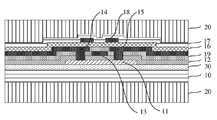
박막 트랜지스터와 이를 제조하는 방법, 디스플레이 패널 및 디스플레이를 장치를 제공한다. 상기 박막 트랜지스터는, 플렉서블 기판(10) 상에 순차적으로 형성된 활성 영역(11), 게이트 절연층(12), 게이트(13), 소스(14)와 드레인(15), 패시베이션층(16) 및 평탄화층(17)을 구비하되, 보호층(18)이 상기 패시베이션층(16) 및 평탄화층(17) 사이에 형성되고 상기 활성 영역(11)과 상기 게이트(13) 바로 상측에 위치한다. 보호층(18)은, 보호층(18)의 수직 영역에서 박막 트랜지스터의 반도체 물질을 보호한다. 따라서, 휨 동작시, 박막 트랜지스터의 물질들 중 일부에 대한 응력이 감소되고, 박막 트랜지스터의 휨동작시, 반도체 물질의 손상을 피하게 됨으로써, 장치의 품질을 개선한다.A thin film transistor, a method of manufacturing the same, a display panel, and a display device. The thin film transistor includes an active region 11, a gate insulating layer 12, a gate 13, a source 14 and a drain 15, a passivation layer 16, and a planarization layer 16 sequentially formed on a flexible substrate 10 A passivation layer 18 is formed between the passivation layer 16 and the planarization layer 17 and is located just above the active region 11 and the gate 13. The passivation layer 18 is formed of a passivation layer 18, The protective layer 18 protects the semiconductor material of the thin film transistor in the vertical region of the protective layer 18. Thus, in the bending operation, the stress on some of the materials of the thin film transistor is reduced, and in the bending operation of the thin film transistor, the damage of the semiconductor material is avoided, thereby improving the quality of the device.
Description
본 발명은 플렉서블 디스플레이 분야에 관한 것으로, 특히, 박막 트랜지스터와 이를 제조하는 방법, 디스플레이 패널 및 디스플레이 장치에 관한 것이다.The present invention relates to a flexible display field, and more particularly, to a thin film transistor, a method of manufacturing the same, a display panel, and a display device.
유기 전계 발광 디스플레이(organic electroluminescence display)로 불리기도 하는 유기 발광 장치, 즉 유기 발광 다이오드(organic light-emitting diode (OLED))는 전고체 상태(all-solid-state) 특성, 양호한 기구적 특성 및 강한 충격 저항성을 가지며, 플라스틱이나 폴리에스테르 막 또는 시트를 기판으로 사용한다. OLED 화면은 얇게 제조 가능하고 심지어 접거나 감을 수 있어, 유연하고 부드러운 화면 디스플레이를 얻을 수 있다.BACKGROUND ART [0002] An organic light emitting diode (OLED), which may also be referred to as an organic electroluminescence display, has an all-solid-state characteristic, a good mechanical characteristic, and a strong Impact resistance, and a plastic or polyester film or sheet is used as a substrate. The OLED screen can be made thin and even folded or rolled, resulting in a flexible, smooth screen display.
디스플레이 기술의 발전으로, 연구 개발 엔지니어들은 접거나 감을 수 있는 플렉서블 디스플레이 장치를 끊임없이 개선하고 있다. 종래의 리지드(rigid) 디스플레이(즉, 유리와 같은 비유연 기판상에 제조된 디스플레이 장치)에 비해, 플렉서블 디스플레이 장치는 더 가벼운 무게, 더 작은 크기, 보다 더 편리한 휴대성, 더 높은 충돌 저항성 및 더 강한 충격 저항성 등의 장점을 많이 가지고 있다. With advances in display technology, R & D engineers are constantly improving flexible display devices that can be folded or rolled. Compared to conventional rigid displays (i.e., display devices made on non-flexible substrates such as glass), flexible display devices have a lower weight, smaller size, more convenient portability, higher crash resistance, and more And strong impact resistance.
그러나, 플렉서블 디스플레이 장치를 구부리면, 층간 영의 계수(Young's modulus) 차이로 인해 다층 구조의 인터페이스에 많은 결함이 생기게 됨으로써, 장치 성능에 영향을 줄 수 있다. 플렉서블 디스플레이 장치에서 박막 트랜지스터는 주요 기능 소자이고, 따라서 이의 성능은 플렉서불 제품의 전체 성능에 중요한 영향을 미친다. 종래 기술에서는, 인접한 구조막 층들을 가능한 한 서로 가깝게 하여 기능층의 손상을 줄이기 위해, 장치 구조의 최적화를 통해 고경도 막층의 두께를 감소시키는 것이 일반적이었다. 그러나, 박막 트랜지스터의 서로 다른 층들의 소재 두께를 감소시키면, 박막 트랜지스터의 성능에 영향을 미치게 되어 최종 제품은 원하는 효과를 거두기 어렵다. However, if the flexible display device is bent, a difference in Young's modulus may cause a large number of defects in the interface of the multi-layer structure, which may affect device performance. In flexible display devices, thin-film transistors are the main functioning device, and therefore its performance has a significant impact on the overall performance of the flexor bulb. In the prior art, it has been common to reduce the thickness of the hard film layer through optimization of the device structure in order to reduce the damage of the functional layer by bringing the adjacent structure film layers as close to each other as possible. However, if the thickness of the material of the different layers of the thin film transistor is reduced, the performance of the thin film transistor is affected, and the final product is difficult to achieve the desired effect.
따라서, 휨 동작시 박막 트랜지스터의 손상을 막는 방법을 제공하는 것이 시급하게 필요하다.Therefore, it is urgently required to provide a method of preventing the damage of the thin film transistor in the bending operation.
본 발명의 목적은, 박막 트랜지스터 장치를 구부리는 동안, 보호층에 의해 덮여있는 박막 트랜지스터내의 반도체 물질을 보호하고, 상기 박막 트랜지스터의 물질의 일부에 대한 응력을 감소시키며, 상기 반도체 물질에 대한 손상을 피하도록 하는, 상기 박막 트랜지스터와 이를 제조하는 방법, 디스플레이 패널 및 디스플레이 장치를 제공하는 것이다.It is an object of the present invention to provide a method of protecting a semiconductor material in a thin film transistor covered by a protective layer while bending the thin film transistor device and reducing stress on a part of the material of the thin film transistor, A thin film transistor, a method of manufacturing the thin film transistor, a display panel, and a display device.
상기 목적을 달성하기 위해, 본 발명은 박막 트랜지스터를 제공한다. 상기 박막 트랜지스터는 플렉서블 기판 상에 순차적으로 형성된, 활성 영역, 게이트 절연층, 게이트, 소스 및 드레인, 패시베이션층 및 평탄화층을 구비하되, 보호층은 상기 패시베이션층과 상기 평탄화층 사이에 제공되고, 상기 보호층은 상기 활성 영역과 상기 게이트 바로 상측에 위치한다.In order to achieve the above object, the present invention provides a thin film transistor. Wherein the thin film transistor has an active region, a gate insulating layer, a gate, a source and a drain, a passivation layer and a planarization layer sequentially formed on a flexible substrate, wherein a protective layer is provided between the passivation layer and the planarization layer, The protective layer is located above the active region and directly above the gate.
또는, 상기 박막 트랜지스터에서, 상기 보호층은 상기 활성 영역과 상기 게이트 바로 상측에 위치하고, 상기 게이트에 수직인 방향으로 상기 게이트를 완전히 덮는다. Alternatively, in the thin film transistor, the protective layer is located above the active region and directly above the gate, and completely covers the gate in a direction perpendicular to the gate.
또는, 상기 박막 트랜지스터에서, 상기 보호층은 유기 물질로 형성된다.Alternatively, in the thin film transistor, the protective layer is formed of an organic material.
또는, 상기 박막 트랜지스터에서, 상기 보호층은 금속으로 형성된다.Alternatively, in the thin film transistor, the protective layer is formed of a metal.
또는, 상기 박막 트랜지스터에서, 상기 보호층은 상기 게이트에 수직인 방향으로 상기 게이트와 상기 드레인 사이의 갭 뿐만 아니라 상기 게이트와 상기 소스 사이의 갭을 덮는다.Alternatively, in the thin film transistor, the protective layer covers a gap between the gate and the source, as well as a gap between the gate and the drain in a direction perpendicular to the gate.
또는, 상기 박막 트랜지스터에서, 상기 보호층의 영 계수(Young's modulus)는 300N/m2 보다 크다.Alternatively, in the thin film transistor, the Young's modulus of the protective layer is greater than 300 N / m 2 .
또는, 상기 박막 트랜지스터는 상부 보호막, 하부 보호막 및 배리어층(barrier layer)을 더 구비하되, 상기 상부 보호막은 상기 평탄화층 상측에 제공되고, 상기 하부 보호막은 상기 플렉서블 기판 하측에 제공되며, 상기 배리어층은 상기 플렉서블 기판과 상기 게이트 절연층 사이에 제공된다.Alternatively, the thin film transistor may further include an upper protective layer, a lower protective layer, and a barrier layer, wherein the upper protective layer is provided on the upper side of the planarization layer, the lower protective layer is provided below the flexible substrate, Is provided between the flexible substrate and the gate insulating layer.
따라서, 본 발명은 또한 상기에서 설명한 박막 트랜지스터를 제조하기 위해, 박막 트랜지스터 제조 방법을 제공한다. 상기 방법은 플렉서블 기판 상에 활성 영역, 게이트 절연층, 게이트, 소스 및 드레인, 그리고 패시베이션층을 순차적으로 형성하는 단계, 상기 패시베이션층 위에 보호층을 형성하는 단계, 및 상기 보호층 위에 평탄화층을 형성하는 단계를 구비하되, 상기 보호층은 상기 활성 영역과 상기 게이트 바로 상측에 위치한다. Therefore, the present invention also provides a method of manufacturing a thin film transistor for manufacturing the thin film transistor described above. The method includes sequentially forming an active region, a gate insulating layer, a gate, a source and a drain, and a passivation layer on a flexible substrate, forming a passivation layer on the passivation layer, and forming a planarization layer on the passivation layer Wherein the protective layer is located directly above the active region and the gate.
따라서, 본 발명은 또한 상기에서 설명한 박막 트랜지스터를 구비하는 디스플레이 패널을 제공한다. Accordingly, the present invention also provides a display panel comprising the above-described thin film transistor.
따라서, 본 발명은 또한 상기에서 설명한 디스플레이 패널을 구비하는 디스플레이 장치를 제공한다. Accordingly, the present invention also provides a display device having the display panel described above.
종래 기술에 비해, 본 발명에 따른 박막 트랜지스터와 이를 제조하는 방법, 디스플레이 패널 및 디스플레이 장치는 다음과 같은 장점을 가진다.The thin film transistor, the method of manufacturing the thin film transistor, the display panel and the display device according to the present invention have the following advantages over the prior art.
1. 보호층이 상기 패시베이션층 및 평탄화층 사이에 형성되고 상기 활성 영역과 상기 게이트 바로 상측에 위치하여, 보호층의 수직 영역에서 박막 트랜지스터의 반도체 물질을 보호한다. 따라서, 휨 동작시, 박막 트랜지스터의 물질들 중 일부에 대한 응력이 감소되고, 박막 트랜지스터의 휨동작시, 반도체 물질의 손상을 피하게 됨으로써, 장치의 품질을 개선한다.1. A protective layer is formed between the passivation layer and the planarization layer and is located above the active region and directly above the gate to protect the semiconductor material of the thin film transistor in the vertical region of the protective layer. Thus, in the bending operation, the stress on some of the materials of the thin film transistor is reduced, and in the bending operation of the thin film transistor, the damage of the semiconductor material is avoided, thereby improving the quality of the device.
2. 보호층이 금속으로 형성될 경우, 보호층은 활성 영역의 일부분을 덮고, 게이트에 대해 수직인 방향으로 게이트와 드레인 사이의 갭과 게이트와 소스 사이의 갭을 완전히 덮는다. 게이트의 물질 역시 양호한 지지 특성을 가지고 있기 때문에, 보호층과 게이트가 중첩되는 상기 구조는 하측의 반도체 물질을 보호할 수 있다. 더욱이, 보호층과 게이트는 상대적으로 매우 작은 영역에서 중첩되므로, 기생 커패시턴스에 의해 발생하는 박막 트랜지스터에 대한 보호층의 의 영향을 감소시킬 수 있다.2. When the protective layer is formed of a metal, the protective layer covers a portion of the active region and completely covers the gap between the gate and the drain and the gap between the gate and the source in a direction perpendicular to the gate. Since the material of the gate also has good support properties, the structure in which the protective layer and the gate overlap can protect the underlying semiconductor material. Moreover, since the protective layer and the gate overlap in a relatively small area, the influence of the protective layer on the thin film transistor caused by the parasitic capacitance can be reduced.
도 1은 본 발명의 일 실시예에 따른 박막 트랜지스터의 개략 구조도이다.
도 2는 본 발명의 일 실시예에 따른 다른 박막 트랜지스터의 개략 구조도이다.1 is a schematic structural view of a thin film transistor according to an embodiment of the present invention.
2 is a schematic structural view of another thin film transistor according to an embodiment of the present invention.
본 발명의 내용을 보다 명확히 쉽게 이해할 수 있도록, 본 발명의 내용을 명세서의 첨부 도면을 참조하여 하기에서 상세하게 설명한다. 본 발명은 특정 실시예에 한정되지 않으며 당업자에게 공지된 일반적인 대체물은 본 발명의 보호 범위에 속함은 자명하다.In order that the contents of the present invention can be more clearly understood, the contents of the present invention will be described in detail below with reference to the accompanying drawings. It is to be understood that the invention is not limited to the specific embodiments, and that the generic alternatives known to those skilled in the art fall within the scope of protection of the present invention.
둘째, 본 발명은 구조도를 이용하여 상세히 설명한다. 본 발명의 예시를 상세히 설명함에 있어, 설명을 용이하게 하기 위해, 도면은 일반 척도에 따라 부분 확대되지 않았으며, 이는 본 발명의 한정으로 구성되어서는 안 된다.Second, the present invention will be described in detail using a structural diagram. In describing the exemplary embodiments of the present invention in detail, for ease of explanation, the drawings are not to scale in accordance with the general scale, and they should not be construed as limiting the present invention.
본 발명의 핵심 개념은, 박막 트랜지스터의 패시베이션층(passivation layer)과 평탄화층 (planarization layer) 사이에 보호층이 형성되고, 상기 보호층은 활성 영역과 게이트 바로 상측에 위치하여, 상기 보호층에 의해 가려지는 수직 영역내의 반도체 물질을 보호하는데 있다. 따라서, 휨 동작시, 박막 트랜지스터의 물질들 중 일부에 대한 응력이 감소되고, 상기 박막 트랜지스터에 대한 휨 동작시, 상기 반도체 물질에 대한 손상을 피하게 됨으로써, 상기 장치의 품질을 개선한다.A key concept of the present invention is that a passivation layer is formed between a passivation layer and a planarization layer of a thin film transistor and the passivation layer is located directly above the active region and the gate, To protect the semiconductor material in the vertical region covered. Thus, during the bending operation, the stress on some of the materials of the thin film transistor is reduced, and during the bending operation for the thin film transistor, the damage to the semiconductor material is avoided, thereby improving the quality of the device.
실시예 1Example 1
도 1은 본 발명의 일 실시예에 따른 박막 트랜지스터를 도시하는 개략적 구조도이다. 도 1 에 도시된 바와 같이, 본 실시예에 따른 박막 트랜지스터는, 플렉서블 기판(10) 상에 순차적으로 형성된, 활성 영역(11), 게이트 절연층(12), 게이트(13), 소스(14)와 드레인(15), 패시베이션층(16) 및 평탄화층(17)을 구비하되, 보호층(18)이 상기 패시베이션층(16) 및 평탄화층(17) 사이에 형성되고, 상기 보호층(18)은 상기 활성 영역(11)과 상기 게이트(13) 바로 상측에 위치한다.1 is a schematic structural view showing a thin film transistor according to an embodiment of the present invention. 1, the thin film transistor according to the present embodiment includes an
도 1에서 알 수 있듯이, 보호층(18)은 활성 영역(11)과 게이트(13) 바로 상측에 위치하여, 게이트(13)에 수직인 방향으로 게이트(13)를 완전히 덮는다. 수직 방향으로 게이트(13)를 완전히 덮을 뿐만 아니라, 보호층(18)은 적어도 (바람직하게는, 완전히) 게이트(13)와 드레인(15) 사이의 갭(gap)과 게이트(13)와 소스(14) 사이의 갭에 해당하는 영역도 덮는 것이 바람직하다. 보호층(18)의 물질은 유기 물질이거나 금속이고, 또는 당업자에게 알려진 다른 물질이 될 수도 있다. 보호층(18)은, 보호층(18)의 수직 영역에서 박막 트랜지스터의 반도체 물질을 보호한다. 따라서, 휨 동작시, 박막 트랜지스터의 물질들 중 일부에 대한 응력이 감소되고, 박막 트랜지스터 장치를 구부리는 동안, 반도체 물질의 손상을 피하게 됨으로써, 장치의 품질을 개선한다.1, the
보호층(18)의 영 계수(Young's modulus)는 300 N/m2보다 큰 값, 이를테면, 350 N/m2, 400 N/m2, 450 N/m2, 또는 500 N/m2임이 바람직하다. 따라서, 휨 동작시 보호층(18) 하측에 있는 박막 트랜지스터의 일부에 대한 응력을 효과적으로 감소시킬 수 있다.The Young's modulus of the
보호층(18)이 금속으로 형성될 경우, 금속 보호층과 게이트(13) 사이에 기생 커패시턴스(parasite capacitance)가 발생되어, 박막 트랜지스터의 성능에 영향을 줄 수 있다. 따라서, 박막 트랜지스터에 대한 다른 구조적 해결 방법에서는, 금속 보호층과 게이트(13) 사이의 중첩 영역을 모든 방법에 의해 감소시킬 수 있다. 도 2에 도시된 바와 같이, 보호층(18)은 금속으로 형성된다. 보호층(18)은 게이트(13)에 수직 방향에 있는 활성 영역(11)의 일부분을 덮고, 게이트(13)와 드레인(15) 사이의 갭과 게이트(13)와 소스(14) 사이의 갭을 완전히 덮는다. 게이트(13) 역시 금속으로 형성되기 때문에, 게이트(13) 자체는 양호한 지지 특성을 가질 수 있다. 따라서, 보호층(18)은 게이트(13)와 드레인(15) 사이의 갭과 게이트(13)와 소스(14) 사이의 갭을 보호하는데 주로 이용될 수 있다. 도 2에 도시된 구조에서, 보호층(18)과 게이트(13)는 수직 방향으로 매우 작은 중첩 영역을 가질 수 있다. 보호층(18)과 게이트(13)(둘 다 금속으로 형성된다)가 중첩되는 상기 구조는 하측의 반도체 물질을 보호할 수 있다. 더욱이, 보호층(18)과 게이트(13)는 상대적으로 매우 작은 영역에서 중첩되므로, 기생 커패시턴스가 수용가능한 범위내에서 조절될 수 있다. 예를 들면, 기생 커패시턴스는 미리 설정된 임계값 보다 작게 조절됨으로써, 박막 트랜지스터에 대한 기생 커패시턴스의 영향을 저하시킨다.When the
상기 박막 트랜지스터는, 상부 보호막(20), 하부 보호막(20) 및 배리어층(barrier film)(30)을 더 구비한다. 상부 보호막(20)은 평탄화층(17) 상측에 제공되고, 하부 보호막(20)은 플렉서블 기판(10) 하측에 제공된다. 물과 산소 분자에 대한 절연을 위해, 배리어층(30)은 플렉서블 기판(10)과 게이트 절연층(12) 사이에 제공된다. 또한, 도 1과 도 2에 도시된 구조에서 층간 절연층(19)이 더 형성되고, 층간 절연층(19)은 게이트(13)를 덮는다.The thin film transistor further includes an upper
종래의 박막 트랜지스터를 바탕으로, 본 발명에 따른 박막 트랜지스터는 패시베이션층과 평탄화층 사이에 보호층이 형성되어 하측의 반도체 물질을 보호하는 것으로 이해할 수 있다. 따라서, 상기 박막 트랜지스터의 구성요소는 간단히 설명한다.Based on the conventional thin film transistor, it can be understood that the thin film transistor according to the present invention protects the underlying semiconductor material by forming a passivation layer between the passivation layer and the planarization layer. Therefore, the components of the thin film transistor will be briefly described.
실시예 2Example 2
본 발명은 실시예 1에서 설명한 박막 트랜지스터를 제조하는 방법을 제공한다. 상기 방법은, 플렉서블 기판(10) 상에 활성 영역(11), 게이트 절연층(12), 게이트(13), 소스(14)와 드레인(15) 및 패시베이션층(16)을 순차적으로 형성하는 단계를 구비하되, 보호층(18)은 상기 패시베이션층(16) 상에 형성되고, 평탄화층(17)은 상기 보호층(18) 상에 형성되며, 상기 보호층(18)은 상기 활성 영역(11)과 상기 게이트(13) 바로 상측에 위치한다. 최종적으로, 도 1 및 도 2에 도시된 구조가 형성된다.The present invention provides a method of manufacturing the thin film transistor described in the first embodiment. The method comprises sequentially forming an
보호층(18)은, 보호층(18)의 수직 영역에서 박막 트랜지스터의 반도체 물질을 보호한다. 따라서, 휨 동작시, 박막 트랜지스터의 물질들 중 일부에 대한 응력이 감소되고, 박막 트랜지스터의 휨동작시, 반도체 물질의 손상을 피하게 됨으로써, 장치의 품질을 개선한다.The
보호층(18)은 도 1과 도 2에 각각 도시된 서로 다른 보호층 물질에 따라, 실시예 1에서 설명한 서로 다른 구조들로 형성된다.The
실시예 3Example 3
본 실시예는, 실시예 1에서 설명한 박막 트랜지스터를 구비하는 디스플레이 패널을 제공한다.This embodiment provides a display panel comprising the thin film transistor described in the first embodiment.
본 실시예의 디스플레이 패널은 실시예 1에서 설명한 박막 트랜지스터를 가진다. 따라서, 보호층은 상기 박막 트랜지스터의 패시베이션층과 평탄화층 사이에 형성되고, 활성 영역과 게이트 바로 상측에 위치하여, 보호층에 의해 덮여지는 수직 영역내의 반도체 물질을 보호한다. 따라서, 휨 동작시, 박막 트랜지스터의 물질들 중 일부에 대한 응력이 감소되고, 박막 트랜지스터의 휨동작시, 반도체 물질의 손상을 피하게 됨으로써, 장치의 품질을 개선한다. 보호층이 금속으로 형성될 경우, 보호층은 활성 영역의 일부분을 덮고, 게이트에 대해 수직인 방향으로 게이트와 드레인 사이의 갭과 게이트와 소스 사이의 갭을 완전히 덮는다. 게이트의 물질 역시 양호한 지지 특성을 가지고 있기 때문에, 보호층과 게이트가 중첩되는 상기 구조는 하측의 반도체 물질을 보호할 수 있다. 더욱이, 보호층과 게이트는 상대적으로 매우 작은 영역에서 중첩되므로, 박막 트랜지스터에 대한 기생 커패시턴스의 영향을 감소시킬 수 있다.The display panel of this embodiment has the thin film transistor described in the first embodiment. Thus, a protective layer is formed between the passivation layer and the planarization layer of the thin film transistor, and is located directly above the active region and the gate to protect the semiconductor material in the vertical region covered by the protective layer. Thus, in the bending operation, the stress on some of the materials of the thin film transistor is reduced, and in the bending operation of the thin film transistor, the damage of the semiconductor material is avoided, thereby improving the quality of the device. When the protective layer is formed of a metal, the protective layer covers a portion of the active region and completely covers the gap between the gate and the drain and the gap between the gate and the source in a direction perpendicular to the gate. Since the material of the gate also has good support properties, the structure in which the protective layer and the gate overlap can protect the underlying semiconductor material. Furthermore, since the protective layer and the gate overlap in a relatively small region, the influence of the parasitic capacitance on the thin film transistor can be reduced.
실시예 4 Example 4
본 실시예는, 실시예 3에서 설명한 디스플레이 패널을 구비하는 디스플레이장치를 제공한다.The present embodiment provides a display device having the display panel described in the third embodiment.
본 실시예의 상기 디스플레이 장치는 실시예 3에서 설명한 디스플레이 패널을 가진다. 따라서, 보호층은 상기 박막 트랜지스터의 패시베이션층과 평탄화층 사이에 형성되고, 활성 영역과 게이트 바로 상측에 위치하여, 보호층에 의해 덮여지는 수직 영역내의 반도체 물질을 보호한다. 따라서, 휨 동작시, 박막 트랜지스터의 물질들 중 일부에 대한 응력이 감소되고, 박막 트랜지스터의 휨동작시, 반도체 물질의 손상을 피하게 됨으로써, 장치의 품질을 개선한다. 보호층이 금속으로 형성될 경우, 보호층은 활성 영역의 일부분을 덮고, 게이트에 대해 수직인 방향으로 게이트와 드레인 사이의 갭과 게이트와 소스 사이의 갭을 완전히 덮는다. 게이트의 물질 역시 양호한 지지 특성을 가지고 있기 때문에, 보호층과 게이트가 중첩되는 상기 구조는 하측의 반도체 물질을 보호할 수 있다. 더욱이, 보호층과 게이트는 상대적으로 매우 작은 영역에서 중첩되므로, 기생 커패시턴스에 의해 발생하는 박막 트랜지스터에 대한 보호층의 영향을 감소시킬 수 있다.The display device of this embodiment has the display panel described in the third embodiment. Thus, a protective layer is formed between the passivation layer and the planarization layer of the thin film transistor, and is located directly above the active region and the gate to protect the semiconductor material in the vertical region covered by the protective layer. Thus, in the bending operation, the stress on some of the materials of the thin film transistor is reduced, and in the bending operation of the thin film transistor, the damage of the semiconductor material is avoided, thereby improving the quality of the device. When the protective layer is formed of a metal, the protective layer covers a portion of the active region and completely covers the gap between the gate and the drain and the gap between the gate and the source in a direction perpendicular to the gate. Since the material of the gate also has good support properties, the structure in which the protective layer and the gate overlap can protect the underlying semiconductor material. Furthermore, since the protective layer and the gate overlap in a relatively small area, the influence of the protective layer on the thin film transistor caused by the parasitic capacitance can be reduced.
정리하면, 본 발명에 따른 박막 트랜지스터와 이의 제조방법, 디스플레이 패널 및 디스플레이 장치에 있어서, 보호층은 상기 박막 트랜지스터의 패시베이션층과 평탄화층 사이에 형성되고, 활성 영역과 게이트 바로 상측에 위치하여, 보호층에 의해 덮여지는 수직 영역내의 반도체 물질을 보호한다. 따라서, 휨 동작시, 박막 트랜지스터의 물질들 중 일부에 대한 응력이 감소되고, 박막 트랜지스터의 휨동작시, 반도체 물질의 손상을 피하게 됨으로써, 장치의 품질을 개선한다. 보호층이 금속으로 형성될 경우, 보호층은 활성 영역의 일부분을 덮고, 게이트에 대해 수직인 방향으로 게이트와 드레인 사이의 갭과 게이트와 소스 사이의 갭을 완전히 덮는다. 게이트의 물질 역시 양호한 지지 특성을 가지고 있기 때문에, 보호층과 게이트가 중첩되는 상기 구조는 하측의 반도체 물질을 보호할 수 있다. 더욱이, 보호층과 게이트는 상대적으로 매우 작은 영역에서 중첩되므로, 박막 트랜지스터에 대한 기생 커패시턴스의 영향을 감소시킬 수 있다.In summary, in the thin film transistor, the method of manufacturing the same, the method of manufacturing the same, the display panel and the display device, the protective layer is formed between the passivation layer and the planarization layer of the thin film transistor, Thereby protecting the semiconductor material in the vertical region covered by the layer. Thus, in the bending operation, the stress on some of the materials of the thin film transistor is reduced, and in the bending operation of the thin film transistor, the damage of the semiconductor material is avoided, thereby improving the quality of the device. When the protective layer is formed of a metal, the protective layer covers a portion of the active region and completely covers the gap between the gate and the drain and the gap between the gate and the source in a direction perpendicular to the gate. Since the material of the gate also has good support properties, the structure in which the protective layer and the gate overlap can protect the underlying semiconductor material. Furthermore, since the protective layer and the gate overlap in a relatively small region, the influence of the parasitic capacitance on the thin film transistor can be reduced.
상기에서는 본 발명의 바람직한 실시예들을 설명했을 뿐, 본 발명의 범위를 한정하지는 않는다. 상기 개시에 따른 당업자의 어떠한 변경이나 수정도 청구범위의 보호 범위에 모두 포함된다.The foregoing has described preferred embodiments of the present invention and is not intended to limit the scope of the present invention. Any modifications or alterations by those skilled in the art in light of the foregoing disclosure are intended to be included within the scope of the claims.
10: 플렉서블 기판 11: 활성 영역
12: 게이트 절연층 13: 게이트
14: 소스 15: 드레인
16: 패시베이션층 17: 평탄화층
18: 보호층 19: 층간 절연층
20: 상부 보호막 20: 하부 보호막
30: 배리어층10: flexible substrate 11: active region
12: gate insulating layer 13: gate
14: source 15: drain
16: passivation layer 17: planarization layer
18: protective layer 19: interlayer insulating layer
20: upper protective film 20: lower protective film
30: barrier layer
Claims (10)
플렉서블 기판 상에 순차적으로 형성된, 활성 영역, 게이트 절연층, 게이트, 소스 및 드레인, 패시베이션층 및 평탄화층을 구비하되, 보호층은 상기 패시베이션층과 상기 평탄화층 사이에 제공되고, 상기 보호층은 상기 활성 영역과 상기 게이트 바로 상측에 위치함을 특징으로 하는, 박막 트랜지스터.
In the thin film transistor,
A semiconductor device, comprising: an active region, a gate insulating layer, a gate, a source and a drain, a passivation layer and a planarization layer sequentially formed on a flexible substrate, wherein a protective layer is provided between the passivation layer and the planarization layer, The active region and the gate immediately above the gate.
상기 보호층은 상기 게이트에 수직인 방향으로 상기 게이트를 완전히 덮음을 특징으로 하는, 박막 트랜지스터.
The method according to claim 1,
Wherein the protective layer completely covers the gate in a direction perpendicular to the gate.
상기 보호층은 유기 물질로 형성됨을 특징으로 하는, 박막 트랜지스터.
The method according to claim 1,
Wherein the protective layer is formed of an organic material.
The thin film transistor of claim 1, wherein the protective layer is formed of a metal.
상기 보호층은, 상기 게이트에 수직인 방향으로 상기 게이트와 상기 드레인 사이의 갭 뿐만 아니라 상기 게이트와 상기 소스 사이의 갭을 덮음을 특징으로 하는, 박막 트랜지스터.
5. The method of claim 4,
Wherein the protective layer covers a gap between the gate and the source as well as a gap between the gate and the drain in a direction perpendicular to the gate.
상기 보호층의 영 계수(Young's modulus)는 300N/m2 보다 큼을 특징으로 하는, 박막 트랜지스터.
The method according to claim 1,
Wherein a Young's modulus of the protective layer is greater than 300 N / m 2 .
상부 보호막, 하부 보호막 및 배리어층(barrier layer)을 더 구비하되,
상기 상부 보호막은 상기 평탄화층 상측에 제공되고, 상기 하부 보호막은 상기 플렉서블 기판 하측에 제공되며, 상기 배리어층은 상기 플렉서블 기판과 상기 게이트 절연층 사이에 제공됨을 특징으로 하는, 박막 트랜지스터.
7. The method according to any one of claims 1 to 6,
Further comprising a top protective layer, a bottom protective layer, and a barrier layer,
Wherein the upper protective film is provided on the planarizing layer, the lower protective film is provided on the lower side of the flexible substrate, and the barrier layer is provided between the flexible substrate and the gate insulating layer.
플렉서블 기판 상에 활성 영역, 게이트 절연층, 게이트, 소스 및 드레인, 그리고 패시베이션층을 순차적으로 형성하는 단계;
상기 패시베이션층 위에 보호층을 형성하는 단계; 및
상기 보호층 위에 평탄화층을 형성하는 단계를 구비하되,
상기 보호층은 상기 활성 영역과 상기 게이트 바로 상측에 위치함을 특징으로 하는, 방법.
A method of manufacturing a thin film transistor as set forth in any one of claims 1 to 7,
Sequentially forming an active region, a gate insulating layer, a gate, a source and a drain, and a passivation layer on a flexible substrate;
Forming a passivation layer over the passivation layer; And
And forming a planarization layer on the protective layer,
Wherein the protective layer is located on the active region and directly above the gate.
A display panel comprising the thin film transistor described in any one of claims 1 to 7.
Applications Claiming Priority (3)
| Application Number | Priority Date | Filing Date | Title |
|---|---|---|---|
| CN201610111984.XA CN107134496B (en) | 2016-02-29 | 2016-02-29 | Thin film transistor and method for manufacturing the same, display panel and display device |
| CN201610111984.X | 2016-02-29 | ||
| PCT/CN2017/075001 WO2017148348A1 (en) | 2016-02-29 | 2017-02-27 | Thin film transistor and manufacturing method therefor, display panel and display apparatus |
Publications (2)
| Publication Number | Publication Date |
|---|---|
| KR20180098363A true KR20180098363A (en) | 2018-09-03 |
| KR102155434B1 KR102155434B1 (en) | 2020-09-11 |
Family
ID=59721172
Family Applications (1)
| Application Number | Title | Priority Date | Filing Date |
|---|---|---|---|
| KR1020187021458A Active KR102155434B1 (en) | 2016-02-29 | 2017-02-27 | Thin film transistor and manufacturing method therefor, display panel and display device |
Country Status (7)
| Country | Link |
|---|---|
| US (1) | US10424667B2 (en) |
| EP (1) | EP3425677B1 (en) |
| JP (1) | JP6749400B2 (en) |
| KR (1) | KR102155434B1 (en) |
| CN (1) | CN107134496B (en) |
| TW (1) | TWI673866B (en) |
| WO (1) | WO2017148348A1 (en) |
Families Citing this family (4)
| Publication number | Priority date | Publication date | Assignee | Title |
|---|---|---|---|---|
| CN108091612B (en) * | 2017-12-07 | 2020-11-24 | 深圳市华星光电半导体显示技术有限公司 | Array substrate and preparation method thereof |
| CN108054291B (en) * | 2017-12-28 | 2019-10-01 | 上海天马有机发光显示技术有限公司 | A kind of flexible display panel and its preparation method, flexible display device |
| CN109887956B (en) * | 2019-01-25 | 2021-04-27 | 武汉华星光电半导体显示技术有限公司 | Flexible array substrate of organic light emitting diode |
| TW202032226A (en) * | 2020-01-14 | 2020-09-01 | 友達光電股份有限公司 | Structure of flexible circuits |
Citations (7)
| Publication number | Priority date | Publication date | Assignee | Title |
|---|---|---|---|---|
| KR20040061656A (en) * | 2002-12-31 | 2004-07-07 | 삼성전자주식회사 | Thin film transistor with protective cap over flexible substrate and electronic device using the same and manufacturing method thereof |
| KR20080027185A (en) * | 2006-09-22 | 2008-03-26 | 가부시키가이샤 한도오따이 에네루기 켄큐쇼 | Semiconductor device |
| EP2071627A2 (en) * | 2007-12-03 | 2009-06-17 | Semiconductor Energy Laboratory Co., Ltd. | Semiconductor device |
| JP2011171287A (en) * | 2010-01-20 | 2011-09-01 | Semiconductor Energy Lab Co Ltd | Flexible light-emitting device, electronic equipment, and manufacturing method for flexible light-emitting device |
| KR20130087915A (en) * | 2012-01-30 | 2013-08-07 | 서울대학교산학협력단 | Thin film transistor and the manufacturing method thereof |
| KR20150026709A (en) * | 2013-08-30 | 2015-03-11 | 엘지디스플레이 주식회사 | Plastic organic electroluminescent device and method for fabricating the same |
| US20150301195A1 (en) * | 2009-06-17 | 2015-10-22 | The Regents Of The University Of Michigan | Photodiode and other sensor structures in flat-panel x-ray imagers and method for improving topological uniformity of the photodiode and other sensor structures in flat-panel x-ray imagers based on thin-film electronics |
Family Cites Families (22)
| Publication number | Priority date | Publication date | Assignee | Title |
|---|---|---|---|---|
| US5828084A (en) * | 1995-03-27 | 1998-10-27 | Sony Corporation | High performance poly-SiGe thin film transistor |
| JP5350616B2 (en) | 2006-09-22 | 2013-11-27 | 株式会社半導体エネルギー研究所 | Semiconductor device |
| KR101363835B1 (en) * | 2007-02-05 | 2014-02-17 | 엘지디스플레이 주식회사 | Display device and method of manufacturing the same |
| US7973316B2 (en) * | 2007-03-26 | 2011-07-05 | Semiconductor Energy Laboratory Co., Ltd. | Semiconductor device and method for manufacturing semiconductor device |
| KR101298234B1 (en) * | 2010-03-19 | 2013-08-22 | 엘지디스플레이 주식회사 | In-plane switching mode liquid crystal display device having touch sensing function and method of fabricating the same |
| KR101829313B1 (en) * | 2011-11-03 | 2018-02-20 | 삼성디스플레이 주식회사 | Flexible display device |
| KR101484022B1 (en) * | 2012-05-31 | 2015-01-19 | 엘지디스플레이 주식회사 | Array Substrate for Liquid Crystal Display and Method for Fabricating The Same |
| CN103681869A (en) * | 2012-08-31 | 2014-03-26 | 群康科技(深圳)有限公司 | Thin film transistor substrate, manufacturing method for thin film transistor substrate, and display |
| US8999771B2 (en) * | 2012-09-28 | 2015-04-07 | Apple Inc. | Protection layer for halftone process of third metal |
| KR20140060776A (en) * | 2012-11-12 | 2014-05-21 | 삼성디스플레이 주식회사 | Flexible display device and manufacturing method of the same |
| KR20140063303A (en) * | 2012-11-16 | 2014-05-27 | 삼성디스플레이 주식회사 | Method of manufacturing a flexible display apparatus |
| KR102206412B1 (en) | 2012-12-27 | 2021-01-22 | 엘지디스플레이 주식회사 | Thin film transistor, method for manufacturing the same and display device comprising the same |
| KR102076666B1 (en) * | 2013-04-11 | 2020-02-12 | 엘지디스플레이 주식회사 | Flexible display panel |
| US9876064B2 (en) * | 2013-08-30 | 2018-01-23 | Lg Display Co., Ltd. | Flexible organic electroluminescent device and method for fabricating the same |
| CN203503661U (en) * | 2013-09-24 | 2014-03-26 | 京东方科技集团股份有限公司 | Flexible display substrate and flexible display device |
| CN103500756A (en) * | 2013-10-22 | 2014-01-08 | 深圳市华星光电技术有限公司 | Organic light-emitting device and manufacturing method thereof |
| CN103545320B (en) * | 2013-11-11 | 2015-11-25 | 京东方科技集团股份有限公司 | Display base plate and the flexible display apparatus containing this display base plate |
| KR102107008B1 (en) * | 2013-12-16 | 2020-05-29 | 삼성디스플레이 주식회사 | Organic Light Emitting Display device and Fabrication Method for the same |
| CN104282696B (en) * | 2014-10-22 | 2018-07-13 | 京东方科技集团股份有限公司 | A kind of array substrate and preparation method thereof, display device |
| CN104332478A (en) * | 2014-11-17 | 2015-02-04 | 京东方科技集团股份有限公司 | Array substrate and manufacturing method as well as display device |
| CN104600081A (en) * | 2014-12-31 | 2015-05-06 | 京东方科技集团股份有限公司 | Array substrate and preparation method thereof, display panel and display device |
| CN104795403B (en) * | 2015-04-16 | 2016-08-31 | 京东方科技集团股份有限公司 | A kind of flexible base board and preparation method thereof, display device |
-
2016
- 2016-02-29 CN CN201610111984.XA patent/CN107134496B/en active Active
-
2017
- 2017-02-24 TW TW106106398A patent/TWI673866B/en active
- 2017-02-27 EP EP17759199.7A patent/EP3425677B1/en active Active
- 2017-02-27 US US16/066,796 patent/US10424667B2/en active Active
- 2017-02-27 JP JP2018533945A patent/JP6749400B2/en active Active
- 2017-02-27 KR KR1020187021458A patent/KR102155434B1/en active Active
- 2017-02-27 WO PCT/CN2017/075001 patent/WO2017148348A1/en not_active Ceased
Patent Citations (8)
| Publication number | Priority date | Publication date | Assignee | Title |
|---|---|---|---|---|
| KR20040061656A (en) * | 2002-12-31 | 2004-07-07 | 삼성전자주식회사 | Thin film transistor with protective cap over flexible substrate and electronic device using the same and manufacturing method thereof |
| KR20080027185A (en) * | 2006-09-22 | 2008-03-26 | 가부시키가이샤 한도오따이 에네루기 켄큐쇼 | Semiconductor device |
| US20080073647A1 (en) * | 2006-09-22 | 2008-03-27 | Semiconductor Energy Laboratory Co., Ltd. | Semiconductor device |
| EP2071627A2 (en) * | 2007-12-03 | 2009-06-17 | Semiconductor Energy Laboratory Co., Ltd. | Semiconductor device |
| US20150301195A1 (en) * | 2009-06-17 | 2015-10-22 | The Regents Of The University Of Michigan | Photodiode and other sensor structures in flat-panel x-ray imagers and method for improving topological uniformity of the photodiode and other sensor structures in flat-panel x-ray imagers based on thin-film electronics |
| JP2011171287A (en) * | 2010-01-20 | 2011-09-01 | Semiconductor Energy Lab Co Ltd | Flexible light-emitting device, electronic equipment, and manufacturing method for flexible light-emitting device |
| KR20130087915A (en) * | 2012-01-30 | 2013-08-07 | 서울대학교산학협력단 | Thin film transistor and the manufacturing method thereof |
| KR20150026709A (en) * | 2013-08-30 | 2015-03-11 | 엘지디스플레이 주식회사 | Plastic organic electroluminescent device and method for fabricating the same |
Also Published As
| Publication number | Publication date |
|---|---|
| CN107134496A (en) | 2017-09-05 |
| US20190027610A1 (en) | 2019-01-24 |
| JP2019505838A (en) | 2019-02-28 |
| TWI673866B (en) | 2019-10-01 |
| TW201742244A (en) | 2017-12-01 |
| EP3425677A4 (en) | 2019-03-13 |
| EP3425677A1 (en) | 2019-01-09 |
| US10424667B2 (en) | 2019-09-24 |
| CN107134496B (en) | 2019-05-31 |
| WO2017148348A1 (en) | 2017-09-08 |
| EP3425677B1 (en) | 2021-03-31 |
| KR102155434B1 (en) | 2020-09-11 |
| JP6749400B2 (en) | 2020-09-02 |
Similar Documents
| Publication | Publication Date | Title |
|---|---|---|
| KR102890367B1 (en) | Display apparatus and method of manufacturing the same | |
| KR102653423B1 (en) | display device | |
| KR102329978B1 (en) | Flexible organic light emitting diode display device | |
| KR102424597B1 (en) | flexible organic light emitting diode display device and method of fabricating the same | |
| KR102668184B1 (en) | Display device | |
| US10090326B2 (en) | Flexible display substrate and a manufacturing method thereof, as well as a flexible display device | |
| JP7085352B2 (en) | Display device | |
| US9553135B2 (en) | Flexible display substrate and method for manufacturing the same | |
| US9287335B2 (en) | Organic light-emitting diode (OLED) display and method of manufacturing the same | |
| WO2018161525A1 (en) | Flexible display panel and manufacturing method, and flexible display apparatus | |
| KR20180032719A (en) | Display device | |
| KR20160141135A (en) | flexible organic light emitting diode display device | |
| US9768411B2 (en) | Organic light emitting display apparatus and manufacturing method thereof | |
| KR20160145898A (en) | Flexible display apparatus and manufacturing method thereof | |
| US10180742B2 (en) | Display panel, method for fabricating the same, and display apparatus | |
| KR20180098363A (en) | Thin film transistor, manufacturing method therefor, display panel and display device | |
| KR20190066648A (en) | Display device and manufacturing method thereof | |
| US9905622B2 (en) | Organic electroluminescent device and manufacturing method thereof, each having a display apparatus | |
| US20180337365A1 (en) | Display device | |
| KR20160032791A (en) | Flexible display apparatus and manufacturing method thereof | |
| CN108122927B (en) | Thin film transistor, manufacturing method thereof, display panel and display device | |
| KR102541451B1 (en) | Display apparatus and manufacturing method thereof | |
| KR20260011657A (en) | Display device | |
| KR102405124B1 (en) | Organic light-emitting display apparatus and manufacturing the same | |
| KR102014169B1 (en) | Organic light emitting display apparatus and method of manufacturing the same |
Legal Events
| Date | Code | Title | Description |
|---|---|---|---|
| A201 | Request for examination | ||
| PA0105 | International application |
St.27 status event code: A-0-1-A10-A15-nap-PA0105 |
|
| PA0201 | Request for examination |
St.27 status event code: A-1-2-D10-D11-exm-PA0201 |
|
| PG1501 | Laying open of application |
St.27 status event code: A-1-1-Q10-Q12-nap-PG1501 |
|
| D13-X000 | Search requested |
St.27 status event code: A-1-2-D10-D13-srh-X000 |
|
| D14-X000 | Search report completed |
St.27 status event code: A-1-2-D10-D14-srh-X000 |
|
| R18-X000 | Changes to party contact information recorded |
St.27 status event code: A-3-3-R10-R18-oth-X000 |
|
| E902 | Notification of reason for refusal | ||
| PE0902 | Notice of grounds for rejection |
St.27 status event code: A-1-2-D10-D21-exm-PE0902 |
|
| E13-X000 | Pre-grant limitation requested |
St.27 status event code: A-2-3-E10-E13-lim-X000 |
|
| P11-X000 | Amendment of application requested |
St.27 status event code: A-2-2-P10-P11-nap-X000 |
|
| P13-X000 | Application amended |
St.27 status event code: A-2-2-P10-P13-nap-X000 |
|
| E902 | Notification of reason for refusal | ||
| PE0902 | Notice of grounds for rejection |
St.27 status event code: A-1-2-D10-D21-exm-PE0902 |
|
| P11-X000 | Amendment of application requested |
St.27 status event code: A-2-2-P10-P11-nap-X000 |
|
| P13-X000 | Application amended |
St.27 status event code: A-2-2-P10-P13-nap-X000 |
|
| E701 | Decision to grant or registration of patent right | ||
| PE0701 | Decision of registration |
St.27 status event code: A-1-2-D10-D22-exm-PE0701 |
|
| GRNT | Written decision to grant | ||
| PR0701 | Registration of establishment |
St.27 status event code: A-2-4-F10-F11-exm-PR0701 |
|
| PR1002 | Payment of registration fee |
St.27 status event code: A-2-2-U10-U12-oth-PR1002 Fee payment year number: 1 |
|
| PG1601 | Publication of registration |
St.27 status event code: A-4-4-Q10-Q13-nap-PG1601 |
|
| P22-X000 | Classification modified |
St.27 status event code: A-4-4-P10-P22-nap-X000 |
|
| P22-X000 | Classification modified |
St.27 status event code: A-4-4-P10-P22-nap-X000 |
|
| PR1001 | Payment of annual fee |
St.27 status event code: A-4-4-U10-U11-oth-PR1001 Fee payment year number: 4 |
|
| PR1001 | Payment of annual fee |
St.27 status event code: A-4-4-U10-U11-oth-PR1001 Fee payment year number: 5 |
|
| P22-X000 | Classification modified |
St.27 status event code: A-4-4-P10-P22-nap-X000 |
|
| PR1001 | Payment of annual fee |
St.27 status event code: A-4-4-U10-U11-oth-PR1001 Fee payment year number: 6 |
|
| U11 | Full renewal or maintenance fee paid |
Free format text: ST27 STATUS EVENT CODE: A-4-4-U10-U11-OTH-PR1001 (AS PROVIDED BY THE NATIONAL OFFICE) Year of fee payment: 6 |