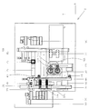
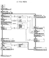
KR20110013440A - 복수의 기판을 처리하는 장치 및 방법 - Google Patents
복수의 기판을 처리하는 장치 및 방법 Download PDFInfo
- Publication number
- KR20110013440A KR20110013440A KR1020107027093A KR20107027093A KR20110013440A KR 20110013440 A KR20110013440 A KR 20110013440A KR 1020107027093 A KR1020107027093 A KR 1020107027093A KR 20107027093 A KR20107027093 A KR 20107027093A KR 20110013440 A KR20110013440 A KR 20110013440A
- Authority
- KR
- South Korea
- Prior art keywords
- substrate
- cutting
- station
- substrates
- loading
- Prior art date
- Legal status (The legal status is an assumption and is not a legal conclusion. Google has not performed a legal analysis and makes no representation as to the accuracy of the status listed.)
- Withdrawn
Links
Images

Classifications
-
- B—PERFORMING OPERATIONS; TRANSPORTING
- B28—WORKING CEMENT, CLAY, OR STONE
- B28D—WORKING STONE OR STONE-LIKE MATERIALS
- B28D5/00—Fine working of gems, jewels, crystals, e.g. of semiconductor material; apparatus or devices therefor
- B28D5/0058—Accessories specially adapted for use with machines for fine working of gems, jewels, crystals, e.g. of semiconductor material
-
- H—ELECTRICITY
- H01—ELECTRIC ELEMENTS
- H01L—SEMICONDUCTOR DEVICES NOT COVERED BY CLASS H10
- H01L21/00—Processes or apparatus adapted for the manufacture or treatment of semiconductor or solid state devices or of parts thereof
- H01L21/70—Manufacture or treatment of devices consisting of a plurality of solid state components formed in or on a common substrate or of parts thereof; Manufacture of integrated circuit devices or of parts thereof
- H01L21/77—Manufacture or treatment of devices consisting of a plurality of solid state components or integrated circuits formed in, or on, a common substrate
- H01L21/78—Manufacture or treatment of devices consisting of a plurality of solid state components or integrated circuits formed in, or on, a common substrate with subsequent division of the substrate into plural individual devices
-
- H10P54/00—
Landscapes
- Engineering & Computer Science (AREA)
- Mechanical Engineering (AREA)
- Physics & Mathematics (AREA)
- Condensed Matter Physics & Semiconductors (AREA)
- General Physics & Mathematics (AREA)
- Manufacturing & Machinery (AREA)
- Computer Hardware Design (AREA)
- Microelectronics & Electronic Packaging (AREA)
- Power Engineering (AREA)
- Dicing (AREA)
- Laser Beam Processing (AREA)
Applications Claiming Priority (2)
| Application Number | Priority Date | Filing Date | Title |
|---|---|---|---|
| SG200803452-2A SG142402A1 (en) | 2008-05-02 | 2008-05-02 | Apparatus and method for multiple substrate processing |
| SG200803452-2 | 2008-05-02 |
Publications (1)
| Publication Number | Publication Date |
|---|---|
| KR20110013440A true KR20110013440A (ko) | 2011-02-09 |
Family
ID=41255265
Family Applications (1)
| Application Number | Title | Priority Date | Filing Date |
|---|---|---|---|
| KR1020107027093A Withdrawn KR20110013440A (ko) | 2008-05-02 | 2009-05-04 | 복수의 기판을 처리하는 장치 및 방법 |
Country Status (6)
| Country | Link |
|---|---|
| US (1) | US20110036339A1 (enExample) |
| JP (1) | JP5420640B2 (enExample) |
| KR (1) | KR20110013440A (enExample) |
| CN (1) | CN102046344A (enExample) |
| SG (1) | SG142402A1 (enExample) |
| WO (1) | WO2009134212A1 (enExample) |
Cited By (2)
| Publication number | Priority date | Publication date | Assignee | Title |
|---|---|---|---|---|
| KR101310765B1 (ko) * | 2012-02-29 | 2013-09-25 | 주식회사 에스에프에이 | 가요성 기판 절단장치 |
| KR200472836Y1 (ko) * | 2012-07-06 | 2014-05-27 | 프로브 테크놀로지 코포레이션 | 절삭 유닛 및 그 응용설비 |
Families Citing this family (1)
| Publication number | Priority date | Publication date | Assignee | Title |
|---|---|---|---|---|
| JP6218511B2 (ja) * | 2013-09-02 | 2017-10-25 | Towa株式会社 | 切断装置及び切断方法 |
Family Cites Families (9)
| Publication number | Priority date | Publication date | Assignee | Title |
|---|---|---|---|---|
| EP0186201B1 (en) * | 1984-12-27 | 1992-12-30 | Disco Abrasive Systems, Ltd. | Semiconductor wafer dicing machine |
| US7267037B2 (en) * | 2001-05-05 | 2007-09-11 | David Walter Smith | Bidirectional singulation saw and method |
| US6826986B2 (en) * | 2001-05-05 | 2004-12-07 | Ah Beng Lim | Bi-directional singulation system and method |
| JP2003124155A (ja) * | 2001-10-12 | 2003-04-25 | Disco Abrasive Syst Ltd | 切削装置 |
| JP3765265B2 (ja) * | 2001-11-28 | 2006-04-12 | 株式会社東京精密 | ダイシング装置 |
| JP4201564B2 (ja) * | 2001-12-03 | 2008-12-24 | 日東電工株式会社 | 半導体ウエハ搬送方法およびこれを用いた半導体ウエハ搬送装置 |
| KR100497506B1 (ko) * | 2003-04-08 | 2005-07-01 | 한미반도체 주식회사 | 반도체 스트립 소잉장치 및 이를 구비한 반도체 패키지의싱귤레이션 장치 |
| JP4315788B2 (ja) * | 2003-11-26 | 2009-08-19 | アピックヤマダ株式会社 | 半導体装置の製造方法及び製造装置 |
| JP2005347421A (ja) * | 2004-06-01 | 2005-12-15 | Apic Yamada Corp | 半導体装置の製造方法及び装置 |
-
2008
- 2008-05-02 SG SG200803452-2A patent/SG142402A1/en unknown
-
2009
- 2009-05-04 JP JP2011507379A patent/JP5420640B2/ja not_active Expired - Fee Related
- 2009-05-04 US US12/990,491 patent/US20110036339A1/en not_active Abandoned
- 2009-05-04 KR KR1020107027093A patent/KR20110013440A/ko not_active Withdrawn
- 2009-05-04 WO PCT/SG2009/000158 patent/WO2009134212A1/en not_active Ceased
- 2009-05-04 CN CN2009801165598A patent/CN102046344A/zh active Pending
Cited By (2)
| Publication number | Priority date | Publication date | Assignee | Title |
|---|---|---|---|---|
| KR101310765B1 (ko) * | 2012-02-29 | 2013-09-25 | 주식회사 에스에프에이 | 가요성 기판 절단장치 |
| KR200472836Y1 (ko) * | 2012-07-06 | 2014-05-27 | 프로브 테크놀로지 코포레이션 | 절삭 유닛 및 그 응용설비 |
Also Published As
| Publication number | Publication date |
|---|---|
| JP2011520256A (ja) | 2011-07-14 |
| CN102046344A (zh) | 2011-05-04 |
| JP5420640B2 (ja) | 2014-02-19 |
| SG142402A1 (en) | 2009-11-26 |
| US20110036339A1 (en) | 2011-02-17 |
| WO2009134212A1 (en) | 2009-11-05 |
Similar Documents
| Publication | Publication Date | Title |
|---|---|---|
| KR102380422B1 (ko) | 웨이퍼 처리 시스템 | |
| US20080102542A1 (en) | Wafer processing method | |
| TWI530994B (zh) | 分割裝置和方法 | |
| EP3396706A1 (en) | Substrate cutting control and inspection | |
| KR100814284B1 (ko) | 쏘잉 앤 플레이스먼트 장비의 비전 시스템 | |
| EP4454801A1 (en) | Processing device and method for manufacturing processed article | |
| KR20110013440A (ko) | 복수의 기판을 처리하는 장치 및 방법 | |
| KR20100098884A (ko) | 엘이디 패키지 제조용 스트립 검사장치 | |
| US20070262276A1 (en) | Cassette conveyance method and cassette conveyance apparatus | |
| TWI477374B (zh) | 分離電子組件之設備及方法 | |
| JP2006086524A (ja) | 電子部品を取り扱うための装置及び方法 | |
| KR20020079653A (ko) | 반도체 패키지 싱귤레이션 시스템 | |
| KR100833283B1 (ko) | 소잉소터 시스템용 리버싱 장치 | |
| JP2011520256A5 (enExample) | ||
| WO2010056209A2 (en) | Dicing system and method | |
| KR101411053B1 (ko) | 패키지 개별화 장치 | |
| JP2003225717A (ja) | 打抜加工用金型及び打抜板の製造方法 | |
| KR101746468B1 (ko) | 에지 그라인딩 시스템 | |
| KR102483224B1 (ko) | 반도체 칩 반송 장치 및 이를 구비하는 소잉 소터 시스템 | |
| KR100990938B1 (ko) | 반도체 패키지 제조 장치 | |
| JP2003168775A (ja) | 半導体装置のリード電極切断装置及び方法 | |
| JP2003168773A (ja) | 半導体装置のリード電極切断装置及び方法 | |
| JP2021536358A (ja) | 電子部品を有するフレームから電子部品を選択的に分離する方法および装置 | |
| KR20100012478A (ko) | 기판 이송 장치 | |
| JP2008198963A (ja) | 半導体装置の製造方法およびそれに用いるウェハ識別補助装置 |
Legal Events
| Date | Code | Title | Description |
|---|---|---|---|
| PA0105 | International application |
St.27 status event code: A-0-1-A10-A15-nap-PA0105 |
|
| R18-X000 | Changes to party contact information recorded |
St.27 status event code: A-3-3-R10-R18-oth-X000 |
|
| P11-X000 | Amendment of application requested |
St.27 status event code: A-2-2-P10-P11-nap-X000 |
|
| P13-X000 | Application amended |
St.27 status event code: A-2-2-P10-P13-nap-X000 |
|
| R15-X000 | Change to inventor requested |
St.27 status event code: A-3-3-R10-R15-oth-X000 |
|
| R16-X000 | Change to inventor recorded |
St.27 status event code: A-3-3-R10-R16-oth-X000 |
|
| PG1501 | Laying open of application |
St.27 status event code: A-1-1-Q10-Q12-nap-PG1501 |
|
| P11-X000 | Amendment of application requested |
St.27 status event code: A-2-2-P10-P11-nap-X000 |
|
| P13-X000 | Application amended |
St.27 status event code: A-2-2-P10-P13-nap-X000 |
|
| R17-X000 | Change to representative recorded |
St.27 status event code: A-3-3-R10-R17-oth-X000 |
|
| PC1203 | Withdrawal of no request for examination |
St.27 status event code: N-1-6-B10-B12-nap-PC1203 |
|
| WITN | Application deemed withdrawn, e.g. because no request for examination was filed or no examination fee was paid | ||
| P22-X000 | Classification modified |
St.27 status event code: A-2-2-P10-P22-nap-X000 |