KR20100083125A - 간접적 표면 세정 장치 및 방법 - Google Patents
간접적 표면 세정 장치 및 방법 Download PDFInfo
- Publication number
- KR20100083125A KR20100083125A KR1020107005270A KR20107005270A KR20100083125A KR 20100083125 A KR20100083125 A KR 20100083125A KR 1020107005270 A KR1020107005270 A KR 1020107005270A KR 20107005270 A KR20107005270 A KR 20107005270A KR 20100083125 A KR20100083125 A KR 20100083125A
- Authority
- KR
- South Korea
- Prior art keywords
- substrate
- laser
- temperature
- photomask
- cleaning
- Prior art date
- Legal status (The legal status is an assumption and is not a legal conclusion. Google has not performed a legal analysis and makes no representation as to the accuracy of the status listed.)
- Ceased
Links
- 238000000034 method Methods 0.000 title claims abstract description 312
- 238000004140 cleaning Methods 0.000 title claims abstract description 138
- 239000000758 substrate Substances 0.000 claims abstract description 187
- 239000000463 material Substances 0.000 claims abstract description 97
- 230000006378 damage Effects 0.000 claims abstract description 45
- 239000000356 contaminant Substances 0.000 claims abstract description 33
- 239000010408 film Substances 0.000 claims description 61
- 238000011109 contamination Methods 0.000 claims description 43
- 230000000694 effects Effects 0.000 claims description 27
- 238000001816 cooling Methods 0.000 claims description 14
- 239000010409 thin film Substances 0.000 claims description 14
- 230000008859 change Effects 0.000 claims description 13
- 238000009501 film coating Methods 0.000 claims description 6
- 230000001939 inductive effect Effects 0.000 claims description 3
- 230000000116 mitigating effect Effects 0.000 claims description 3
- 230000001627 detrimental effect Effects 0.000 claims 6
- 238000005979 thermal decomposition reaction Methods 0.000 claims 1
- 239000002245 particle Substances 0.000 abstract description 32
- 230000007613 environmental effect Effects 0.000 abstract description 9
- 230000005284 excitation Effects 0.000 abstract description 9
- 230000003685 thermal hair damage Effects 0.000 abstract description 9
- 238000012546 transfer Methods 0.000 abstract description 6
- 230000008569 process Effects 0.000 description 169
- 235000012431 wafers Nutrition 0.000 description 38
- 238000004519 manufacturing process Methods 0.000 description 29
- 239000002250 absorbent Substances 0.000 description 26
- 230000002745 absorbent Effects 0.000 description 26
- 239000010453 quartz Substances 0.000 description 23
- VYPSYNLAJGMNEJ-UHFFFAOYSA-N silicon dioxide Inorganic materials O=[Si]=O VYPSYNLAJGMNEJ-UHFFFAOYSA-N 0.000 description 23
- 238000010521 absorption reaction Methods 0.000 description 22
- 238000010586 diagram Methods 0.000 description 20
- 230000012010 growth Effects 0.000 description 19
- 239000012071 phase Substances 0.000 description 15
- 230000002829 reductive effect Effects 0.000 description 15
- 238000009825 accumulation Methods 0.000 description 13
- 239000000853 adhesive Substances 0.000 description 13
- 230000001070 adhesive effect Effects 0.000 description 13
- 238000009826 distribution Methods 0.000 description 13
- 238000007639 printing Methods 0.000 description 13
- 230000001965 increasing effect Effects 0.000 description 12
- 238000005259 measurement Methods 0.000 description 12
- 238000012545 processing Methods 0.000 description 11
- 239000012528 membrane Substances 0.000 description 9
- 238000001514 detection method Methods 0.000 description 8
- 239000007789 gas Substances 0.000 description 8
- 238000003384 imaging method Methods 0.000 description 8
- 230000005855 radiation Effects 0.000 description 8
- 229910052751 metal Inorganic materials 0.000 description 7
- 239000002184 metal Substances 0.000 description 7
- 239000002243 precursor Substances 0.000 description 7
- 241000894007 species Species 0.000 description 7
- 238000000354 decomposition reaction Methods 0.000 description 6
- XUIMIQQOPSSXEZ-UHFFFAOYSA-N Silicon Chemical compound [Si] XUIMIQQOPSSXEZ-UHFFFAOYSA-N 0.000 description 5
- 230000008901 benefit Effects 0.000 description 5
- 230000015572 biosynthetic process Effects 0.000 description 5
- 230000003750 conditioning effect Effects 0.000 description 5
- 230000007547 defect Effects 0.000 description 5
- 238000012544 monitoring process Methods 0.000 description 5
- 230000036961 partial effect Effects 0.000 description 5
- 229910052710 silicon Inorganic materials 0.000 description 5
- 239000010703 silicon Substances 0.000 description 5
- XLYOFNOQVPJJNP-UHFFFAOYSA-N water Substances O XLYOFNOQVPJJNP-UHFFFAOYSA-N 0.000 description 5
- 238000005202 decontamination Methods 0.000 description 4
- 230000003588 decontaminative effect Effects 0.000 description 4
- 239000007888 film coating Substances 0.000 description 4
- 230000005484 gravity Effects 0.000 description 4
- 238000012986 modification Methods 0.000 description 4
- 230000004048 modification Effects 0.000 description 4
- 230000035939 shock Effects 0.000 description 4
- 238000002834 transmittance Methods 0.000 description 4
- 241001270131 Agaricus moelleri Species 0.000 description 3
- 238000010276 construction Methods 0.000 description 3
- 230000007423 decrease Effects 0.000 description 3
- 238000005516 engineering process Methods 0.000 description 3
- 230000004907 flux Effects 0.000 description 3
- 238000007689 inspection Methods 0.000 description 3
- 230000000670 limiting effect Effects 0.000 description 3
- 239000007788 liquid Substances 0.000 description 3
- 230000006911 nucleation Effects 0.000 description 3
- 238000010899 nucleation Methods 0.000 description 3
- 230000035699 permeability Effects 0.000 description 3
- 230000001105 regulatory effect Effects 0.000 description 3
- 239000004065 semiconductor Substances 0.000 description 3
- 239000000126 substance Substances 0.000 description 3
- 229910016006 MoSi Inorganic materials 0.000 description 2
- ZGSDJMADBJCNPN-UHFFFAOYSA-N [S-][NH3+] Chemical compound [S-][NH3+] ZGSDJMADBJCNPN-UHFFFAOYSA-N 0.000 description 2
- 238000000862 absorption spectrum Methods 0.000 description 2
- 230000004913 activation Effects 0.000 description 2
- 230000002411 adverse Effects 0.000 description 2
- 238000000137 annealing Methods 0.000 description 2
- 230000005540 biological transmission Effects 0.000 description 2
- 238000012512 characterization method Methods 0.000 description 2
- 238000007796 conventional method Methods 0.000 description 2
- 239000013078 crystal Substances 0.000 description 2
- 230000001934 delay Effects 0.000 description 2
- 230000001419 dependent effect Effects 0.000 description 2
- 238000009792 diffusion process Methods 0.000 description 2
- 230000003628 erosive effect Effects 0.000 description 2
- 238000011156 evaluation Methods 0.000 description 2
- 239000010419 fine particle Substances 0.000 description 2
- 238000010438 heat treatment Methods 0.000 description 2
- 230000001976 improved effect Effects 0.000 description 2
- 238000011065 in-situ storage Methods 0.000 description 2
- 238000009434 installation Methods 0.000 description 2
- 238000011068 loading method Methods 0.000 description 2
- 230000004807 localization Effects 0.000 description 2
- 238000007726 management method Methods 0.000 description 2
- 230000008929 regeneration Effects 0.000 description 2
- 238000011069 regeneration method Methods 0.000 description 2
- 238000007634 remodeling Methods 0.000 description 2
- 238000001228 spectrum Methods 0.000 description 2
- 238000009834 vaporization Methods 0.000 description 2
- 230000008016 vaporization Effects 0.000 description 2
- VYZAMTAEIAYCRO-UHFFFAOYSA-N Chromium Chemical compound [Cr] VYZAMTAEIAYCRO-UHFFFAOYSA-N 0.000 description 1
- 238000002679 ablation Methods 0.000 description 1
- 238000002835 absorbance Methods 0.000 description 1
- 230000001133 acceleration Effects 0.000 description 1
- -1 acidic residues Substances 0.000 description 1
- 230000002378 acidificating effect Effects 0.000 description 1
- 229910021529 ammonia Inorganic materials 0.000 description 1
- 238000004630 atomic force microscopy Methods 0.000 description 1
- 230000009286 beneficial effect Effects 0.000 description 1
- 238000009529 body temperature measurement Methods 0.000 description 1
- 230000015556 catabolic process Effects 0.000 description 1
- 229910052804 chromium Inorganic materials 0.000 description 1
- 239000011651 chromium Substances 0.000 description 1
- 239000011538 cleaning material Substances 0.000 description 1
- 238000000576 coating method Methods 0.000 description 1
- 230000001276 controlling effect Effects 0.000 description 1
- 239000012809 cooling fluid Substances 0.000 description 1
- 239000000112 cooling gas Substances 0.000 description 1
- 238000006731 degradation reaction Methods 0.000 description 1
- 238000013461 design Methods 0.000 description 1
- 238000011161 development Methods 0.000 description 1
- 230000018109 developmental process Effects 0.000 description 1
- 238000006073 displacement reaction Methods 0.000 description 1
- 230000001614 effect on membrane Effects 0.000 description 1
- 239000012636 effector Substances 0.000 description 1
- 230000005672 electromagnetic field Effects 0.000 description 1
- 230000005670 electromagnetic radiation Effects 0.000 description 1
- 238000010894 electron beam technology Methods 0.000 description 1
- 238000005530 etching Methods 0.000 description 1
- 239000012530 fluid Substances 0.000 description 1
- 239000012535 impurity Substances 0.000 description 1
- 230000000977 initiatory effect Effects 0.000 description 1
- 230000003993 interaction Effects 0.000 description 1
- 238000000608 laser ablation Methods 0.000 description 1
- 238000004093 laser heating Methods 0.000 description 1
- 239000007791 liquid phase Substances 0.000 description 1
- 230000033001 locomotion Effects 0.000 description 1
- 230000007774 longterm Effects 0.000 description 1
- 238000012423 maintenance Methods 0.000 description 1
- 239000000155 melt Substances 0.000 description 1
- 238000002844 melting Methods 0.000 description 1
- 230000008018 melting Effects 0.000 description 1
- 238000005555 metalworking Methods 0.000 description 1
- 238000000386 microscopy Methods 0.000 description 1
- 238000012806 monitoring device Methods 0.000 description 1
- 239000003921 oil Substances 0.000 description 1
- 230000003287 optical effect Effects 0.000 description 1
- 239000003960 organic solvent Substances 0.000 description 1
- 230000003647 oxidation Effects 0.000 description 1
- 238000007254 oxidation reaction Methods 0.000 description 1
- 239000003973 paint Substances 0.000 description 1
- 238000002360 preparation method Methods 0.000 description 1
- 238000002203 pretreatment Methods 0.000 description 1
- 238000004886 process control Methods 0.000 description 1
- 239000003507 refrigerant Substances 0.000 description 1
- 230000004044 response Effects 0.000 description 1
- 238000001073 sample cooling Methods 0.000 description 1
- 238000004574 scanning tunneling microscopy Methods 0.000 description 1
- 230000009291 secondary effect Effects 0.000 description 1
- 230000035945 sensitivity Effects 0.000 description 1
- 239000007787 solid Substances 0.000 description 1
- 238000009987 spinning Methods 0.000 description 1
- 230000009897 systematic effect Effects 0.000 description 1
- 230000007704 transition Effects 0.000 description 1
- 230000000007 visual effect Effects 0.000 description 1
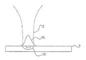
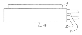
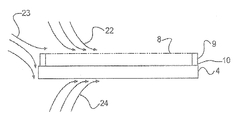
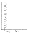
Images


Classifications
-
- B—PERFORMING OPERATIONS; TRANSPORTING
- B08—CLEANING
- B08B—CLEANING IN GENERAL; PREVENTION OF FOULING IN GENERAL
- B08B7/00—Cleaning by methods not provided for in a single other subclass or a single group in this subclass
- B08B7/0035—Cleaning by methods not provided for in a single other subclass or a single group in this subclass by radiant energy, e.g. UV, laser, light beam or the like
- B08B7/0042—Cleaning by methods not provided for in a single other subclass or a single group in this subclass by radiant energy, e.g. UV, laser, light beam or the like by laser
-
- G—PHYSICS
- G03—PHOTOGRAPHY; CINEMATOGRAPHY; ANALOGOUS TECHNIQUES USING WAVES OTHER THAN OPTICAL WAVES; ELECTROGRAPHY; HOLOGRAPHY
- G03F—PHOTOMECHANICAL PRODUCTION OF TEXTURED OR PATTERNED SURFACES, e.g. FOR PRINTING, FOR PROCESSING OF SEMICONDUCTOR DEVICES; MATERIALS THEREFOR; ORIGINALS THEREFOR; APPARATUS SPECIALLY ADAPTED THEREFOR
- G03F1/00—Originals for photomechanical production of textured or patterned surfaces, e.g., masks, photo-masks, reticles; Mask blanks or pellicles therefor; Containers specially adapted therefor; Preparation thereof
- G03F1/68—Preparation processes not covered by groups G03F1/20 - G03F1/50
- G03F1/82—Auxiliary processes, e.g. cleaning or inspecting
-
- Y—GENERAL TAGGING OF NEW TECHNOLOGICAL DEVELOPMENTS; GENERAL TAGGING OF CROSS-SECTIONAL TECHNOLOGIES SPANNING OVER SEVERAL SECTIONS OF THE IPC; TECHNICAL SUBJECTS COVERED BY FORMER USPC CROSS-REFERENCE ART COLLECTIONS [XRACs] AND DIGESTS
- Y10—TECHNICAL SUBJECTS COVERED BY FORMER USPC
- Y10S—TECHNICAL SUBJECTS COVERED BY FORMER USPC CROSS-REFERENCE ART COLLECTIONS [XRACs] AND DIGESTS
- Y10S134/00—Cleaning and liquid contact with solids
- Y10S134/902—Semiconductor wafer
Landscapes
- Physics & Mathematics (AREA)
- Optics & Photonics (AREA)
- General Physics & Mathematics (AREA)
- Preparing Plates And Mask In Photomechanical Process (AREA)
- Cleaning Or Drying Semiconductors (AREA)
- Exposure And Positioning Against Photoresist Photosensitive Materials (AREA)
Applications Claiming Priority (4)
| Application Number | Priority Date | Filing Date | Title |
|---|---|---|---|
| US95498907P | 2007-08-09 | 2007-08-09 | |
| US60/954,989 | 2007-08-09 | ||
| US12/055,178 | 2008-03-25 | ||
| US12/055,178 US7993464B2 (en) | 2007-08-09 | 2008-03-25 | Apparatus and method for indirect surface cleaning |
Publications (1)
| Publication Number | Publication Date |
|---|---|
| KR20100083125A true KR20100083125A (ko) | 2010-07-21 |
Family
ID=40341647
Family Applications (1)
| Application Number | Title | Priority Date | Filing Date |
|---|---|---|---|
| KR1020107005270A Ceased KR20100083125A (ko) | 2007-08-09 | 2008-07-30 | 간접적 표면 세정 장치 및 방법 |
Country Status (5)
| Country | Link |
|---|---|
| US (5) | US7993464B2 (enExample) |
| EP (1) | EP2178655B1 (enExample) |
| JP (1) | JP5174910B2 (enExample) |
| KR (1) | KR20100083125A (enExample) |
| WO (1) | WO2009020808A1 (enExample) |
Cited By (1)
| Publication number | Priority date | Publication date | Assignee | Title |
|---|---|---|---|---|
| WO2021003288A1 (en) * | 2019-07-02 | 2021-01-07 | Entegris, Inc. | Methods of using laser energy to remove particles from a surface |
Families Citing this family (33)
| Publication number | Priority date | Publication date | Assignee | Title |
|---|---|---|---|---|
| US11311917B2 (en) * | 2007-08-09 | 2022-04-26 | Bruker Nano, Inc. | Apparatus and method for contamination identification |
| EP2077467B9 (fr) | 2008-01-04 | 2014-09-03 | Adixen Vacuum Products | Procédé de fabrication de photomasques et dispositif pour sa mise en oeuvre |
| KR101253825B1 (ko) * | 2008-03-05 | 2013-04-12 | 알까뗄 루슨트 | 포토마스크 제조 방법 |
| JP2009244686A (ja) * | 2008-03-31 | 2009-10-22 | Fujitsu Microelectronics Ltd | フォトマスクの処理方法及び装置 |
| JP5478145B2 (ja) * | 2009-08-18 | 2014-04-23 | 東京エレクトロン株式会社 | ポリマー除去装置およびポリマー除去方法 |
| JP2011066259A (ja) * | 2009-09-18 | 2011-03-31 | Toshiba Corp | マスク洗浄方法及びマスク洗浄装置 |
| US8987632B2 (en) * | 2009-10-09 | 2015-03-24 | The United States Of America As Represented By The Administrator Of The National Aeronautics And Space Administration | Modification of surface energy via direct laser ablative surface patterning |
| US8658937B2 (en) * | 2010-01-08 | 2014-02-25 | Uvtech Systems, Inc. | Method and apparatus for processing substrate edges |
| US20110147350A1 (en) * | 2010-12-03 | 2011-06-23 | Uvtech Systems Inc. | Modular apparatus for wafer edge processing |
| US20130126467A1 (en) * | 2011-11-18 | 2013-05-23 | Shenzhen China Star Optoelectronics Technology Co., Ltd. | Method for manufacturing conductive lines with small line-to-line space |
| US9278374B2 (en) | 2012-06-08 | 2016-03-08 | The United States Of America As Represented By The Administrator Of The National Aeronautics And Space Administration | Modified surface having low adhesion properties to mitigate insect residue adhesion |
| TW201422320A (zh) * | 2012-12-03 | 2014-06-16 | Gudeng Prec Industral Co Ltd | 光罩之吹氣清潔系統及其清潔方法 |
| KR20140130963A (ko) * | 2013-05-02 | 2014-11-12 | 삼성디스플레이 주식회사 | 유기물 세정 장치 및 세정 방법 |
| KR101461437B1 (ko) * | 2013-05-27 | 2014-11-18 | 에이피시스템 주식회사 | 포토마스크 세정 장치 및 이를 이용한 포토마스크 세정 방법 |
| KR102402035B1 (ko) | 2014-11-14 | 2022-05-26 | 삼성전자주식회사 | 펠리클을 포함하는 마스크, 펠리클 리페어 장치, 및 기판 제조 설비 |
| JP2018508048A (ja) * | 2015-03-12 | 2018-03-22 | レイヴ リミテッド ライアビリティ カンパニー | 間接的表面清浄化装置および方法 |
| JP6565473B2 (ja) * | 2015-08-20 | 2019-08-28 | 大日本印刷株式会社 | 露光用マスクおよびその管理方法 |
| KR20170025100A (ko) * | 2015-08-27 | 2017-03-08 | 삼성전자주식회사 | 포토 마스크 세정 장치 |
| KR102661452B1 (ko) | 2015-10-14 | 2024-04-26 | 파이버린 테크놀로지스 리미티드 | 3d-성형 가능한 시트 물질 |
| TWI619937B (zh) * | 2016-01-15 | 2018-04-01 | 奇美視像科技股份有限公司 | 以多光子激發技術檢查物體之方法以及量測物體之裝置 |
| DE102016206088A1 (de) * | 2016-04-12 | 2017-05-24 | Carl Zeiss Smt Gmbh | Verfahren zum Bestimmen der Dicke einer kontaminierenden Schicht und/oder der Art eines kontaminierenden Materials, optisches Element und EUV-Lithographiesystem |
| US9958771B2 (en) * | 2016-06-23 | 2018-05-01 | Rave Llc | Method and apparatus for pellicle removal |
| KR102500603B1 (ko) * | 2017-01-06 | 2023-02-17 | 레이브 엘엘씨 | 오염 식별 장치 및 방법 |
| WO2018145001A1 (en) * | 2017-02-06 | 2018-08-09 | Planar Semiconductor, Inc. | Subnanometer-level light-based substrate cleaning mechanism |
| WO2019024091A1 (zh) * | 2017-08-04 | 2019-02-07 | 深圳市柔宇科技有限公司 | 激光修复方法和激光修复设备 |
| CN108160617B (zh) * | 2017-12-12 | 2021-04-30 | 深圳市华星光电半导体显示技术有限公司 | 清洁装置 |
| US10898932B2 (en) * | 2018-02-12 | 2021-01-26 | Suss Micro Tec Photomask Equipment Gmbh & Co Kg | Method and apparatus for cleaning a substrate and computer program product |
| JP7597993B2 (ja) * | 2020-01-21 | 2024-12-11 | 横浜ゴム株式会社 | 加硫用モールドの洗浄方法 |
| CN111940423B (zh) * | 2020-08-07 | 2021-07-13 | 武汉金顿激光科技有限公司 | 一种飞机非导电复合涂层的原位激光清洗方法 |
| KR20220049651A (ko) | 2020-10-14 | 2022-04-22 | 삼성전자주식회사 | 극자외선(euv) 포토마스크 제조 방법, 포토마스크 보정 방법 및 장치 |
| KR20220125832A (ko) * | 2021-03-03 | 2022-09-15 | 삼성전자주식회사 | Euv 마스크 검사 시스템 및 이를 이용한 euv 마스크 검사 방법 |
| US11822231B2 (en) * | 2021-03-30 | 2023-11-21 | Taiwan Semiconductor Manufacturing Company Ltd. | Method for removing particles from pellicle and photomask |
| DE102021120747B4 (de) | 2021-08-10 | 2024-07-11 | Carl Zeiss Sms Ltd. | Verfahren zur Entfernung eines Partikels von einem Maskensystem |
Family Cites Families (42)
| Publication number | Priority date | Publication date | Assignee | Title |
|---|---|---|---|---|
| US4292093A (en) | 1979-12-28 | 1981-09-29 | The United States Of America As Represented By The United States Department Of Energy | Method using laser irradiation for the production of atomically clean crystalline silicon and germanium surfaces |
| JPS6187338A (ja) * | 1984-10-05 | 1986-05-02 | Nec Corp | 多重ビ−ム照射Si表面ドライ洗浄法 |
| JPS62272258A (ja) * | 1986-05-21 | 1987-11-26 | Hitachi Ltd | 異物除去装置 |
| US5093563A (en) * | 1987-02-05 | 1992-03-03 | Hughes Aircraft Company | Electronically phased detector arrays for optical imaging |
| DE3721940A1 (de) | 1987-07-02 | 1989-01-12 | Ibm Deutschland | Entfernen von partikeln von oberflaechen fester koerper durch laserbeschuss |
| US4948937A (en) * | 1988-12-23 | 1990-08-14 | Itt Corporation | Apparatus and method for heat cleaning semiconductor material |
| US4987286A (en) | 1989-10-30 | 1991-01-22 | University Of Iowa Research Foundation | Method and apparatus for removing minute particles from a surface |
| JP2878490B2 (ja) | 1991-06-28 | 1999-04-05 | 株式会社日立製作所 | マスク修正方法及びそれに用いる装置及びマスク |
| US5814156A (en) * | 1993-09-08 | 1998-09-29 | Uvtech Systems Inc. | Photoreactive surface cleaning |
| JPH0864559A (ja) | 1994-06-14 | 1996-03-08 | Fsi Internatl Inc | 基板面から不要な物質を除去する方法 |
| AU3460895A (en) * | 1994-08-29 | 1996-03-22 | Uvtech Systems, Inc. | Surface modification processing of flat panel device substrates |
| TW285721B (enExample) * | 1994-12-27 | 1996-09-11 | Siemens Ag | |
| JP3728829B2 (ja) * | 1996-10-11 | 2005-12-21 | 株式会社ニコン | 荷電粒子線投影装置 |
| JPH1126411A (ja) * | 1997-06-30 | 1999-01-29 | Nikon Corp | 洗浄装置 |
| US6395102B1 (en) | 1997-08-25 | 2002-05-28 | Texas Instruments Incorporated | Method and apparatus for in-situ reticle cleaning at photolithography tool |
| US6573702B2 (en) | 1997-09-12 | 2003-06-03 | New Wave Research | Method and apparatus for cleaning electronic test contacts |
| US6472295B1 (en) | 1999-08-27 | 2002-10-29 | Jmar Research, Inc. | Method and apparatus for laser ablation of a target material |
| US6827816B1 (en) | 1999-12-16 | 2004-12-07 | Applied Materials, Inc. | In situ module for particle removal from solid-state surfaces |
| US6279249B1 (en) | 1999-12-30 | 2001-08-28 | Intel Corporation | Reduced particle contamination manufacturing and packaging for reticles |
| WO2001080606A1 (en) * | 2000-04-14 | 2001-10-25 | Macquarie Research Ltd | Methods and systems for providing emission of incoherent radiation and uses therefor |
| JP2001300450A (ja) * | 2000-04-21 | 2001-10-30 | Toshiba Corp | 洗浄装置および洗浄方法、レチクルの製造方法 |
| US6805751B2 (en) | 2000-07-24 | 2004-10-19 | Alkansas State University | Method and apparatus for removal of minute particles from a surface using thermophoresis to prevent particle redeposition |
| US6500268B1 (en) | 2000-08-18 | 2002-12-31 | Silicon Genesis Corporation | Dry cleaning method |
| KR100421038B1 (ko) | 2001-03-28 | 2004-03-03 | 삼성전자주식회사 | 표면으로부터 오염물을 제거하는 세정 장비 및 이를이용한 세정 방법 |
| US6665065B1 (en) | 2001-04-09 | 2003-12-16 | Advanced Micro Devices, Inc. | Defect detection in pellicized reticles via exposure at short wavelengths |
| US6799584B2 (en) | 2001-11-09 | 2004-10-05 | Applied Materials, Inc. | Condensation-based enhancement of particle removal by suction |
| US7253901B2 (en) * | 2002-01-23 | 2007-08-07 | Kla-Tencor Technologies Corporation | Laser-based cleaning device for film analysis tool |
| JP2003302745A (ja) * | 2002-04-12 | 2003-10-24 | Dainippon Printing Co Ltd | 異物の無害化方法 |
| US6968850B2 (en) | 2002-07-15 | 2005-11-29 | Intel Corporation | In-situ cleaning of light source collector optics |
| KR100563102B1 (ko) | 2002-09-12 | 2006-03-27 | 에이에스엠엘 네델란즈 비.브이. | 표면들로부터 입자들을 제거함으로써 세정하는 방법,세정장치 및 리소그래피투영장치 |
| US6829035B2 (en) * | 2002-11-12 | 2004-12-07 | Applied Materials Israel, Ltd. | Advanced mask cleaning and handling |
| JP2004226717A (ja) | 2003-01-23 | 2004-08-12 | Renesas Technology Corp | マスクの製造方法および半導体集積回路装置の製造方法 |
| US6874510B2 (en) | 2003-02-07 | 2005-04-05 | Lsi Logic Corporation | Method to use a laser to perform the edge clean operation on a semiconductor wafer |
| US7115514B2 (en) | 2003-10-02 | 2006-10-03 | Raydiance, Inc. | Semiconductor manufacturing using optical ablation |
| US7251033B1 (en) | 2004-06-02 | 2007-07-31 | Advanced Micro Devices, Inc. | In-situ reticle contamination detection system at exposure wavelength |
| US7230695B2 (en) * | 2004-07-08 | 2007-06-12 | Asahi Glass Company, Ltd. | Defect repair device and defect repair method |
| US7435665B2 (en) * | 2004-10-06 | 2008-10-14 | Okmetic Oyj | CVD doped structures |
| JP4681849B2 (ja) * | 2004-10-22 | 2011-05-11 | キヤノン株式会社 | 除去装置、当該除去装置を有する露光装置、デバイス製造方法 |
| TWI270504B (en) * | 2004-12-15 | 2007-01-11 | Gudeng Prec Ind Co Ltd | Photo-mask protection film frame |
| JP2006344718A (ja) * | 2005-06-08 | 2006-12-21 | Sony Corp | 異物除去方法 |
| US20080044740A1 (en) * | 2006-08-21 | 2008-02-21 | Taiwan Semiconductor Manufacturing Company, Ltd. | Photomask having haze reduction layer |
| US20080241711A1 (en) * | 2007-03-30 | 2008-10-02 | Yun Henry K | Removal and prevention of photo-induced defects on photomasks used in photolithography |
-
2008
- 2008-03-25 US US12/055,178 patent/US7993464B2/en active Active
- 2008-07-30 WO PCT/US2008/071546 patent/WO2009020808A1/en not_active Ceased
- 2008-07-30 EP EP08796835.0A patent/EP2178655B1/en active Active
- 2008-07-30 JP JP2010520148A patent/JP5174910B2/ja active Active
- 2008-07-30 KR KR1020107005270A patent/KR20100083125A/ko not_active Ceased
- 2008-11-24 US US12/277,106 patent/US8293019B2/en active Active
-
2012
- 2012-10-22 US US13/657,847 patent/US8613803B2/en active Active
-
2013
- 2013-11-11 US US14/077,028 patent/US8741067B2/en active Active
-
2014
- 2014-06-03 US US14/294,728 patent/US8986460B2/en active Active
Cited By (1)
| Publication number | Priority date | Publication date | Assignee | Title |
|---|---|---|---|---|
| WO2021003288A1 (en) * | 2019-07-02 | 2021-01-07 | Entegris, Inc. | Methods of using laser energy to remove particles from a surface |
Also Published As
| Publication number | Publication date |
|---|---|
| WO2009020808A1 (en) | 2009-02-12 |
| JP5174910B2 (ja) | 2013-04-03 |
| US20130276818A1 (en) | 2013-10-24 |
| US20140283873A1 (en) | 2014-09-25 |
| EP2178655B1 (en) | 2018-09-19 |
| US8293019B2 (en) | 2012-10-23 |
| US8986460B2 (en) | 2015-03-24 |
| JP2010536066A (ja) | 2010-11-25 |
| US20090065024A1 (en) | 2009-03-12 |
| US7993464B2 (en) | 2011-08-09 |
| US20140069457A1 (en) | 2014-03-13 |
| EP2178655A1 (en) | 2010-04-28 |
| US8613803B2 (en) | 2013-12-24 |
| EP2178655A4 (en) | 2014-05-07 |
| US20090038637A1 (en) | 2009-02-12 |
| US8741067B2 (en) | 2014-06-03 |
Similar Documents
| Publication | Publication Date | Title |
|---|---|---|
| KR20100083125A (ko) | 간접적 표면 세정 장치 및 방법 | |
| US8182609B1 (en) | Apparatus and method for direct surface cleaning | |
| JP7416863B2 (ja) | 間接的表面清浄化装置および方法 | |
| US11311917B2 (en) | Apparatus and method for contamination identification | |
| KR102500603B1 (ko) | 오염 식별 장치 및 방법 | |
| KR101365315B1 (ko) | 포토마스크의 사용 수명 증가 방법 및 포토마스크의 광학적 특성 개선 방법 | |
| JP4778542B2 (ja) | リソグラフィ装置、放射システム、デバイス製造方法、及び放射生成方法 | |
| US10898932B2 (en) | Method and apparatus for cleaning a substrate and computer program product | |
| TW202347021A (zh) | 表膜清潔系統 | |
| CN118613764A (zh) | 表膜清洁系统 |
Legal Events
| Date | Code | Title | Description |
|---|---|---|---|
| PA0105 | International application |
Patent event date: 20100309 Patent event code: PA01051R01D Comment text: International Patent Application |
|
| PG1501 | Laying open of application | ||
| A201 | Request for examination | ||
| PA0201 | Request for examination |
Patent event code: PA02012R01D Patent event date: 20110816 Comment text: Request for Examination of Application |
|
| PA0302 | Request for accelerated examination |
Patent event date: 20110816 Patent event code: PA03022R01D Comment text: Request for Accelerated Examination |
|
| PE0902 | Notice of grounds for rejection |
Comment text: Notification of reason for refusal Patent event date: 20111214 Patent event code: PE09021S01D |
|
| E601 | Decision to refuse application | ||
| PE0601 | Decision on rejection of patent |
Patent event date: 20120817 Comment text: Decision to Refuse Application Patent event code: PE06012S01D Patent event date: 20111214 Comment text: Notification of reason for refusal Patent event code: PE06011S01I |
|
| J201 | Request for trial against refusal decision | ||
| PJ0201 | Trial against decision of rejection |
Patent event date: 20121119 Comment text: Request for Trial against Decision on Refusal Patent event code: PJ02012R01D Patent event date: 20120817 Comment text: Decision to Refuse Application Patent event code: PJ02011S01I Appeal kind category: Appeal against decision to decline refusal Appeal identifier: 2012101009668 Request date: 20121119 |
|
| J501 | Disposition of invalidation of trial | ||
| PJ0501 | Disposition of invalidation of trial |
Appeal kind category: Appeal against decision to decline refusal Request date: 20121119 Appeal identifier: 2012101009668 |