US8182609B1 - Apparatus and method for direct surface cleaning - Google Patents
Apparatus and method for direct surface cleaning Download PDFInfo
- Publication number
- US8182609B1 US8182609B1 US12/188,564 US18856408A US8182609B1 US 8182609 B1 US8182609 B1 US 8182609B1 US 18856408 A US18856408 A US 18856408A US 8182609 B1 US8182609 B1 US 8182609B1
- Authority
- US
- United States
- Prior art keywords
- substrate
- pellicle
- photomask
- laser
- cleaning
- Prior art date
- Legal status (The legal status is an assumption and is not a legal conclusion. Google has not performed a legal analysis and makes no representation as to the accuracy of the status listed.)
- Active, expires
Links
- 238000000034 method Methods 0.000 title claims abstract description 204
- 238000004140 cleaning Methods 0.000 title claims abstract description 96
- 239000000758 substrate Substances 0.000 claims abstract description 123
- 239000002245 particle Substances 0.000 claims abstract description 38
- 238000005979 thermal decomposition reaction Methods 0.000 claims abstract description 6
- 238000011109 contamination Methods 0.000 claims description 59
- 239000010408 film Substances 0.000 claims description 50
- 230000006378 damage Effects 0.000 claims description 36
- 230000001965 increasing effect Effects 0.000 claims description 19
- BFNBIHQBYMNNAN-UHFFFAOYSA-N ammonium sulfate Chemical group N.N.OS(O)(=O)=O BFNBIHQBYMNNAN-UHFFFAOYSA-N 0.000 claims description 13
- 229910052921 ammonium sulfate Inorganic materials 0.000 claims description 13
- 235000011130 ammonium sulphate Nutrition 0.000 claims description 13
- 239000010409 thin film Substances 0.000 claims description 7
- 230000005670 electromagnetic radiation Effects 0.000 claims description 5
- 238000000862 absorption spectrum Methods 0.000 claims 10
- 239000010954 inorganic particle Substances 0.000 claims 1
- 239000011800 void material Substances 0.000 claims 1
- 238000010521 absorption reaction Methods 0.000 abstract description 30
- 230000008569 process Effects 0.000 description 123
- 239000000463 material Substances 0.000 description 43
- 235000012431 wafers Nutrition 0.000 description 27
- 238000010586 diagram Methods 0.000 description 26
- 238000004519 manufacturing process Methods 0.000 description 23
- 230000002829 reductive effect Effects 0.000 description 13
- 238000009826 distribution Methods 0.000 description 12
- 239000000356 contaminant Substances 0.000 description 11
- 230000005855 radiation Effects 0.000 description 11
- 239000000853 adhesive Substances 0.000 description 10
- 230000001070 adhesive effect Effects 0.000 description 10
- 238000012545 processing Methods 0.000 description 10
- 238000005259 measurement Methods 0.000 description 9
- 230000007423 decrease Effects 0.000 description 8
- 239000010453 quartz Substances 0.000 description 8
- VYPSYNLAJGMNEJ-UHFFFAOYSA-N silicon dioxide Inorganic materials O=[Si]=O VYPSYNLAJGMNEJ-UHFFFAOYSA-N 0.000 description 8
- 230000007547 defect Effects 0.000 description 7
- 239000006096 absorbing agent Substances 0.000 description 6
- 238000001816 cooling Methods 0.000 description 6
- 238000001514 detection method Methods 0.000 description 6
- 238000003384 imaging method Methods 0.000 description 6
- 230000035939 shock Effects 0.000 description 6
- 230000008901 benefit Effects 0.000 description 5
- 238000000354 decomposition reaction Methods 0.000 description 5
- 230000000694 effects Effects 0.000 description 5
- 230000015572 biosynthetic process Effects 0.000 description 4
- 230000008859 change Effects 0.000 description 4
- 230000005284 excitation Effects 0.000 description 4
- 230000005484 gravity Effects 0.000 description 4
- 239000002184 metal Substances 0.000 description 4
- 238000000386 microscopy Methods 0.000 description 4
- 238000004611 spectroscopical analysis Methods 0.000 description 4
- 238000010276 construction Methods 0.000 description 3
- 230000007613 environmental effect Effects 0.000 description 3
- 239000007789 gas Substances 0.000 description 3
- 230000000670 limiting effect Effects 0.000 description 3
- 239000007788 liquid Substances 0.000 description 3
- 238000012544 monitoring process Methods 0.000 description 3
- 239000004065 semiconductor Substances 0.000 description 3
- 239000000126 substance Substances 0.000 description 3
- 230000002123 temporal effect Effects 0.000 description 3
- 230000003685 thermal hair damage Effects 0.000 description 3
- 230000005540 biological transmission Effects 0.000 description 2
- 230000003247 decreasing effect Effects 0.000 description 2
- 230000001627 detrimental effect Effects 0.000 description 2
- 230000002708 enhancing effect Effects 0.000 description 2
- 238000011156 evaluation Methods 0.000 description 2
- 239000007888 film coating Substances 0.000 description 2
- 238000009501 film coating Methods 0.000 description 2
- 238000011065 in-situ storage Methods 0.000 description 2
- 238000007689 inspection Methods 0.000 description 2
- 238000000608 laser ablation Methods 0.000 description 2
- 230000004807 localization Effects 0.000 description 2
- 238000002844 melting Methods 0.000 description 2
- 230000008018 melting Effects 0.000 description 2
- 239000012528 membrane Substances 0.000 description 2
- 238000012986 modification Methods 0.000 description 2
- 230000004048 modification Effects 0.000 description 2
- 230000003287 optical effect Effects 0.000 description 2
- 238000007639 printing Methods 0.000 description 2
- 230000009467 reduction Effects 0.000 description 2
- 239000007787 solid Substances 0.000 description 2
- 238000001228 spectrum Methods 0.000 description 2
- 238000012546 transfer Methods 0.000 description 2
- 238000009834 vaporization Methods 0.000 description 2
- 230000008016 vaporization Effects 0.000 description 2
- XLYOFNOQVPJJNP-UHFFFAOYSA-N water Substances O XLYOFNOQVPJJNP-UHFFFAOYSA-N 0.000 description 2
- VYZAMTAEIAYCRO-UHFFFAOYSA-N Chromium Chemical compound [Cr] VYZAMTAEIAYCRO-UHFFFAOYSA-N 0.000 description 1
- 238000004566 IR spectroscopy Methods 0.000 description 1
- 229910016006 MoSi Inorganic materials 0.000 description 1
- 238000005481 NMR spectroscopy Methods 0.000 description 1
- 238000001069 Raman spectroscopy Methods 0.000 description 1
- XUIMIQQOPSSXEZ-UHFFFAOYSA-N Silicon Chemical compound [Si] XUIMIQQOPSSXEZ-UHFFFAOYSA-N 0.000 description 1
- 238000000441 X-ray spectroscopy Methods 0.000 description 1
- 238000002679 ablation Methods 0.000 description 1
- 238000002835 absorbance Methods 0.000 description 1
- 230000001133 acceleration Effects 0.000 description 1
- 230000002411 adverse Effects 0.000 description 1
- 238000004458 analytical method Methods 0.000 description 1
- 238000004630 atomic force microscopy Methods 0.000 description 1
- 238000009529 body temperature measurement Methods 0.000 description 1
- 238000000576 coating method Methods 0.000 description 1
- 239000000112 cooling gas Substances 0.000 description 1
- 239000000110 cooling liquid Substances 0.000 description 1
- 230000001419 dependent effect Effects 0.000 description 1
- 238000000151 deposition Methods 0.000 description 1
- 238000013461 design Methods 0.000 description 1
- 230000006866 deterioration Effects 0.000 description 1
- 238000006073 displacement reaction Methods 0.000 description 1
- 239000012636 effector Substances 0.000 description 1
- 238000010894 electron beam technology Methods 0.000 description 1
- 238000005530 etching Methods 0.000 description 1
- 239000012530 fluid Substances 0.000 description 1
- 238000010438 heat treatment Methods 0.000 description 1
- 230000000977 initiatory effect Effects 0.000 description 1
- 230000003993 interaction Effects 0.000 description 1
- 238000005305 interferometry Methods 0.000 description 1
- 238000010884 ion-beam technique Methods 0.000 description 1
- 230000001788 irregular Effects 0.000 description 1
- 238000001459 lithography Methods 0.000 description 1
- 238000002595 magnetic resonance imaging Methods 0.000 description 1
- 238000007726 management method Methods 0.000 description 1
- 238000004377 microelectronic Methods 0.000 description 1
- 238000012806 monitoring device Methods 0.000 description 1
- 238000010943 off-gassing Methods 0.000 description 1
- 239000003921 oil Substances 0.000 description 1
- 239000003960 organic solvent Substances 0.000 description 1
- 239000003973 paint Substances 0.000 description 1
- 230000036961 partial effect Effects 0.000 description 1
- 238000002360 preparation method Methods 0.000 description 1
- 238000004886 process control Methods 0.000 description 1
- 238000002310 reflectometry Methods 0.000 description 1
- 230000008439 repair process Effects 0.000 description 1
- 238000001073 sample cooling Methods 0.000 description 1
- 238000000682 scanning probe acoustic microscopy Methods 0.000 description 1
- 238000004574 scanning tunneling microscopy Methods 0.000 description 1
- 230000009291 secondary effect Effects 0.000 description 1
- 230000035945 sensitivity Effects 0.000 description 1
- 238000000926 separation method Methods 0.000 description 1
- 238000007493 shaping process Methods 0.000 description 1
- 229910052710 silicon Inorganic materials 0.000 description 1
- 239000010703 silicon Substances 0.000 description 1
- 238000012306 spectroscopic technique Methods 0.000 description 1
- 238000012876 topography Methods 0.000 description 1
- 230000007704 transition Effects 0.000 description 1
- 238000000870 ultraviolet spectroscopy Methods 0.000 description 1
- 239000012808 vapor phase Substances 0.000 description 1
- 238000002424 x-ray crystallography Methods 0.000 description 1
Images


Classifications
-
- B—PERFORMING OPERATIONS; TRANSPORTING
- B08—CLEANING
- B08B—CLEANING IN GENERAL; PREVENTION OF FOULING IN GENERAL
- B08B7/00—Cleaning by methods not provided for in a single other subclass or a single group in this subclass
- B08B7/0035—Cleaning by methods not provided for in a single other subclass or a single group in this subclass by radiant energy, e.g. UV, laser, light beam or the like
- B08B7/0042—Cleaning by methods not provided for in a single other subclass or a single group in this subclass by radiant energy, e.g. UV, laser, light beam or the like by laser
-
- G—PHYSICS
- G03—PHOTOGRAPHY; CINEMATOGRAPHY; ANALOGOUS TECHNIQUES USING WAVES OTHER THAN OPTICAL WAVES; ELECTROGRAPHY; HOLOGRAPHY
- G03F—PHOTOMECHANICAL PRODUCTION OF TEXTURED OR PATTERNED SURFACES, e.g. FOR PRINTING, FOR PROCESSING OF SEMICONDUCTOR DEVICES; MATERIALS THEREFOR; ORIGINALS THEREFOR; APPARATUS SPECIALLY ADAPTED THEREFOR
- G03F1/00—Originals for photomechanical production of textured or patterned surfaces, e.g., masks, photo-masks, reticles; Mask blanks or pellicles therefor; Containers specially adapted therefor; Preparation thereof
- G03F1/68—Preparation processes not covered by groups G03F1/20 - G03F1/50
- G03F1/82—Auxiliary processes, e.g. cleaning or inspecting
-
- H—ELECTRICITY
- H01—ELECTRIC ELEMENTS
- H01L—SEMICONDUCTOR DEVICES NOT COVERED BY CLASS H10
- H01L21/00—Processes or apparatus adapted for the manufacture or treatment of semiconductor or solid state devices or of parts thereof
- H01L21/67—Apparatus specially adapted for handling semiconductor or electric solid state devices during manufacture or treatment thereof; Apparatus specially adapted for handling wafers during manufacture or treatment of semiconductor or electric solid state devices or components ; Apparatus not specifically provided for elsewhere
- H01L21/67005—Apparatus not specifically provided for elsewhere
- H01L21/67011—Apparatus for manufacture or treatment
- H01L21/67017—Apparatus for fluid treatment
- H01L21/67028—Apparatus for fluid treatment for cleaning followed by drying, rinsing, stripping, blasting or the like
-
- G—PHYSICS
- G03—PHOTOGRAPHY; CINEMATOGRAPHY; ANALOGOUS TECHNIQUES USING WAVES OTHER THAN OPTICAL WAVES; ELECTROGRAPHY; HOLOGRAPHY
- G03F—PHOTOMECHANICAL PRODUCTION OF TEXTURED OR PATTERNED SURFACES, e.g. FOR PRINTING, FOR PROCESSING OF SEMICONDUCTOR DEVICES; MATERIALS THEREFOR; ORIGINALS THEREFOR; APPARATUS SPECIALLY ADAPTED THEREFOR
- G03F1/00—Originals for photomechanical production of textured or patterned surfaces, e.g., masks, photo-masks, reticles; Mask blanks or pellicles therefor; Containers specially adapted therefor; Preparation thereof
- G03F1/62—Pellicles, e.g. pellicle assemblies, e.g. having membrane on support frame; Preparation thereof
-
- Y—GENERAL TAGGING OF NEW TECHNOLOGICAL DEVELOPMENTS; GENERAL TAGGING OF CROSS-SECTIONAL TECHNOLOGIES SPANNING OVER SEVERAL SECTIONS OF THE IPC; TECHNICAL SUBJECTS COVERED BY FORMER USPC CROSS-REFERENCE ART COLLECTIONS [XRACs] AND DIGESTS
- Y10—TECHNICAL SUBJECTS COVERED BY FORMER USPC
- Y10S—TECHNICAL SUBJECTS COVERED BY FORMER USPC CROSS-REFERENCE ART COLLECTIONS [XRACs] AND DIGESTS
- Y10S134/00—Cleaning and liquid contact with solids
- Y10S134/902—Semiconductor wafer
Definitions
- the present invention relates generally to devices and methods useful in cleaning surfaces. More particularly, the present invention relates to devices and methods useful in cleaning surfaces of components typically used in the semiconductor industry, optics, etc.
- Electromagnetic radiation has long been used for surface cleaning Examples of these processes include the removal of surface contamination, removal of thin material layer coatings such as paints or removal of oils from metal work surfaces. Some of the earliest examples utilized flash lamp radiation sources. These systems can be limited in application because of peak powers achievable.
- Lasers have increasingly been used for these types of processes because of the high peak powers achievable, high energy stability and wavelength selectivity. These features allow for high localization, improved material selectivity, and depth control of the cleaning effect.
- Laser surface cleaning processes can be broadly categorized into surface contamination layer removal and particulate removal. Removal of surface contamination layers is normally accomplished by laser ablation. Particle removal involves removing the contamination as a whole.
- Short pulsed radiation in particular can provide improved processing.
- Short pulsed radiation has been shown to decrease the heat affected zone in laser ablation processing. This allows improved localization of the ablative removal as well as finer control of the removal depth.
- Short pulse radiation also can enhance particulate removal by increasing the rate of thermal increase within the particles and/or substrate thereby increasing the acceleration forces that produce particle removal.
- Substrate damage can be an issue for both ablative and particulate removal processes and several techniques have been developed to minimize these effects.
- selecting a wavelength that increases the absorption of the contaminant can reduce the fluence requirement and therefore reduce substrate damage.
- using multiple pulses for full contaminant removal can reduce the required fluence.
- substrates that have high absorption at the selected wavelengths are likely to be ablated along with the contamination, even with wavelength selection and multiple pulse removal processes. The ability to end stop the removal process at the substrate interface will be limited in these cases. This problem is significantly increased for smaller size contamination, since the absorption cross section for the contamination is reduced relative to the substrate.
- particulate removal processes can also cause substrate damage for sensitive substrates and substrates that have high absorption at the processing wavelength. This problem is increased for small particle removal because of increased adhesion forces between the particles and substrate and self focusing of the laser underneath the particles.
- the developed methods for reducing the risk of substrate damage involve controlling the environment above the contaminated surface. Examples of particulate laser processes allowing reduced fluence levels include wet laser cleaning, steam laser cleaning, and increased humidity cleaning. Combinations of laser and other cleaning process (including etching, organic solvents, and ultrasonic) have been shown to increase cleaning effectiveness and may reduce the risk of substrate damage.
- all of the particulate removal processes described require access to the environment above the substrate surface. This may be impractical for some systems.
- Laser acoustic wave cleaning and laser shock wave cleaning are dry laser cleaning methods that have also been evaluated for particulate cleaning
- Laser acoustic wave cleaning involves direct excitation to the substrate and therefore suffers from a high potential for substrate damage particularly for small particles as discussed.
- Laser shock wave cleaning has been shown to improve particulate removal and can reduce the risk of substrate damage by focusing the laser above the substrate surface and relying on the shock wave interaction with the particulates. This technique will also have increased difficulty when applied to small particle removal.
- the shock wave may damage other sensitive features on or near the surface of the substrate. This is particularly true if there is a sensitive material above the substrate surface, since generating the shock wave requires relatively high laser intensity focused above the substrate.
- Semiconductor manufacturing is one of the major industrial areas that utilize surface cleaning processes including laser cleaning methods. Many of the required cleaning processes have a stringent tolerance on the allowable level of substrate damage. In addition, the small product features make it necessary to remove very small particles avoid product failures. Cleaning is an issue in multiple wafer processing steps and includes extended contamination layer (i.e. resist removal) and particulate contamination removal.
- Haze formation is a problem for the wafer print process because as the particles increase in size they block more of the light being transmitted through the photomask. Eventually the haze contamination absorbs enough of the light to cause defects in the printed image of the photomask on the wafer. Before the haze contamination reaches this level, the photomask surface must be cleaned. This cleaning requirement has the affect of decreasing the useable lifetime of a photomask because the processes currently used to remove haze deteriorate the absorbing film on the mask. Duplicate sets of photomasks must be made in order to continue manufacturing once the useable life of a photomask is exceeded. Duplicate sets are also required for use while contaminated photomask are being cleaned.
- a pellicle consists of a frame that is adhesively bonded to the photomask surface and a thin membrane stretched across the pellicle frame. Pellicles are used to prevent externally generated particles from settling onto the surface of the photomask where they could affect the print process. Externally generated particles settle on the membrane above the mask surface where they have a significantly reduced affect on the print process. With the exception of a small valve on the pellicle frame to allow for pressure equalization, the top surface of the photomask is effectively sealed from the local environment by the pellicle attachment.
- the current accepted method for haze removal requires the wafer manufacture to ship the contaminated photomask back to the mask maker or to a third party.
- the pellicle frame is removed from the photomask, the mask is cleaned, inspected for defects and a new pellicle is attached to the photomask and in many cases the mask is inspected again for particle defects before it is shipped back to the wafer manufacture.
- there is a small probability usually due to adhesive from the pellicle being removed and falling onto printable areas of the photomask, that the mask will be damaged beyond use by the haze removal process.
- Embodiments of the present invention provide a method for cleaning a surface of a substrate that includes directing a laser towards at least one radiation-produced particle disposed on a substrate, generating a thermal increase in the particle and removing the particle from the substrate by thermal decomposition.
- the laser has a wavelength that substantially coincides with a high absorption coefficient of the particle.
- the substrate is at least partially enclosed within a pellicle and the laser is directed through the pellicle film.
- FIG. 1 For embodiments of the present invention, provide a method for increasing the useable lifetime of a photomask substrate that includes directing electromagnetic radiation towards a radiation-produced contamination on a photomask substrate, generating a thermal increase in the contamination, and removing at least a portion of the contamination by thermal decomposition.
- the electromagnetic radiation has a wavelength that substantially coincides with a high absorption coefficient of the contamination.
- FIG. 1 a illustrates a schematic diagram of laser excitation and surface contamination, in accordance with an embodiment of the present invention.
- FIG. 1 b illustrates a schematic diagram of a substrate surface demonstrating contamination removal, in accordance with an embodiment of the present invention.
- multiple species may be removed from the mask in the form of a gas, liquid/solid vapor, etc.
- FIG. 2 illustrates a diagram of a photomask surface with thin film absorber on top including contamination on the film and on the substrate, in accordance with an embodiment of the present invention.
- FIG. 3 illustrates a plot of ammonium sulfate absorption in the near to mid infrared region of the electromagnetic spectrum, in accordance with an embodiment of the present invention.
- FIG. 4 illustrates a diagram of a photomask surface with thin film absorber including pellicle attached to surface, in accordance with an embodiment of the present invention. According to certain embodiments of the present invention, contamination may be present on the film and/or on the substrate.
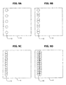
- FIG. 5 a illustrates a schematic diagram of a photomask with a pellicle showing laser beam focused through the pellicle and onto the surface, in accordance with an embodiment of the present invention.
- FIG. 5 b illustrates a schematic diagram of the beam spot size on the pellicle versus on the mask produced by focusing, in accordance with an embodiment of the present invention.
- FIG. 5 c illustrates a schematic diagram of a photomask with a pellicle showing laser beam focused through the pellicle and onto the surface and a side view of the beam spot on the pellicle, in accordance with an embodiment of the present invention.
- FIG. 6 a illustrates a cross sectional view of a Gaussian beam energy distribution and the corresponding temperature profile produced, in accordance with an embodiment of the present invention.
- FIG. 6 b illustrates a cross sectional view of a top-hat beam energy distribution and the corresponding temperature profile produced, in accordance with an embodiment of the present invention.
- this top-hat distribution differs from a Gaussian, flat top distribution.
- FIG. 7 illustrates a diagram of a photomask with a cold plate contacting the bottom of mask, in accordance with an embodiment of the present invention.
- the contact point that may be for example water, a fluid or gas that flows through the cold plate or electrical contact for thermoelectric cooling.
- FIG. 8 illustrates a diagram showing force air cooling of areas on the photomask, in accordance with an embodiment of the present invention.
- FIG. 9 a illustrates a diagram showing a single pass of the laser beam across surface to minimize local thermal build up, in accordance with an embodiment of the present invention.
- a single row or column with large lateral spacing between spots is illustrated.
- FIG. 9 b illustrates a diagram showing two passes of the laser beam across surface to minimize local thermal build up, in accordance with an embodiment of the present invention.
- a single row with two sets of beam spots overlapped with large spacing between sets of pulses is illustrated.
- FIG. 9 c illustrates a diagram showing multiple laser passes over an area of the substrate to achieve complete cleaning of the section of the substrate, in accordance with an embodiment of the present invention.
- FIG. 9 d illustrates a diagram illustrating second dimension of surface cleaning, in accordance with an embodiment of the present invention.
- FIG. 9 e illustrates a diagram representing the use of non-contiguous pulses on the surface, in accordance with an embodiment of the present invention.
- FIG. 10 illustrates a diagram employing a laser pulse pattern to control the location of residual materials, in accordance with an embodiment of the present invention.
- FIG. 11 a illustrates a diagram demonstrating the use of gravity to control the location of residual materials, in accordance with an embodiment of the present invention.
- FIG. 11 b illustrates a diagram illustrating the use of gravity to control the location of residual materials, in accordance with an embodiment of the present invention.
- FIG. 12 illustrates a schematic diagram of contaminated substrate surface with thermocouple or infrared temperature monitoring devices, in accordance with an embodiment of the present invention.
- FIG. 13 illustrates a schematic diagram of contaminated substrate surface with imaging, microscopy or spectroscopy system for contamination analysis, in accordance with an embodiment of the present invention.
- FIG. 14 illustrates a schematic diagram of a contaminated substrate surface with an imaging system where imaging system and laser beam delivery common paths, in accordance with an embodiment of the present invention.
- FIG. 15 illustrates a system diagram showing robotic load and X/Y/Z stage motion of substrate relative to laser beam, in accordance with an embodiment of the present invention.
- FIG. 16 a illustrates a box diagram of typical wafer fabrication process utilizing photomask wet clean processing, in accordance with an embodiment of the present invention.
- FIG. 16 b illustrates a box diagram of wafer fabrication process flow incorporating use laser photomask cleaning without pellicle removal, in accordance with an embodiment of the present invention.
- FIG. 16 c illustrates a box diagram of wafer fabrication process flow incorporating use of laser photomask cleaning without the use of additional mask sets during the clean process, in accordance with an embodiment of the present invention.
- a method for laser surface cleaning is provided where access to the environment above the substrate surface has limited or no access.
- the method typically includes the direct laser excitation of a contaminating particulate or contamination layer on a substrate surface ( FIG. 1 a ), where ( 1 ) is the laser, ( 2 ) is the laser beam, ( 3 ) are the particulates or layer contamination to be removed and ( 4 ) is the substrate.
- the contaminating particulate or contamination layer may be, for example, inorganic.
- energy sources other than laser may also be used (e.g., lamps and other devices that can radiate energy all along the electromagnetic spectrum may be used, including generators of gamma rays, x-rays, ultraviolet light, visible light, infrared radiation, microwave radiation, radio waves, etc.)
- the excitation increases the temperature within the contaminant and produces a thermally based removal ( FIG. 1 b ), including but not limited to vaporization ( 5 ) and decomposition ( 6 ).
- the method provides a particular advantage but is not limited to applications where the environment above the contaminated substrate is substantially or fully enclosed. In these cases, the method may also include directing the laser beam through a material disposed relative to the surface that is part of the substrate's environmental enclosure.
- the method may include the use of contamination ablation and/or the use of shock waves generated above the contaminated substrate surface.
- the alternative embodiments may include directing the beam through a material disposed relative to the surface that is part of the substrates environmental enclosure. It should be noted that the processes used in methods according to some of embodiments of the present invention may sometimes also be applicable to alternate embodiments of the present invention.
- the method has a reduced risk of substrate damage because it relies on a thermal based removal of the contamination.
- the primary reduction in the risk of substrate damage over other known techniques is typically due to the relatively low temperature requirement for the thermal removal process compared to the thermal damage thresholds for the substrate material(s).
- the risk of substrate damage is also sometimes reduced because the nominal pulse-width requirements are commonly relatively long so the potential for multi-photon absorption processes is reduced.
- the method provides for improved removal of small contaminants/particles because of the reduced fluence allowed by the lower temperature requirement.
- Methods according to certain embodiments of the present invention include selecting a laser wavelength that coincides with a strong absorption of the contaminating species and/or a weak absorption of the substrate and setting the laser energy and pulse width to produce the desired cleaning effect.
- Increased absorption in the contaminant will typically allow lower laser energies to be used for the clean process and therefore, can decrease the potential for substrate damage. This may become particularly important when the substrate materials are highly absorbing at the selected wavelength.
- the use of multiple laser wavelengths in the cleaning process may be employed, if more than one contaminating species is present or if the contaminant species has multiple high absorbance components. Multiple wavelengths may also be used for the same component if it undergoes a material or material properties change during a first step of the cleaning process. Multiple wavelengths may be produced by utilizing multiple laser sources or a single tunable laser source or both.
- Control of the laser beam parameters is sometimes critical in the application of the invention to photomask surface cleaning of haze contamination. Wavelength selection may also sometimes be critical because of the physical structure of the typical photomask.
- a photomask FIG. 2
- a photomask consists of a quartz substrate ( 4 ) with a thin absorbing film ( 7 ) on the critical surface.
- a metal film there will typically be a significant absorption coefficient for the majority of producible laser wavelengths.
- the substrate (quartz) in this example is by design transmitting in the wavelength range used for the lithography process. There will typically be a significant range from the UV to the mid IR wavelength range where the quartz substrate will be weakly absorbing, because of the purity of the quartz materials used.
- a specific example of a method according to the present invention includes the removal of ammonium sulfate haze from the surface of a photomask.
- ammonium sulfate is expected to decompose at temperatures above 280° C.
- the lowest thermal damage point for a typical photomask according to this embodiment will be the melting/reflow point for the base quartz substrate (i.e., around 1600° C.). Therefore, there is a potential process where the temperature for contamination removal/cleaning can occur that is below the damage level of the substrate materials.
- the relative absorption in the ammonium sulfate and in the photomask substrate and film material should typically be considered.
- Ammonium sulfate has several significant absorption peaks in the Mid IR wavelength range ( FIG. 3 ). Selecting one of the wavelengths, for example around 3 um, 7 um or 9 um, would increase the absorption in the ammonium sulfate and decrease the risk of damage to the film or substrate. If the photomask has a metal film layer (i.e. chrome), there could be an advantage to selecting one of the longer wavelength absorption peaks (i.e. 7 ⁇ m or 9 um), because the reflectivity of the metal film increases with increasing wavelength in this region. This reduces the light available to be absorbed by the film.
- a metal film layer i.e. chrome
- the 7 ⁇ m wavelength it may be preferable to use the 7 ⁇ m wavelength because there is a significant quartz absorption in the 9 ⁇ m wavelength range.
- the photomask had a partially absorbing film coating (i.e. MoSi) it could become advantageous to use a laser wavelength around the 3 ⁇ m absorption of ammonium sulfate. At this wavelength, both the film and the quartz are very weak absorbers and a higher intensity could be used for cleaning without risk of substrate damage.
- the 3 ⁇ m wavelength range could become advantageous to use for an ablative removal cleaning of ammonium sulfate since this process typically requires a very weak absorption of the substrate materials to avoid damage.
- the process just described for use according to certain embodiments of the present invention could increase the useable lifetime of a photomask by replacing the current cleaning processes used to remove haze from photomask surfaces.
- low temperature laser removal of haze contamination would not in general decrease the absorber thickness and line widths of the absorber film. This loss of material limits the number of clean process that the photomask can tolerate before affecting the microelectronic devices performance.
- an unlimited number of cleaning cycles could be used with the laser clean process.
- One of the reasons that aggressive wet clean processes are used is the fact that removal of the pellicle frame from the photomask leaves an adhesive residue.
- the method applied to photomask haze cleaning does not require removal of the pellicle. Rather, the laser cleaning method is performed through the pellicle film material without affecting the pellicle film characteristics ( FIG. 4 ) where ( 8 ) is the pellicle film, ( 9 ) is the pellicle frame and ( 10 ) is the adhesive between the frame and the photomask substrate.
- the absorption of the pellicle film at the process wavelength and the energy density (fluence) at the surface of the pellicle film should be considered.
- the cleaning process typically does not produce a temperature increase in the pellicle film that is above the damage threshold.
- ⁇ T is the temperature change within the material and F is the absorbed laser fluence.
- F is the fluence
- E is the energy
- r is the radius of the beam on the substrate surface.
- the ratio of the beam radius at the pellicle to the beam radius on the mask surface is typically increased by focusing the beam through the pellicle and, therefore, the relative fluence on the pellicle film compared to the photomask substrate surface can be reduced ( FIG. 5 b ).
- ( 13 ) is the laser beam diameter at the substrate surface and ( 14 ) is the diameter at the pellicle film.
- the pulse width, temporal pulse shape and the spatial distribution of the laser may be used to enhance the cleaning process or increase the safe operation range for processing.
- Shorter pulse widths can be used to minimize the overall thermal input to the system (substrate and contamination).
- Longer pulse widths may be used to maintain the process temperature for an extended period of time enhancing the completeness of the thermal removal process.
- the temporal pulse shape can be used to control the temperature rise within the contaminating species.
- a long temperature rise may be used to produce an initial effect (such as melting) that would be followed by a secondary effect (such as decomposition).
- a shorter rise time enhances vaporization of the contaminant while limiting the decomposition processes.
- Combinations of short and long temporal pulse shape can also be used to optimize the removal process.
- the use of multiple pulses can also be used to lower beam energy required for complete cleaning further decreasing the risk of substrate damage.
- the spatial distribution of the laser beam can be used to increase the process window.
- FIG. 6A shows a typical Gaussian spatial distribution ( 15 ), that may produce a temperature gradient in the substrate ( 16 ) while ( FIG. 6B ) has a flat top or top hat spatial distribution ( 17 ) allowing for a more uniform temperature rise within the substrate ( 18 ).
- the spatial distribution can be used to increase the process window. For example, having a flat top or top hat spatial distribution allows for a uniform temperature rise within the beam spot, whereas a Gaussian distribution may produce a temperature gradient within the beam spot.
- the maximum energy in the beam is limited by the peak of the Gaussian distribution. Therefore, either the risk of substrate damage may be increased or the available cleaning area within the beam (which is proportional to the cleaning efficiency) will be reduced.
- certain embodiment of the present invention include a thermal based process, it may be desirable to manage the overall temperature of the system to avoid damage to thermally sensitive or easily contaminated materials. This is particularly true in the case of photomask haze cleaning without pellicle removal.
- the pellicle films typically have a low thermal damage threshold. Therefore, it would be useful to avoid an overall system temperature build up that may transfer to and damage the pellicle material. This includes the pellicle frame and the enclosed environment between the mask surface and the pellicle film.
- Managing the system temperature can be accomplished in several ways.
- the following examples illustrate representative methods of sample cooling and it is understood that other methods may exist.
- One way to manage the system temperature is through contact cooling.
- the photomask for example, may be placed in contact with a plate that acts as a heat sink to draw the heat generated on the front surface of the mask toward the back of the mask ( FIG. 7 ).
- ( 20 ) and ( 21 ) are the input and output for the flow of cooling liquids or gases through the heat sink ( 19 ). This can reduce the heat transfer to the air above the mask surface and the heat transferred to the adhesive between the pellicle frame and the mask surface.
- This can be accomplished in a variety of ways including a cooling liquid, gas or thermoelectric cooling.
- FIG. 8 Another potential way to control temperature is through directed air flow cooling ( FIG. 8 ).
- airflow is directed onto portions of the mask ( 22 ), onto the pellicle film ( 23 ), pellicle frame or adhesives areas ( 24 ) to directly reduce the thermal build up in these materials. This not only reduces the risk of pellicle film damage but also reduces the risk of creating contaminating out-gassing from the pellicle frame and pellicle film adhesives.
- pulse to pulse thermal build is also controlled and depends on the thermal characteristics of the contamination, substrate and adjacent materials.
- pulse to pulse thermal build up is controlled by reducing the number of laser pulses hitting the surface per unit time. This temperature build up can also be controlled by increasing the distance between adjacent laser pulses.
- a large lateral displacement between adjacent pulses may be used, where the material is particularly sensitive to pulse-to-pulse thermal build (i.e. pellicle film materials).
- the process may involve positioning the laser beam to nearly the same locations multiple times to obtain full cleaning of the target surface. For example, a first series of laser pulses may be exposed to the surface with a relatively large lateral separation ( FIG. 9 a ).
- a second pass over the same area places an additional series of laser pulses that are slightly shifted relative to the first set of spots ( FIG. 9 b ). This process typically continues until the entire area has been exposed to the laser pulses ( FIG. 9 c ). Overlap in a second direction can be used to completely expose a substrate surface ( FIG. 9 d ). This overall process may be repeated or the overlap between passes may be increased, if the cleaning process includes multiple pulses for complete removal. Changing the position of the beam relative to the surface as illustrated can be accomplished by moving the beam or moving the substrate. In addition, applying pulses in a more systematically distributed manner across the mask may reduce further the likelihood of heat buildup on the mask ( FIG. 9E ).
- the inventive laser cleaning method may produce residual materials on the photomask surface depending on the decomposition products of the contamination. Even if the residues no longer affect the use of the substrate material (substrate is effectively cleaned), there may still be a reason to control there location.
- Traditional methods for controlling residue formation such as applying a directed airflow, water flow or creating a reduced pressure over the substrate to be cleaned could be used within the scope of certain embodiments of the present invention.
- an enclosed system such as a pellicalized photomask, these environmental controls typically cannot be used.
- alternative methods for controlling the location of residual materials are used for a closed system.
- One representative method includes controlling the pattern of laser pulses. For example, in ( FIG. 10 ) if the pattern of laser pulses starts in the center of the substrate surface and is directed into an increasing diameter circular ( 25 ) or increasing dimension square pattern ( 26 ), residual material will be preferentially moved toward the edges of the substrate.
- Another representative method to control residue is to utilize gravity. Placing the photomask with the surface facing down ( FIG. 11 a ) or tilted ( FIG. 11 b ) will typically allow preferential deposit of residue materials on the pellicle film ( 27 ), or side of the photomask ( 28 ), respectively.
- reducing the temperature of an area of the photomask, pellicle or pellicle frame can create preferential depositing of residue material to these surfaces, since this material is likely to be generated from a vapor phase transition to a liquid or solid ( FIG. 8 ).
- a method is provided that may also be used in combination with metrology to monitor process parameters and/or to evaluate the progression or completion of the cleaning process.
- Measurement of the locally generated temperature of the substrate materials can be used in combination with the cleaning process. Temperature measurement can, for example, be evaluated prior to application of the cleaning process in order to verify risk of temperature related damage. In addition, these temperatures may be monitored during the cleaning process to verify process control and reduce the risk of material damage. For example, the temperature of the substrate may be monitored during the process and the cleaning process may be turned off if too large a temperature build up is detected.
- Multiple methods of temperature monitoring exist ( FIG. 12 ) and include contact (e.g., thermal-couples— 29 ) and non-contact (e.g., infrared cameras— 30 ) methods.
- Metrology may also be used to analyze the contamination for material properties prior to, during or after the removal process ( FIG. 13 ).
- ( 31 ) could be optical, spectroscopic techniques or any other means that can be used to detect the contaminant. Identification of the contaminant prior to running the cleaning process can be used to set the ideal processing parameters. This allows use of the minimum process temperature reducing the risk of substrate damage.
- Monitoring the contamination during or after the process can also be used to assess the completion of the cleaning process based on the strength of the measurement signal as the cleaning process progresses.
- monitoring for alternative materials during or after the process may be used to signal when the process is creating a different contamination or causing an undesired change in the substrate material. This information may be used to control the process and/or reduce the risk of substrate damage or a poor cleaning result and determine if the photomask requires another clean with the current process or a process with different parameters/conditions.
- Metrology used to detect the presence of contamination may be used to determine whether or not to apply laser pulses to the region of the substrate that was measured. This information can then be used to minimize the number of pulses applied to the overall substrate which reduces the total thermal energy applied to the system as well as the overall cleaning process time.
- Metrology to measure the lateral size/dimensions, location, number, density and/or height (thickness) of the contamination or contaminating particles can also be used in combination with the cleaning process. These measurements can be used to qualify the efficiency and completion of the process by measurement before and after the cleaning process. During the process, these measurements can be used to evaluate the in-situ efficiency of the processes.
- the metrology may be designed to view the area being cleaned while the cleaning process is occurring. This may be done, for example, by imaging the area being exposed by the laser ( FIG. 14 ) and may or may not include using the optics such as ( 33 ) half mirror and ( 32 ) focusing for optical components. Multiple methods exist for detection of particles and evaluation of particle dimensions.
- These methods include reflected and transmitted light intensity measurement, imaging, low angle scattered light detection, interferometry, scanning electron beam microscopy, focused ion beam microscopy, scanning tunneling microscopy, near field microscopy, atomic force microscopy, infrared spectroscopy, visible spectroscopy, ultraviolet spectroscopy, X-ray spectroscopy, X-ray crystallography, photoelectric spectroscopy, auger electron spectroscopy, magnetic resonance imaging, nuclear magnetic resonance spectroscopy, Raman spectroscopy, florescence spectroscopy, etc. All of these methods, and others, are within the scope of certain embodiments of the present invention and multiple methods may be combined to provide additional information.
- multiple metrologies can be incorporated into the laser cleaning process. Identifying the presence of a specific contamination (e.g., ammonium sulfate) on a photomask, for example, can define the decomposition temperature requirement and allow selection of laser energy just high enough to perform the cleaning process. Transmitted light intensity may also be measured and the result compared with the programmed structure for the absorbing film on the photomask surface. Discrepancies between programmed features and detected features may then be used to identify contamination.
- Aerial Imaging Measurement may be used to evaluate the print characteristics of the photomask. This method is typically used to evaluate the effect of contamination on the performance of the photomask.
- This measurement is also typically used in-situ to detect damage to the absorber layer resulting from the clean process. This is particularly relevant for partially absorbing films in which the thickness of the film has a direct relationship to the photomask performance.
- combining scattered and transmitted light techniques would allow detection of irregular surface topography which would differ from the typically smooth surface of the photomask and photomask film enhancing contaminant identification.
- Metrology is also used, according to certain embodiments of the present invention, to monitor the characteristics of materials adjacent to the surface being cleaned. For example, the temperature of a pellicle film above a photomask may be monitored to reduce the risk of pellicle film damage.
- the transmission characteristics of the pellicle film may also be used to qualify the effects of the cleaning process during or after the clean process.
- detection of particulates on the inside of the pellicle film is sometimes made prior to performing the clean process and is sometimes used to detect loss of these particles during the process or whether or not there needs to be a limit of the energy used on the process to prevent the risk of pellicle or substrate material damage
- This apparatus may additionally have the capability to robotically handle the substrate material ( 35 ) with mask handling end effector ( 36 ) and/or one or more axes of motion to position the substrate sample relative to the laser beam.
- the apparatus may contain one or more of the metrologies as described above and may contain components and/or devices useful for controlling the temperature of the substrate and/or adjacent materials during the cleaning process.
- the apparatus may contain metrology used to register the substrate ( 34 ) in ( FIG. 15 ) to the staging system and therefore to the laser beam.
- This metrology may include, for example, computer controlled vision recognition systems.
- the apparatus may also utilize computer control of the laser, motion and metrology and may provide for software based recipe control of the cleaning process. Laser control may, for example, consist of controlling when laser pulses are applied as well as the amount of energy applied during the cleaning process.
- a method and/or apparatus is provided that can be used as part of a novel wafer fabrication process that includes the removal of haze formation from a pellicalized photomask surface.
- methods for cleaning silicon wafers are within the scope of certain embodiments of the present invention.
- Duplicate sets of photomasks are typically used during the time required to have the currently available photomasks cleaned and a new pellicle attached. These additional photomasks add a significant cost to the overall wafer print process because of the high material and setup and evaluation costs required.
- a novel wafer fabrication method is provided that incorporates an apparatus that implements one or more methods according to embodiments of the present invention to clean a photomask surface of haze.
- a representative wafer fabrication process according to the present invention and illustrating the use of wet clean processing to remove photomask contamination is shown in FIG. 16 a .
- An alternative embodiment of the present invention utilizes a laser cleaning method described above to perform the cleaning operation at the wafer fabrication facility and without pellicle removal ( FIG. 16 b ). This eliminates the additional pellicle costs and deterioration of the photomask film produced by the currently available wet clean processing.
- a novel wafer fabrication process that eliminates the use of additional masks or mask sets for product manufacture while the original set is being cleaned.
- the original photomask(s) can be placed immediately back into production following the cleaning process ( FIG. 16 c ). This, in some instances, eliminates the use of for duplicate mask sets and, in other instances, decreases the setup times for using duplicate mask sets.
- the use of inspection metrology to verify the cleaning process may be used prior to returning the photomask back into production. This measurement may, for example, be incorporated into the apparatus or provided by an additional apparatus at the wafer fabrication or other facility. Regardless of the metrology used, if any, the overall process time for the photomask haze removal will be reduced.
Abstract
Description
ΔT˜F (Equation 1)
F˜E/r2 (Equation 2)
Claims (18)
Priority Applications (2)
| Application Number | Priority Date | Filing Date | Title |
|---|---|---|---|
| US12/188,564 US8182609B1 (en) | 2007-08-09 | 2008-08-08 | Apparatus and method for direct surface cleaning |
| US13/475,997 US8562749B2 (en) | 2007-08-09 | 2012-05-20 | Wafer fabrication process |
Applications Claiming Priority (2)
| Application Number | Priority Date | Filing Date | Title |
|---|---|---|---|
| US95498607P | 2007-08-09 | 2007-08-09 | |
| US12/188,564 US8182609B1 (en) | 2007-08-09 | 2008-08-08 | Apparatus and method for direct surface cleaning |
Related Child Applications (1)
| Application Number | Title | Priority Date | Filing Date |
|---|---|---|---|
| US13/475,997 Continuation US8562749B2 (en) | 2007-08-09 | 2012-05-20 | Wafer fabrication process |
Publications (1)
| Publication Number | Publication Date |
|---|---|
| US8182609B1 true US8182609B1 (en) | 2012-05-22 |
Family
ID=46061220
Family Applications (2)
| Application Number | Title | Priority Date | Filing Date |
|---|---|---|---|
| US12/188,564 Active 2029-01-03 US8182609B1 (en) | 2007-08-09 | 2008-08-08 | Apparatus and method for direct surface cleaning |
| US13/475,997 Active US8562749B2 (en) | 2007-08-09 | 2012-05-20 | Wafer fabrication process |
Family Applications After (1)
| Application Number | Title | Priority Date | Filing Date |
|---|---|---|---|
| US13/475,997 Active US8562749B2 (en) | 2007-08-09 | 2012-05-20 | Wafer fabrication process |
Country Status (1)
| Country | Link |
|---|---|
| US (2) | US8182609B1 (en) |
Cited By (17)
| Publication number | Priority date | Publication date | Assignee | Title |
|---|---|---|---|---|
| US20130220982A1 (en) * | 2012-02-28 | 2013-08-29 | James W. Thomas | Laser ablation for the environmentally beneficial removal of surface coatings |
| US20140230558A1 (en) * | 2013-02-15 | 2014-08-21 | Rolls-Royce Plc | Process and apparatus for cleaning a surface |
| US20140345646A1 (en) * | 2013-05-27 | 2014-11-27 | Ap Systems Inc. | Apparatus and method for cleaning photomask |
| DE102013114706A1 (en) * | 2013-12-20 | 2015-06-25 | Sandvik Surface Solutions Division Of Sandvik Materials Technology Deutschland Gmbh | Cleaning of press plates or rotating press belts |
| US9370842B2 (en) | 2007-03-22 | 2016-06-21 | General Lasertronics Corporation | Methods for stripping and modifying surfaces with laser-induced ablation |
| US9375807B2 (en) | 2004-01-09 | 2016-06-28 | General Lasertronics Corporation | Color sensing for laser decoating |
| US20160339487A1 (en) * | 2014-02-05 | 2016-11-24 | Xensit Tribology B.V. | Surface cleaning system and method |
| GB2559879A (en) * | 2017-01-06 | 2018-08-22 | Rave Llc | Apparatus and method for contamination identification |
| CN108435708A (en) * | 2018-06-14 | 2018-08-24 | 嘉善铂汉塑胶五金有限公司 | A kind of radium-shine efficient depainting system |
| US10086597B2 (en) | 2014-01-21 | 2018-10-02 | General Lasertronics Corporation | Laser film debonding method |
| US10112257B1 (en) | 2010-07-09 | 2018-10-30 | General Lasertronics Corporation | Coating ablating apparatus with coating removal detection |
| CN111014185A (en) * | 2019-11-06 | 2020-04-17 | 株洲国创轨道科技有限公司 | Method and device for cleaning paint by laser |
| CN111684356A (en) * | 2018-02-12 | 2020-09-18 | 休斯微科光罩仪器股份有限公司 | Method and apparatus for cleaning substrate and computer program product |
| CN112620253A (en) * | 2020-11-30 | 2021-04-09 | 杭州中车数字科技有限公司 | Rust removal equipment |
| CN113305106A (en) * | 2021-06-03 | 2021-08-27 | 四川大学 | Method for cleaning micro-nano particle pollutants by laser and application |
| US11311917B2 (en) | 2007-08-09 | 2022-04-26 | Bruker Nano, Inc. | Apparatus and method for contamination identification |
| US20230121551A1 (en) * | 2021-10-18 | 2023-04-20 | Semes Co., Ltd. | Method of analyzing contaminants on substrate and method of treating substrate |
Families Citing this family (4)
| Publication number | Priority date | Publication date | Assignee | Title |
|---|---|---|---|---|
| KR101821239B1 (en) | 2015-09-04 | 2018-01-24 | 주식회사 이오테크닉스 | Method and apparatus for removing adhesive |
| WO2017039184A1 (en) * | 2015-09-04 | 2017-03-09 | (주)이오테크닉스 | Adhesive removing device and method |
| JP7301575B2 (en) * | 2018-05-15 | 2023-07-03 | 東京エレクトロン株式会社 | SUBSTRATE PROCESSING METHOD, STORAGE MEDIUM AND SUBSTRATE PROCESSING APPARATUS |
| KR102262113B1 (en) * | 2018-12-18 | 2021-06-11 | 세메스 주식회사 | Apparatus and method for treating substrate |
Citations (4)
| Publication number | Priority date | Publication date | Assignee | Title |
|---|---|---|---|---|
| US6949147B2 (en) * | 1999-12-16 | 2005-09-27 | Oramir Semiconductor Equipment Ltd. | In situ module for particle removal from solid-state surfaces |
| US20060007433A1 (en) * | 2004-07-08 | 2006-01-12 | Asahi Glass Company Ltd. | Defect repair device and defect repair method |
| US20080230525A1 (en) * | 2007-03-21 | 2008-09-25 | Photon Dynamics, Inc. | Laser ablation using multiple wavelengths |
| US20080241711A1 (en) * | 2007-03-30 | 2008-10-02 | Yun Henry K | Removal and prevention of photo-induced defects on photomasks used in photolithography |
Family Cites Families (1)
| Publication number | Priority date | Publication date | Assignee | Title |
|---|---|---|---|---|
| US6352081B1 (en) * | 1999-07-09 | 2002-03-05 | Applied Materials, Inc. | Method of cleaning a semiconductor device processing chamber after a copper etch process |
-
2008
- 2008-08-08 US US12/188,564 patent/US8182609B1/en active Active
-
2012
- 2012-05-20 US US13/475,997 patent/US8562749B2/en active Active
Patent Citations (4)
| Publication number | Priority date | Publication date | Assignee | Title |
|---|---|---|---|---|
| US6949147B2 (en) * | 1999-12-16 | 2005-09-27 | Oramir Semiconductor Equipment Ltd. | In situ module for particle removal from solid-state surfaces |
| US20060007433A1 (en) * | 2004-07-08 | 2006-01-12 | Asahi Glass Company Ltd. | Defect repair device and defect repair method |
| US20080230525A1 (en) * | 2007-03-21 | 2008-09-25 | Photon Dynamics, Inc. | Laser ablation using multiple wavelengths |
| US20080241711A1 (en) * | 2007-03-30 | 2008-10-02 | Yun Henry K | Removal and prevention of photo-induced defects on photomasks used in photolithography |
Cited By (27)
| Publication number | Priority date | Publication date | Assignee | Title |
|---|---|---|---|---|
| US9375807B2 (en) | 2004-01-09 | 2016-06-28 | General Lasertronics Corporation | Color sensing for laser decoating |
| US9370842B2 (en) | 2007-03-22 | 2016-06-21 | General Lasertronics Corporation | Methods for stripping and modifying surfaces with laser-induced ablation |
| US11311917B2 (en) | 2007-08-09 | 2022-04-26 | Bruker Nano, Inc. | Apparatus and method for contamination identification |
| US10112257B1 (en) | 2010-07-09 | 2018-10-30 | General Lasertronics Corporation | Coating ablating apparatus with coating removal detection |
| US11819939B2 (en) | 2010-07-09 | 2023-11-21 | General Lasertronics Corporation | Coating ablating apparatus with coating removal detection |
| US11045900B2 (en) | 2010-07-09 | 2021-06-29 | General Lasertronics Corporation | Coating ablating apparatus with coating removal detection |
| US11338391B2 (en) | 2012-02-28 | 2022-05-24 | General Lasertronics Corporation | Laser ablation for the environmentally beneficial removal of surface coatings |
| US9895771B2 (en) * | 2012-02-28 | 2018-02-20 | General Lasertronics Corporation | Laser ablation for the environmentally beneficial removal of surface coatings |
| US20130220982A1 (en) * | 2012-02-28 | 2013-08-29 | James W. Thomas | Laser ablation for the environmentally beneficial removal of surface coatings |
| EP2777860A3 (en) * | 2013-02-15 | 2015-06-17 | Rolls-Royce plc | Process and apparatus for cleaning a surface |
| US20140230558A1 (en) * | 2013-02-15 | 2014-08-21 | Rolls-Royce Plc | Process and apparatus for cleaning a surface |
| US9400425B2 (en) * | 2013-05-27 | 2016-07-26 | Ap Systems Inc. | Apparatus and method for cleaning photomask |
| US20140345646A1 (en) * | 2013-05-27 | 2014-11-27 | Ap Systems Inc. | Apparatus and method for cleaning photomask |
| DE102013114706A1 (en) * | 2013-12-20 | 2015-06-25 | Sandvik Surface Solutions Division Of Sandvik Materials Technology Deutschland Gmbh | Cleaning of press plates or rotating press belts |
| US9862009B2 (en) | 2013-12-20 | 2018-01-09 | Hueck Rheinische Gmbh | Cleaning of press plates or endless press belts |
| DE102013114706B4 (en) * | 2013-12-20 | 2017-02-16 | Sandvik Surface Solutions Division Of Sandvik Materials Technology Deutschland Gmbh | Cleaning of press plates or rotating press belts |
| US10086597B2 (en) | 2014-01-21 | 2018-10-02 | General Lasertronics Corporation | Laser film debonding method |
| US10639682B2 (en) * | 2014-02-05 | 2020-05-05 | Xensit Tribology B.V. | Surface cleaning system and method |
| US20160339487A1 (en) * | 2014-02-05 | 2016-11-24 | Xensit Tribology B.V. | Surface cleaning system and method |
| GB2559879A (en) * | 2017-01-06 | 2018-08-22 | Rave Llc | Apparatus and method for contamination identification |
| GB2559879B (en) * | 2017-01-06 | 2022-04-20 | Bruker Nano Inc | Apparatus and method for contamination identification |
| CN111684356A (en) * | 2018-02-12 | 2020-09-18 | 休斯微科光罩仪器股份有限公司 | Method and apparatus for cleaning substrate and computer program product |
| CN108435708A (en) * | 2018-06-14 | 2018-08-24 | 嘉善铂汉塑胶五金有限公司 | A kind of radium-shine efficient depainting system |
| CN111014185A (en) * | 2019-11-06 | 2020-04-17 | 株洲国创轨道科技有限公司 | Method and device for cleaning paint by laser |
| CN112620253A (en) * | 2020-11-30 | 2021-04-09 | 杭州中车数字科技有限公司 | Rust removal equipment |
| CN113305106A (en) * | 2021-06-03 | 2021-08-27 | 四川大学 | Method for cleaning micro-nano particle pollutants by laser and application |
| US20230121551A1 (en) * | 2021-10-18 | 2023-04-20 | Semes Co., Ltd. | Method of analyzing contaminants on substrate and method of treating substrate |
Also Published As
| Publication number | Publication date |
|---|---|
| US20120231397A1 (en) | 2012-09-13 |
| US8562749B2 (en) | 2013-10-22 |
Similar Documents
| Publication | Publication Date | Title |
|---|---|---|
| US8182609B1 (en) | Apparatus and method for direct surface cleaning | |
| US7993464B2 (en) | Apparatus and method for indirect surface cleaning | |
| JP7416863B2 (en) | Indirect surface cleaning device and method | |
| US11311917B2 (en) | Apparatus and method for contamination identification | |
| US7379151B2 (en) | Exposure apparatus comprising cleaning apparatus for cleaning mask with laser beam | |
| KR102500603B1 (en) | Apparatus and method for contamination identification | |
| JP5358572B2 (en) | Apparatus and method for modifying optical material properties | |
| JP4204584B2 (en) | Photomask blank manufacturing method | |
| Fan et al. | Carbon contamination topography analysis of EUV masks | |
| US9213231B2 (en) | Reflective original, exposure method, and device manufacturing method | |
| US9588420B2 (en) | Apparatus and method for indirect surface cleaning | |
| Tanaka et al. | Detection signal analysis of actinic inspection of EUV mask blanks using dark-field imaging |
Legal Events
| Date | Code | Title | Description |
|---|---|---|---|
| AS | Assignment |
Owner name: RAVE LLC, FLORIDA Free format text: ASSIGNMENT OF ASSIGNORS INTEREST;ASSIGNORS:LECLARE, JEFFREY;ROESSLER, KENNETH;BRINKLEY, DAVID;SIGNING DATES FROM 20081013 TO 20081014;REEL/FRAME:021740/0900 |
|
| AS | Assignment |
Owner name: BRIDGE BANK, NATIONAL ASSOCIATION, CALIFORNIA Free format text: SECURITY AGREEMENT;ASSIGNOR:RAVE LLC;REEL/FRAME:026843/0503 Effective date: 20110901 |
|
| STCF | Information on status: patent grant |
Free format text: PATENTED CASE |
|
| AS | Assignment |
Owner name: AVIDBANK CORPORATE FINANCE, A DIVISION OF AVIDBANK Free format text: SECURITY AGREEMENT;ASSIGNOR:RAVE LLC;REEL/FRAME:031597/0532 Effective date: 20131106 |
|
| AS | Assignment |
Owner name: RAVE LLC, FLORIDA Free format text: RELEASE BY SECURED PARTY;ASSIGNOR:BRIDGE BANK, NATIONAL ASSOCIATION;REEL/FRAME:031616/0324 Effective date: 20131113 |
|
| FPAY | Fee payment |
Year of fee payment: 4 |
|
| AS | Assignment |
Owner name: RAVE LLC, FLORIDA Free format text: RELEASE BY SECURED PARTY;ASSIGNOR:AVIDBANK SPECIALTY FINANCE, A DIVISION OF AVIDBANK;REEL/FRAME:048886/0593 Effective date: 20190402 |
|
| FEPP | Fee payment procedure |
Free format text: ENTITY STATUS SET TO UNDISCOUNTED (ORIGINAL EVENT CODE: BIG.); ENTITY STATUS OF PATENT OWNER: LARGE ENTITY |
|
| AS | Assignment |
Owner name: BRUKER NANO, INC., FLORIDA Free format text: ASSIGNMENT OF ASSIGNORS INTEREST;ASSIGNORS:RAVE LLC;RAVE N.P., INC.;RAVE DIAMOND TECHNOLOGIES INC.;REEL/FRAME:050996/0307 Effective date: 20190402 |
|
| FEPP | Fee payment procedure |
Free format text: 7.5 YR SURCHARGE - LATE PMT W/IN 6 MO, LARGE ENTITY (ORIGINAL EVENT CODE: M1555); ENTITY STATUS OF PATENT OWNER: LARGE ENTITY |
|
| MAFP | Maintenance fee payment |
Free format text: PAYMENT OF MAINTENANCE FEE, 8TH YEAR, LARGE ENTITY (ORIGINAL EVENT CODE: M1552); ENTITY STATUS OF PATENT OWNER: LARGE ENTITY Year of fee payment: 8 |
|
| MAFP | Maintenance fee payment |
Free format text: PAYMENT OF MAINTENANCE FEE, 12TH YEAR, LARGE ENTITY (ORIGINAL EVENT CODE: M1553); ENTITY STATUS OF PATENT OWNER: LARGE ENTITY Year of fee payment: 12 |