JPWO2021229740A5 - - Google Patents
Download PDFInfo
- Publication number
- JPWO2021229740A5 JPWO2021229740A5 JP2022522426A JP2022522426A JPWO2021229740A5 JP WO2021229740 A5 JPWO2021229740 A5 JP WO2021229740A5 JP 2022522426 A JP2022522426 A JP 2022522426A JP 2022522426 A JP2022522426 A JP 2022522426A JP WO2021229740 A5 JPWO2021229740 A5 JP WO2021229740A5
- Authority
- JP
- Japan
- Prior art keywords
- manufacturing
- semiconductor device
- device capable
- same
- technology disclosed
- Prior art date
- Legal status (The legal status is an assumption and is not a legal conclusion. Google has not performed a legal analysis and makes no representation as to the accuracy of the status listed.)
- Granted
Links
- 238000004519 manufacturing process Methods 0.000 description 1
- 238000000034 method Methods 0.000 description 1
- 239000004065 semiconductor Substances 0.000 description 1
Images


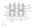

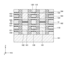
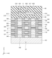
Priority Applications (1)
| Application Number | Priority Date | Filing Date | Title |
|---|---|---|---|
| JP2024118650A JP7704265B2 (ja) | 2020-05-14 | 2024-07-24 | 半導体装置及びその製造方法 |
Applications Claiming Priority (1)
| Application Number | Priority Date | Filing Date | Title |
|---|---|---|---|
| PCT/JP2020/019228 WO2021229740A1 (ja) | 2020-05-14 | 2020-05-14 | 半導体装置及びその製造方法 |
Related Child Applications (1)
| Application Number | Title | Priority Date | Filing Date |
|---|---|---|---|
| JP2024118650A Division JP7704265B2 (ja) | 2020-05-14 | 2024-07-24 | 半導体装置及びその製造方法 |
Publications (3)
| Publication Number | Publication Date |
|---|---|
| JPWO2021229740A1 JPWO2021229740A1 (https=) | 2021-11-18 |
| JPWO2021229740A5 true JPWO2021229740A5 (https=) | 2023-06-05 |
| JP7533575B2 JP7533575B2 (ja) | 2024-08-14 |
Family
ID=78525494
Family Applications (2)
| Application Number | Title | Priority Date | Filing Date |
|---|---|---|---|
| JP2022522426A Active JP7533575B2 (ja) | 2020-05-14 | 2020-05-14 | 半導体装置及びその製造方法 |
| JP2024118650A Active JP7704265B2 (ja) | 2020-05-14 | 2024-07-24 | 半導体装置及びその製造方法 |
Family Applications After (1)
| Application Number | Title | Priority Date | Filing Date |
|---|---|---|---|
| JP2024118650A Active JP7704265B2 (ja) | 2020-05-14 | 2024-07-24 | 半導体装置及びその製造方法 |
Country Status (4)
| Country | Link |
|---|---|
| US (2) | US12543353B2 (https=) |
| JP (2) | JP7533575B2 (https=) |
| CN (1) | CN115552604A (https=) |
| WO (1) | WO2021229740A1 (https=) |
Families Citing this family (13)
| Publication number | Priority date | Publication date | Assignee | Title |
|---|---|---|---|---|
| JP7302658B2 (ja) * | 2019-06-18 | 2023-07-04 | 株式会社ソシオネクスト | 半導体装置 |
| JP7640861B2 (ja) * | 2019-10-18 | 2025-03-06 | 株式会社ソシオネクスト | 半導体集積回路装置 |
| US20220359545A1 (en) * | 2021-05-07 | 2022-11-10 | Taiwan Semiconductor Manufacturing Company, Ltd. | Semiconductor memory devices with dielectric fin structures |
| EP4199052B1 (en) * | 2021-12-17 | 2024-08-21 | IMEC vzw | Metallization scheme for an integrated circuit |
| US12527078B2 (en) | 2021-12-21 | 2026-01-13 | Intel Corporation | Gate-all-around integrated circuit structures having epitaxial source or drain region lateral isolation |
| US12310064B2 (en) * | 2022-07-29 | 2025-05-20 | International Business Machines Corporation | Isolation pillar structures for stacked device structures |
| US20240105727A1 (en) * | 2022-09-23 | 2024-03-28 | Apple Inc. | Vertical Transistor Cell Structures Utilizing Topside and Backside Resources |
| US20250006730A1 (en) * | 2023-06-27 | 2025-01-02 | International Business Machines Corporation | Stacked transistors with dielectric insulator layers |
| US20250048677A1 (en) * | 2023-08-02 | 2025-02-06 | International Business Machines Corporation | Backside power rail to backside contact connection |
| EP4539635A1 (en) * | 2023-10-13 | 2025-04-16 | Samsung Electronics Co., Ltd | Semiconductor device, array structure including the semiconductor device, and method of manufacturing the semiconductor device |
| US20250185356A1 (en) * | 2023-12-05 | 2025-06-05 | International Business Machines Corporation | Self-aligned backside gate cut dielectric with air gap |
| US20250254988A1 (en) * | 2024-02-05 | 2025-08-07 | Samsung Electronics Co., Ltd. | Semiconductor device including stacked forksheet transistor structure with isolation wall |
| WO2025211200A1 (ja) * | 2024-04-01 | 2025-10-09 | 株式会社ソシオネクスト | 半導体集積回路装置 |
Family Cites Families (25)
| Publication number | Priority date | Publication date | Assignee | Title |
|---|---|---|---|---|
| JP2001358319A (ja) * | 2000-06-12 | 2001-12-26 | Mitsubishi Electric Corp | 交差ゲート構造を持つ半導体装置およびその製造方法 |
| US8753942B2 (en) | 2010-12-01 | 2014-06-17 | Intel Corporation | Silicon and silicon germanium nanowire structures |
| WO2013095341A1 (en) * | 2011-12-19 | 2013-06-27 | Intel Corporation | Cmos implementation of germanium and iii-v nanowires and nanoribbons in gate-all-around architecture |
| EP3127862B1 (en) | 2015-08-06 | 2018-04-18 | IMEC vzw | A method of manufacturing a gate-all-around nanowire device comprising two different nanowires |
| US9570395B1 (en) | 2015-11-17 | 2017-02-14 | Samsung Electronics Co., Ltd. | Semiconductor device having buried power rail |
| TWI739879B (zh) * | 2016-08-10 | 2021-09-21 | 日商東京威力科創股份有限公司 | 用於半導體裝置的延伸區域 |
| US9837414B1 (en) * | 2016-10-31 | 2017-12-05 | International Business Machines Corporation | Stacked complementary FETs featuring vertically stacked horizontal nanowires |
| US10586765B2 (en) | 2017-06-22 | 2020-03-10 | Tokyo Electron Limited | Buried power rails |
| US10546925B2 (en) * | 2017-11-02 | 2020-01-28 | International Business Machines Corporation | Vertically stacked nFET and pFET with dual work function |
| US10236217B1 (en) * | 2017-11-02 | 2019-03-19 | International Business Machines Corporation | Stacked field-effect transistors (FETs) with shared and non-shared gates |
| US10833078B2 (en) * | 2017-12-04 | 2020-11-10 | Tokyo Electron Limited | Semiconductor apparatus having stacked gates and method of manufacture thereof |
| US10566438B2 (en) * | 2018-04-02 | 2020-02-18 | International Business Machines Corporation | Nanosheet transistor with dual inner airgap spacers |
| US10424639B1 (en) * | 2018-04-19 | 2019-09-24 | International Business Machines Corporation | Nanosheet transistor with high-mobility channel |
| US11201152B2 (en) * | 2018-04-20 | 2021-12-14 | Globalfoundries Inc. | Method, apparatus, and system for fin-over-nanosheet complementary field-effect-transistor |
| US10490667B1 (en) * | 2018-05-15 | 2019-11-26 | International Business Machines Corporation | Three-dimensional field effect device |
| US10707218B2 (en) * | 2018-07-26 | 2020-07-07 | Globalfoundries Inc. | Two port SRAM cell using complementary nano-sheet/wire transistor devices |
| US10510620B1 (en) * | 2018-07-27 | 2019-12-17 | GlobalFoundries, Inc. | Work function metal patterning for N-P space between active nanostructures |
| US10559566B1 (en) * | 2018-09-17 | 2020-02-11 | International Business Machines Corporation | Reduction of multi-threshold voltage patterning damage in nanosheet device structure |
| JP7351307B2 (ja) | 2018-09-25 | 2023-09-27 | 株式会社ソシオネクスト | 半導体装置及びその製造方法 |
| US10741456B2 (en) * | 2018-10-10 | 2020-08-11 | International Business Machines Corporation | Vertically stacked nanosheet CMOS transistor |
| US10734447B2 (en) * | 2018-10-22 | 2020-08-04 | International Business Machines Corporation | Field-effect transistor unit cells for neural networks with differential weights |
| US10818674B2 (en) * | 2019-03-07 | 2020-10-27 | Globalfoundries Inc. | Structures and SRAM bit cells integrating complementary field-effect transistors |
| WO2021138551A1 (en) * | 2019-12-31 | 2021-07-08 | Tokyo Electron Limited | Cfet sram bit cell with three stacked device decks |
| US11239236B2 (en) | 2020-03-23 | 2022-02-01 | Intel Corporation | Forksheet transistor architectures |
| US11626494B2 (en) * | 2020-06-17 | 2023-04-11 | Taiwan Semiconductor Manufacturing Co., Ltd. | Epitaxial backside contact |
-
2020
- 2020-05-14 CN CN202080100676.1A patent/CN115552604A/zh active Pending
- 2020-05-14 WO PCT/JP2020/019228 patent/WO2021229740A1/ja not_active Ceased
- 2020-05-14 JP JP2022522426A patent/JP7533575B2/ja active Active
-
2022
- 2022-11-07 US US17/982,005 patent/US12543353B2/en active Active
-
2024
- 2024-07-24 JP JP2024118650A patent/JP7704265B2/ja active Active
-
2025
- 2025-12-03 US US19/407,255 patent/US20260090041A1/en active Pending
Similar Documents
| Publication | Publication Date | Title |
|---|---|---|
| JPWO2021229740A5 (https=) | ||
| JP2017034246A5 (ja) | 半導体装置の作製方法 | |
| JP2021082496A5 (https=) | ||
| JP2015188079A5 (https=) | ||
| JP2020516089A5 (https=) | ||
| WO2015119893A3 (en) | Method of fabricating a charge-trapping gate stack using a cmos process flow | |
| JP2012516036A5 (https=) | ||
| JP2017191934A5 (https=) | ||
| KR20180084588A (ko) | 반도체 패키지의 제조 방법 | |
| JP2010262977A5 (https=) | ||
| JP2011060901A5 (https=) | ||
| CN114424334A (zh) | 一种芯片封装结构、方法及芯片模组 | |
| JP1737181S (ja) | 半導体処理装置用シャワーヘッド | |
| JP2012023350A5 (https=) | ||
| IL287669A (en) | Metal removal method, dry etching method, and production method for semiconductor element | |
| JP2014157893A5 (https=) | ||
| IL302057A (en) | Etching gas, etching method, and method for producing semiconductor element | |
| JP2021111676A5 (https=) | ||
| CN109411338A (zh) | 制造半导体元件的方法 | |
| CN102437064B (zh) | 硅纳米线的制造方法 | |
| JP2024058234A5 (https=) | ||
| JP2017044892A5 (https=) | ||
| JPWO2022030461A5 (https=) | ||
| JPWO2020013305A5 (https=) | ||
| JP1733645S (ja) | 半導体処理装置用シャワーヘッド |