JPWO2005073740A1 - 試験装置及び試験方法 - Google Patents
試験装置及び試験方法 Download PDFInfo
- Publication number
- JPWO2005073740A1 JPWO2005073740A1 JP2005517453A JP2005517453A JPWO2005073740A1 JP WO2005073740 A1 JPWO2005073740 A1 JP WO2005073740A1 JP 2005517453 A JP2005517453 A JP 2005517453A JP 2005517453 A JP2005517453 A JP 2005517453A JP WO2005073740 A1 JPWO2005073740 A1 JP WO2005073740A1
- Authority
- JP
- Japan
- Prior art keywords
- signal
- test
- circuit
- result
- relay
- Prior art date
- Legal status (The legal status is an assumption and is not a legal conclusion. Google has not performed a legal analysis and makes no representation as to the accuracy of the status listed.)
- Granted
Links
- 238000012360 testing method Methods 0.000 title claims abstract description 314
- 238000010998 test method Methods 0.000 title claims description 11
- 230000005540 biological transmission Effects 0.000 claims abstract description 64
- 230000004044 response Effects 0.000 claims abstract description 4
- 230000008054 signal transmission Effects 0.000 claims description 13
- 230000007274 generation of a signal involved in cell-cell signaling Effects 0.000 description 19
- 238000007493 shaping process Methods 0.000 description 18
- 238000000034 method Methods 0.000 description 10
- 239000004065 semiconductor Substances 0.000 description 9
- 238000010586 diagram Methods 0.000 description 6
- 230000001419 dependent effect Effects 0.000 description 1
- 230000006870 function Effects 0.000 description 1
- 238000010348 incorporation Methods 0.000 description 1
- 238000012986 modification Methods 0.000 description 1
- 230000004048 modification Effects 0.000 description 1
Images
Classifications
-
- G—PHYSICS
- G01—MEASURING; TESTING
- G01R—MEASURING ELECTRIC VARIABLES; MEASURING MAGNETIC VARIABLES
- G01R31/00—Arrangements for testing electric properties; Arrangements for locating electric faults; Arrangements for electrical testing characterised by what is being tested not provided for elsewhere
- G01R31/28—Testing of electronic circuits, e.g. by signal tracer
- G01R31/317—Testing of digital circuits
- G01R31/3181—Functional testing
- G01R31/319—Tester hardware, i.e. output processing circuits
- G01R31/3193—Tester hardware, i.e. output processing circuits with comparison between actual response and known fault free response
- G01R31/31932—Comparators
-
- G—PHYSICS
- G01—MEASURING; TESTING
- G01R—MEASURING ELECTRIC VARIABLES; MEASURING MAGNETIC VARIABLES
- G01R31/00—Arrangements for testing electric properties; Arrangements for locating electric faults; Arrangements for electrical testing characterised by what is being tested not provided for elsewhere
- G01R31/28—Testing of electronic circuits, e.g. by signal tracer
- G01R31/317—Testing of digital circuits
- G01R31/3181—Functional testing
- G01R31/319—Tester hardware, i.e. output processing circuits
- G01R31/31917—Stimuli generation or application of test patterns to the device under test [DUT]
- G01R31/31924—Voltage or current aspects, e.g. driver, receiver
Landscapes
- Engineering & Computer Science (AREA)
- General Engineering & Computer Science (AREA)
- Physics & Mathematics (AREA)
- General Physics & Mathematics (AREA)
- Tests Of Electronic Circuits (AREA)
Abstract
Description
文献の参照による組み込みが認められる指定国については、下記の出願に記載された内容を参照により本出願に組み込み、本出願の記載の一部とする。
特願2004−021851 出願日 平成16年1月29日
試験信号はデジタル信号であり、当該試験装置は、設定電圧出力部における予め定められた設定電圧を、H論理又はL論理に切り替え可能に設定する電圧設定部を更に備えてもよい。
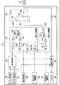
また、本実施形態に係る試験装置10によれば、DUT15に対する試験信号の書込動作と、DUT15からの結果信号の読込動作とを切り替える場合に、リレーを用いるか否かを制御できる。これにより、利用者の要望に応じて試験方法を適切に切り替えることができる。
一方、試験装置10がDUT15に対して読込動作を行う場合(S1040:Yes)、設定電圧出力部110は、試験信号の電圧を予め定められた電圧値に設定して、ドライバ122に出力する(S1070)。そして、ドライバ122は、電圧が予め定められた電圧値に設定された試験信号を出力することにより、結果信号の伝送路を終端する(S1080)。続いて、コンパレータ128は、DUT15が出力した結果信号を予め定められた基準電圧と比較し、比較結果を論理比較部130に出力する(S1090)。続いて、論理比較部130は、コンパレータ128から受け取った比較結果に基づいてDUT15の良否を判定する(S1100)。
以上により、試験装置10は、区間200において、第1リレー120を短絡すると共に第2リレー124を開放することにより、DUT15に試験信号を印加する。
以上により、試験装置10は、区間210において、ドライバ122に常にL論理を示す信号を出力し、更に、第1リレー120を短絡すると共に第2リレー124を開放することにより、ドライバ122を用いて結果信号の伝送路を終端する。
以上により、試験装置10は、区間220において、第1リレー120を短絡すると共に第2リレー124を開放することにより、DUT15に試験信号を印加する。
以上により、試験装置10は、区間230において、第1リレー120を開放すると共に第2リレー124を短絡することにより、終端回路126を用いて結果信号の伝送路を終端する。
また、本実施形態に係る試験装置10によれば、DUT15に対する試験信号の書込動作とDUT15からの結果信号の読込動作とを切り替える場合にリレーを用いるか否かを、リレー制御信号に基づいて制御できる。これにより、DUT15の特性に応じた試験方法を適切に選択することができるので、効率よく試験を行うことができる。
以上により、試験装置30は、区間400において、第1リレー120を短絡すると共に第2リレー124を開放することにより、DUT15に試験信号を印加する。
以上により、試験装置30は、区間410において、ドライバ122に常にH論理を示す信号を出力し、更に第1リレー120を短絡すると共に第2リレー124を開放することにより、ドライバ122を用いて結果信号の伝送路を終端する。
以上により、試験装置30は、区間420において、第1リレー120を短絡すると共に第2リレー124を開放することにより、DUT15に試験信号を印加する。
以上により、試験装置30は、区間430において、ドライバ122に常にL論理を示す信号を出力し、更に第1リレー120を短絡すると共に第2リレー124を開放することにより、ドライバ122を用いて結果信号の伝送路を終端する。
本実施形態に係る試験装置50は、結果信号の伝送路をドライバ560により終端させる場合に、試験信号に基づいて決定した電圧を用いるのか、終端電圧VTを用いるのかを切替可能に制御することを目的とする。
以上により、第2リレー制御部540は、試験装置50がDUT55に対して書込動作を行う場合にはH論理を、読込動作を行う場合には終端方法制御信号が示す論理値をドライバ560に出力する。
Claims (7)
- 前記被試験デバイスを試験する試験装置であって、
前記被試験デバイスに試験信号を印加するドライバと、
印加された前記試験信号に対応して前記被試験デバイスが出力した結果信号を、予め定められた基準電圧と比較するコンパレータと、
前記被試験デバイスに対して読込動作を行う場合に、前記試験信号の電圧を予め定められた電圧値に設定することにより、前記結果信号の伝送路を前記ドライバに終端させる設定電圧出力部と
を備える試験装置。 - 前記試験信号はデジタル信号であり、
当該試験装置は、
前記設定電圧出力部における予め定められた設定電圧を、H論理又はL論理に切り替え可能に設定する電圧設定部
を更に備える請求項1記載の試験装置。 - 前記ドライバに前記試験信号を供給するか否かを切り替える第1リレーと、
前記結果信号の伝送路を終端する終端回路と、
前記結果信号の伝送路を前記終端回路に終端させるか否かを切り替える第2リレーと、
前記被試験デバイスに対して読込動作を行う場合に、前記設定電圧出力部が前記結果信号の伝送路を前記ドライバに終端させるのに代えて、前記第1リレーが前記ドライバへの前記試験信号の供給を停止すると共に前記第2リレーが前記結果信号の伝送路を前記終端回路に終端させるか否かを、切り替え可能に制御するリレー制御部と
を更に備える請求項1記載の試験装置。 - 前記試験信号はデジタル信号であり、
当該試験装置は、
前記被試験デバイスに対して書込動作を行う場合にはH論理を、読込動作を行う場合にはL論理を示す動作制御信号を生成する動作制御部
を更に備え、
前記設定電圧出力部は、
前記試験信号と前記動作制御信号との論理積演算を行い、当該演算の結果を前記ドライバに出力することにより、前記被試験デバイスに対して読込動作を行う場合に、前記試験信号の電圧値をL論理に設定して前記結果信号の伝送路を前記ドライバに終端させる論理積回路
を有する請求項1記載の試験装置。 - 前記被試験デバイスに対して書込動作を行う場合にはH論理を、読込動作を行う場合にはL論理を示す動作制御信号を生成する動作制御部
を更に備え、
前記電圧設定部は、
前記設定電圧出力部における予め定められた前記設定電圧を示す電圧設定制御信号を生成する電圧設定制御部と、
前記動作制御信号の反転値と前記電圧設定制御信号の反転値との論理積演算を行い、当該演算の結果の反転値を出力する第1論理積回路と、
前記動作制御信号の反転値と前記電圧設定制御信号との論理積演算を行う第2論理積回路と
を有し、
前記設定電圧出力部は、
前記試験信号と前記第1論理積回路が出力する演算結果の反転値との論理積演算を行う第3論理積回路と、
前記第3論理積回路の演算結果と前記第2論理積回路の演算結果との論理和演算を行い、当該演算の結果を前記ドライバに出力することにより、前記被試験デバイスに対して読込動作を行う場合に、前記試験信号の電圧値を前記電圧設定制御信号が示す値に設定し、前記結果信号の伝送路を前記ドライバに終端させる論理和回路と
を有する請求項2記載の試験装置。 - 前記試験信号はデジタル信号であり、
当該試験装置は、
前記被試験デバイスに対して書込動作を行う場合にはH論理を、読込動作を行う場合にはL論理を示す動作制御信号を生成する動作制御部
を更に備え、
前記リレー制御部は、
前記被試験デバイスに対する読込動作において、前記設定電圧出力部が前記結果信号の伝送路を前記ドライバに終端させる場合にはH論理を、前記第1リレーが前記ドライバへの前記試験信号の供給を停止すると共に、前記第2リレーが前記結果信号の伝送路を前記終端回路に終端させる場合にはL論理を示すリレー制御信号を生成するリレー制御信号生成部と、
前記動作制御信号の反転値と前記リレー制御信号との論理積演算を行い、当該演算の結果の反転値を出力する第1論理積回路と、
前記動作制御信号の反転値と前記リレー制御信号の反転値との論理積演算を行い、当該演算の結果の反転値を前記第1リレーの動作信号として出力すると共に当該演算の結果を前記第2リレーの動作信号として出力することにより、前記被試験デバイスに対して読込動作を行い、且つ前記リレー制御信号がL論理を示す場合に、前記ドライバへの前記試験信号の供給を停止し、前記結果信号の伝送路を前記終端回路に終端させる第2論理積回路と
を有し、
前記設定電圧出力部は、
前記試験信号と前記第1論理積回路が出力した演算結果の反転値との論理積演算を行い、当該演算の結果を前記第1リレーを経由して前記ドライバに出力することにより、前記被試験デバイスに対して読込動作を行い、且つ前記リレー制御信号がH論理を示す場合に、前記結果信号の伝送路を前記ドライバに終端させる第3論理積回路
を有する請求項3記載の試験装置。 - 被試験デバイスに試験信号を印加するドライバと、印加された前記試験信号に対応して前記被試験デバイスが出力した結果信号を、予め定められた基準電圧と比較するコンパレータとを備える試験装置において、前記被試験デバイスを試験する試験方法であって、
前記被試験デバイスに対して読込動作を行う場合に、前記試験信号の電圧を予め定められた電圧値に設定することにより、前記結果信号の伝送路を前記ドライバに終端させる設定電圧出力段階
を備える試験方法。
Applications Claiming Priority (3)
| Application Number | Priority Date | Filing Date | Title |
|---|---|---|---|
| JP2004021851 | 2004-01-29 | ||
| JP2004021851 | 2004-01-29 | ||
| PCT/JP2005/000993 WO2005073740A1 (ja) | 2004-01-29 | 2005-01-26 | 試験装置及び試験方法 |
Publications (2)
| Publication Number | Publication Date |
|---|---|
| JPWO2005073740A1 true JPWO2005073740A1 (ja) | 2007-09-13 |
| JP4473821B2 JP4473821B2 (ja) | 2010-06-02 |
Family
ID=34823811
Family Applications (1)
| Application Number | Title | Priority Date | Filing Date |
|---|---|---|---|
| JP2005517453A Expired - Fee Related JP4473821B2 (ja) | 2004-01-29 | 2005-01-26 | 試験装置及び試験方法 |
Country Status (4)
| Country | Link |
|---|---|
| US (1) | US7409615B2 (ja) |
| JP (1) | JP4473821B2 (ja) |
| DE (1) | DE112005000268T5 (ja) |
| WO (1) | WO2005073740A1 (ja) |
Families Citing this family (6)
| Publication number | Priority date | Publication date | Assignee | Title |
|---|---|---|---|---|
| JP2007010606A (ja) * | 2005-07-04 | 2007-01-18 | Matsushita Electric Ind Co Ltd | Lsi検査モジュール、lsi検査モジュールの制御方法、lsi検査モジュールとlsi検査装置との通信方法、およびlsi検査方法 |
| US7755377B2 (en) * | 2007-11-16 | 2010-07-13 | Advantest Corporation | Driver circuit and test apparatus |
| US7589549B2 (en) * | 2007-11-16 | 2009-09-15 | Advantest Corporation | Driver circuit and test apparatus |
| US7962110B2 (en) * | 2008-02-14 | 2011-06-14 | Advantest Corporation | Driver circuit and test apparatus |
| US8516410B2 (en) * | 2008-12-30 | 2013-08-20 | International Business Machines Corporation | Method of migrating electronic devices operating in current mode to a target technology |
| JP2022115179A (ja) * | 2021-01-28 | 2022-08-09 | キオクシア株式会社 | 半導体集積回路装置及びその動作方法 |
Family Cites Families (6)
| Publication number | Priority date | Publication date | Assignee | Title |
|---|---|---|---|---|
| US6445208B1 (en) * | 2000-04-06 | 2002-09-03 | Advantest Corp. | Power source current measurement unit for semiconductor test system |
| JP2002139551A (ja) * | 2000-11-02 | 2002-05-17 | Advantest Corp | 半導体試験装置 |
| JP4149273B2 (ja) * | 2002-01-18 | 2008-09-10 | 株式会社日立製作所 | パルス発生回路およびパルス発生回路を用いた半導体試験装置、および半導体試験方法および半導体装置の製造方法 |
| US6762614B2 (en) * | 2002-04-18 | 2004-07-13 | Agilent Technologies, Inc. | Systems and methods for facilitating driver strength testing of integrated circuits |
| WO2004104605A1 (ja) * | 2003-05-21 | 2004-12-02 | Advantest Corporation | 電流測定装置及び試験装置 |
| US7023233B1 (en) * | 2004-10-12 | 2006-04-04 | Advantest Corporation | Test apparatus and test method |
-
2005
- 2005-01-26 JP JP2005517453A patent/JP4473821B2/ja not_active Expired - Fee Related
- 2005-01-26 WO PCT/JP2005/000993 patent/WO2005073740A1/ja not_active Ceased
- 2005-01-26 DE DE112005000268T patent/DE112005000268T5/de not_active Withdrawn
-
2006
- 2006-07-28 US US11/495,186 patent/US7409615B2/en not_active Expired - Fee Related
Also Published As
| Publication number | Publication date |
|---|---|
| US20070022346A1 (en) | 2007-01-25 |
| WO2005073740A1 (ja) | 2005-08-11 |
| US7409615B2 (en) | 2008-08-05 |
| DE112005000268T5 (de) | 2007-02-01 |
| JP4473821B2 (ja) | 2010-06-02 |
Similar Documents
| Publication | Publication Date | Title |
|---|---|---|
| TW488007B (en) | Glitch detection for semiconductor test system | |
| US7373574B2 (en) | Semiconductor testing apparatus and method of testing semiconductor | |
| JPH07110357A (ja) | 半導体ic試験装置 | |
| JP4473821B2 (ja) | 試験装置及び試験方法 | |
| CN101646954A (zh) | 测试装置及电子器件 | |
| TW459141B (en) | Driver with transmission path loss compensation | |
| KR100545440B1 (ko) | 반도체 시험장치 | |
| JPH06194414A (ja) | Ic機能試験装置及び試験方法 | |
| US7202688B2 (en) | Output buffer circuit having signal path used for testing and integrated circuit and test method including the same | |
| US5732047A (en) | Timing comparator circuit for use in device testing apparatus | |
| US6064242A (en) | I/O pin electronics circuit having a pair of drivers | |
| JP2006012253A (ja) | 試験装置及び試験方法 | |
| JP3375597B2 (ja) | 差分信号の交差電圧をテストするための装置及びその方法 | |
| WO2002050557A1 (fr) | Calculateur de duree de gigue et testeur | |
| JPS6329277A (ja) | 論理集積回路の試験装置 | |
| JPH1010200A (ja) | 半導体装置の試験方法及び半導体試験装置 | |
| JPH0559354U (ja) | Ic試験装置 | |
| JPH04259868A (ja) | Ic試験装置 | |
| JP4333527B2 (ja) | Icテスタ | |
| JP3186555B2 (ja) | 集積回路装置と基板との接続テスト装置および接続テスト方法 | |
| JPWO2012004833A1 (ja) | 試験装置 | |
| JPH10253707A (ja) | 集積回路試験装置 | |
| JP4670783B2 (ja) | 半導体試験装置 | |
| JP2001228214A (ja) | 半導体試験装置 | |
| JPH10339768A (ja) | 半導体試験装置のテストプログラム実行方法 |
Legal Events
| Date | Code | Title | Description |
|---|---|---|---|
| A621 | Written request for application examination |
Free format text: JAPANESE INTERMEDIATE CODE: A621 Effective date: 20070920 |
|
| A621 | Written request for application examination |
Free format text: JAPANESE INTERMEDIATE CODE: A621 Effective date: 20070920 |
|
| A131 | Notification of reasons for refusal |
Free format text: JAPANESE INTERMEDIATE CODE: A131 Effective date: 20100105 |
|
| A521 | Request for written amendment filed |
Free format text: JAPANESE INTERMEDIATE CODE: A523 Effective date: 20100127 |
|
| TRDD | Decision of grant or rejection written | ||
| A01 | Written decision to grant a patent or to grant a registration (utility model) |
Free format text: JAPANESE INTERMEDIATE CODE: A01 Effective date: 20100302 |
|
| A01 | Written decision to grant a patent or to grant a registration (utility model) |
Free format text: JAPANESE INTERMEDIATE CODE: A01 |
|
| A61 | First payment of annual fees (during grant procedure) |
Free format text: JAPANESE INTERMEDIATE CODE: A61 Effective date: 20100305 |
|
| FPAY | Renewal fee payment (event date is renewal date of database) |
Free format text: PAYMENT UNTIL: 20130312 Year of fee payment: 3 |
|
| R150 | Certificate of patent or registration of utility model |
Ref document number: 4473821 Country of ref document: JP Free format text: JAPANESE INTERMEDIATE CODE: R150 |
|
| FPAY | Renewal fee payment (event date is renewal date of database) |
Free format text: PAYMENT UNTIL: 20130312 Year of fee payment: 3 |
|
| FPAY | Renewal fee payment (event date is renewal date of database) |
Free format text: PAYMENT UNTIL: 20130312 Year of fee payment: 3 |
|
| FPAY | Renewal fee payment (event date is renewal date of database) |
Free format text: PAYMENT UNTIL: 20140312 Year of fee payment: 4 |
|
| R250 | Receipt of annual fees |
Free format text: JAPANESE INTERMEDIATE CODE: R250 |
|
| R250 | Receipt of annual fees |
Free format text: JAPANESE INTERMEDIATE CODE: R250 |
|
| R250 | Receipt of annual fees |
Free format text: JAPANESE INTERMEDIATE CODE: R250 |
|
| R250 | Receipt of annual fees |
Free format text: JAPANESE INTERMEDIATE CODE: R250 |
|
| R250 | Receipt of annual fees |
Free format text: JAPANESE INTERMEDIATE CODE: R250 |
|
| R250 | Receipt of annual fees |
Free format text: JAPANESE INTERMEDIATE CODE: R250 |
|
| R250 | Receipt of annual fees |
Free format text: JAPANESE INTERMEDIATE CODE: R250 |
|
| R250 | Receipt of annual fees |
Free format text: JAPANESE INTERMEDIATE CODE: R250 |
|
| R250 | Receipt of annual fees |
Free format text: JAPANESE INTERMEDIATE CODE: R250 |
|
| R250 | Receipt of annual fees |
Free format text: JAPANESE INTERMEDIATE CODE: R250 |
|
| R250 | Receipt of annual fees |
Free format text: JAPANESE INTERMEDIATE CODE: R250 |
|
| LAPS | Cancellation because of no payment of annual fees |