JP7697286B2 - 炭化珪素半導体装置および炭化珪素半導体装置の製造方法 - Google Patents
炭化珪素半導体装置および炭化珪素半導体装置の製造方法 Download PDFInfo
- Publication number
- JP7697286B2 JP7697286B2 JP2021102718A JP2021102718A JP7697286B2 JP 7697286 B2 JP7697286 B2 JP 7697286B2 JP 2021102718 A JP2021102718 A JP 2021102718A JP 2021102718 A JP2021102718 A JP 2021102718A JP 7697286 B2 JP7697286 B2 JP 7697286B2
- Authority
- JP
- Japan
- Prior art keywords
- trench
- film
- insulating film
- gate insulating
- gate
- Prior art date
- Legal status (The legal status is an assumption and is not a legal conclusion. Google has not performed a legal analysis and makes no representation as to the accuracy of the status listed.)
- Active
Links
Images


Classifications
-
- H—ELECTRICITY
- H01—ELECTRIC ELEMENTS
- H01L—SEMICONDUCTOR DEVICES NOT COVERED BY CLASS H10
- H01L21/00—Processes or apparatus adapted for the manufacture or treatment of semiconductor or solid state devices or of parts thereof
- H01L21/02—Manufacture or treatment of semiconductor devices or of parts thereof
- H01L21/04—Manufacture or treatment of semiconductor devices or of parts thereof the devices having potential barriers, e.g. a PN junction, depletion layer or carrier concentration layer
- H01L21/0445—Manufacture or treatment of semiconductor devices or of parts thereof the devices having potential barriers, e.g. a PN junction, depletion layer or carrier concentration layer the devices having semiconductor bodies comprising crystalline silicon carbide
- H01L21/048—Making electrodes
- H01L21/049—Conductor-insulator-semiconductor electrodes, e.g. MIS contacts
-
- H—ELECTRICITY
- H10—SEMICONDUCTOR DEVICES; ELECTRIC SOLID-STATE DEVICES NOT OTHERWISE PROVIDED FOR
- H10D—INORGANIC ELECTRIC SEMICONDUCTOR DEVICES
- H10D12/00—Bipolar devices controlled by the field effect, e.g. insulated-gate bipolar transistors [IGBT]
- H10D12/01—Manufacture or treatment
- H10D12/031—Manufacture or treatment of IGBTs
- H10D12/032—Manufacture or treatment of IGBTs of vertical IGBTs
- H10D12/038—Manufacture or treatment of IGBTs of vertical IGBTs having a recessed gate, e.g. trench-gate IGBTs
-
- H—ELECTRICITY
- H10—SEMICONDUCTOR DEVICES; ELECTRIC SOLID-STATE DEVICES NOT OTHERWISE PROVIDED FOR
- H10D—INORGANIC ELECTRIC SEMICONDUCTOR DEVICES
- H10D30/00—Field-effect transistors [FET]
- H10D30/01—Manufacture or treatment
- H10D30/021—Manufacture or treatment of FETs having insulated gates [IGFET]
- H10D30/028—Manufacture or treatment of FETs having insulated gates [IGFET] of double-diffused metal oxide semiconductor [DMOS] FETs
- H10D30/0291—Manufacture or treatment of FETs having insulated gates [IGFET] of double-diffused metal oxide semiconductor [DMOS] FETs of vertical DMOS [VDMOS] FETs
- H10D30/0297—Manufacture or treatment of FETs having insulated gates [IGFET] of double-diffused metal oxide semiconductor [DMOS] FETs of vertical DMOS [VDMOS] FETs using recessing of the gate electrodes, e.g. to form trench gate electrodes
-
- H—ELECTRICITY
- H10—SEMICONDUCTOR DEVICES; ELECTRIC SOLID-STATE DEVICES NOT OTHERWISE PROVIDED FOR
- H10D—INORGANIC ELECTRIC SEMICONDUCTOR DEVICES
- H10D30/00—Field-effect transistors [FET]
- H10D30/60—Insulated-gate field-effect transistors [IGFET]
- H10D30/64—Double-diffused metal-oxide semiconductor [DMOS] FETs
- H10D30/66—Vertical DMOS [VDMOS] FETs
- H10D30/668—Vertical DMOS [VDMOS] FETs having trench gate electrodes, e.g. UMOS transistors
-
- H—ELECTRICITY
- H10—SEMICONDUCTOR DEVICES; ELECTRIC SOLID-STATE DEVICES NOT OTHERWISE PROVIDED FOR
- H10D—INORGANIC ELECTRIC SEMICONDUCTOR DEVICES
- H10D62/00—Semiconductor bodies, or regions thereof, of devices having potential barriers
- H10D62/10—Shapes, relative sizes or dispositions of the regions of the semiconductor bodies; Shapes of the semiconductor bodies
- H10D62/102—Constructional design considerations for preventing surface leakage or controlling electric field concentration
- H10D62/103—Constructional design considerations for preventing surface leakage or controlling electric field concentration for increasing or controlling the breakdown voltage of reverse-biased devices
- H10D62/105—Constructional design considerations for preventing surface leakage or controlling electric field concentration for increasing or controlling the breakdown voltage of reverse-biased devices by having particular doping profiles, shapes or arrangements of PN junctions; by having supplementary regions, e.g. junction termination extension [JTE]
- H10D62/106—Constructional design considerations for preventing surface leakage or controlling electric field concentration for increasing or controlling the breakdown voltage of reverse-biased devices by having particular doping profiles, shapes or arrangements of PN junctions; by having supplementary regions, e.g. junction termination extension [JTE] having supplementary regions doped oppositely to or in rectifying contact with regions of the semiconductor bodies, e.g. guard rings with PN or Schottky junctions
- H10D62/107—Buried supplementary regions, e.g. buried guard rings
-
- H—ELECTRICITY
- H10—SEMICONDUCTOR DEVICES; ELECTRIC SOLID-STATE DEVICES NOT OTHERWISE PROVIDED FOR
- H10D—INORGANIC ELECTRIC SEMICONDUCTOR DEVICES
- H10D62/00—Semiconductor bodies, or regions thereof, of devices having potential barriers
- H10D62/10—Shapes, relative sizes or dispositions of the regions of the semiconductor bodies; Shapes of the semiconductor bodies
- H10D62/13—Semiconductor regions connected to electrodes carrying current to be rectified, amplified or switched, e.g. source or drain regions
- H10D62/149—Source or drain regions of field-effect devices
- H10D62/151—Source or drain regions of field-effect devices of IGFETs
- H10D62/156—Drain regions of DMOS transistors
- H10D62/157—Impurity concentrations or distributions
-
- H—ELECTRICITY
- H10—SEMICONDUCTOR DEVICES; ELECTRIC SOLID-STATE DEVICES NOT OTHERWISE PROVIDED FOR
- H10D—INORGANIC ELECTRIC SEMICONDUCTOR DEVICES
- H10D62/00—Semiconductor bodies, or regions thereof, of devices having potential barriers
- H10D62/10—Shapes, relative sizes or dispositions of the regions of the semiconductor bodies; Shapes of the semiconductor bodies
- H10D62/17—Semiconductor regions connected to electrodes not carrying current to be rectified, amplified or switched, e.g. channel regions
- H10D62/393—Body regions of DMOS transistors or IGBTs
-
- H—ELECTRICITY
- H10—SEMICONDUCTOR DEVICES; ELECTRIC SOLID-STATE DEVICES NOT OTHERWISE PROVIDED FOR
- H10D—INORGANIC ELECTRIC SEMICONDUCTOR DEVICES
- H10D62/00—Semiconductor bodies, or regions thereof, of devices having potential barriers
- H10D62/80—Semiconductor bodies, or regions thereof, of devices having potential barriers characterised by the materials
- H10D62/83—Semiconductor bodies, or regions thereof, of devices having potential barriers characterised by the materials being Group IV materials, e.g. B-doped Si or undoped Ge
- H10D62/832—Semiconductor bodies, or regions thereof, of devices having potential barriers characterised by the materials being Group IV materials, e.g. B-doped Si or undoped Ge being Group IV materials comprising two or more elements, e.g. SiGe
- H10D62/8325—Silicon carbide
-
- H—ELECTRICITY
- H10—SEMICONDUCTOR DEVICES; ELECTRIC SOLID-STATE DEVICES NOT OTHERWISE PROVIDED FOR
- H10D—INORGANIC ELECTRIC SEMICONDUCTOR DEVICES
- H10D64/00—Electrodes of devices having potential barriers
- H10D64/20—Electrodes characterised by their shapes, relative sizes or dispositions
- H10D64/27—Electrodes not carrying the current to be rectified, amplified, oscillated or switched, e.g. gates
- H10D64/311—Gate electrodes for field-effect devices
- H10D64/411—Gate electrodes for field-effect devices for FETs
- H10D64/511—Gate electrodes for field-effect devices for FETs for IGFETs
- H10D64/514—Gate electrodes for field-effect devices for FETs for IGFETs characterised by the insulating layers
- H10D64/516—Gate electrodes for field-effect devices for FETs for IGFETs characterised by the insulating layers the thicknesses being non-uniform
Landscapes
- Engineering & Computer Science (AREA)
- Chemical & Material Sciences (AREA)
- Crystallography & Structural Chemistry (AREA)
- Physics & Mathematics (AREA)
- Condensed Matter Physics & Semiconductors (AREA)
- General Physics & Mathematics (AREA)
- Manufacturing & Machinery (AREA)
- Computer Hardware Design (AREA)
- Microelectronics & Electronic Packaging (AREA)
- Power Engineering (AREA)
- Formation Of Insulating Films (AREA)
- Electrodes Of Semiconductors (AREA)
Description
実施の形態にかかる炭化珪素半導体装置の構造について説明する。図1は、実施の形態にかかる炭化珪素半導体装置の構造を示す断面図である。図2は、図1のトレンチ付近を拡大して模式的に示す拡大図である。図1に示す実施の形態にかかる炭化珪素半導体装置10は、炭化珪素(SiC)を半導体材料として用いた半導体基板(半導体チップ)30のおもて面側にトレンチゲート構造を備えた縦型MOSFETである。半導体基板30は、SiCを半導体材料として用いたn+型出発基板31のおもて面上に、n-型ドリフト領域2およびp型ベース領域3となる各エピタキシャル層32,33を順に積層してなるエピタキシャル基板である。
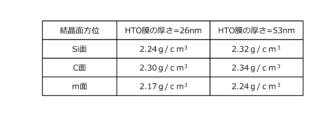
HTO膜(高温酸化により堆積したSiO2膜)の膜密度について検証した。図4は、実験例のHTO膜の厚さと膜密度との関係を示す図表である。図5は、実験例のHTO膜のSiC/SiO2界面からの距離と膜密度との関係を示す図表である。図4,5には、上述したステップS5(図3参照)のHTO堆積後アニールを行っていないHTO膜の膜密度のXRR法による測定値(測定誤差±0.03g/cm3)を示す。
上述した実施の形態にかかる炭化珪素半導体装置10の製造方法(図3参照)のステップS5のHTO堆積後アニール条件について検証した。図6は、HTO膜の膜密度とHTO堆積後アニール条件との関係を示す図表である。図7は、実施例のHTO膜中の酸素の二次イオン強度分布を示す特性図である。図8は、実施例のSiC/SiO2界面およびHTO膜中の窒素濃度分布を示す特性図である。
2 n-型ドリフト領域
3 p型ベース領域
4 n+型ソース領域
5 p++型コンタクト領域
6 トレンチ
7 ゲート絶縁膜(HTO膜)
7a ゲート絶縁膜の低密度膜
7b ゲート絶縁膜の高密度膜
8 ゲート電極
9 層間絶縁膜
10 炭化珪素半導体装置
11 ソース電極
12 ドレイン電極
20 トレンチの内壁とゲート絶縁膜との接合界面(SiC/SiO2界面)
21,22 p+型領域
23 n型電流拡散領域
30 半導体基板
31 n+型出発基板
32 n-型エピタキシャル層
33 p型エピタキシャル層
t1 ゲート絶縁膜(HTO膜)の厚さ
t11 ゲート絶縁膜の低密度膜の厚さ
Claims (8)
- ゲート-酸化膜-半導体の3層構造からなる絶縁ゲートを備えた炭化珪素半導体装置であって、
前記半導体を構成する、炭化珪素からなる半導体基板と、
前記半導体基板の第1主面から前記半導体基板の第1主面と直交する方向に延在する所定深さのトレンチと、
前記トレンチの内壁に沿って設けられ、前記トレンチの内壁で前記半導体基板に接する、前記酸化膜を構成するゲート絶縁膜と、
前記トレンチの内部において前記ゲート絶縁膜の上に設けられた、前記ゲートを構成するゲート電極と、
を備え、
オン時に前記半導体基板の前記トレンチの側壁に沿った部分にチャネルが形成されるトレンチゲート構造であり、
前記半導体基板の第1主面はSi面またはC面であり、
前記トレンチの側壁はm面であり、
前記ゲート絶縁膜は、高温酸化により堆積された50nm以上の厚さの酸化シリコン膜であり、
前記ゲート絶縁膜の膜密度は、前記トレンチの内壁の面内で2.21g/cm3以上2.38g/cm3以下の範囲内であり、前記トレンチの側壁上の部分よりも前記トレンチの底面上の部分で高くなっていることを特徴とする炭化珪素半導体装置。 - 前記ゲート絶縁膜の膜密度は、前記トレンチの側壁の面内で2.27g/cm3以上であることを特徴とする請求項1に記載の炭化珪素半導体装置。
- 前記ゲート絶縁膜は、
前記トレンチの内壁で前記半導体基板に接する、前記半導体基板と前記ゲート絶縁膜との界面から3nm以内の範囲の低密度膜と、
前記半導体基板と前記ゲート絶縁膜との界面から3nm以上離れた範囲の部分であり、前記低密度膜および前記ゲート電極に接する、前記低密度膜よりも膜密度の高い高密度膜と、の2層構造であることを特徴とする請求項1または2に記載の炭化珪素半導体装置。 - 前記半導体基板と前記ゲート絶縁膜との界面の窒素濃度は、5×10²⁰atoms/cm3以上であることを特徴とする請求項1~3のいずれか一つに記載の炭化珪素半導体装置。
- 前記ゲート絶縁膜の、前記半導体基板と前記ゲート絶縁膜との界面から前記ゲート電極との接触面までの厚さ方向の平均窒素濃度は、5×10¹⁹atoms/cm3以下であることを特徴とする請求項1~4のいずれか一つに記載の炭化珪素半導体装置。
- 前記ゲート絶縁膜の厚さは、前記トレンチの側壁上の部分よりも底面上の部分で薄くなっていることを特徴とする請求項1~5のいずれか一つに記載の炭化珪素半導体装置。
- ゲート-酸化膜-半導体の3層構造からなる絶縁ゲートを備えた炭化珪素半導体装置の製造方法であって、
前記半導体を構成する、炭化珪素からなる半導体基板の第1主面から前記半導体基板の第1主面と直交する方向に延在する所定深さのトレンチを形成する第1工程と、
前記トレンチの内壁上に、前記トレンチの内壁に沿って、前記酸化膜を構成するゲート絶縁膜を形成する第2工程と、
熱処理により前記ゲート絶縁膜を焼き締める第3工程と、
前記第3工程の後、前記トレンチの内部において前記ゲート絶縁膜の上に、前記ゲートを構成するゲート電極を形成することで、オン時に前記半導体基板の前記トレンチの側壁に沿った部分にチャネルが形成されるトレンチゲート構造を形成する第4工程と、
を含み、
前記半導体基板の第1主面をSi面またはC面とし、
前記トレンチの側壁をm面とし、
前記第2工程では、前記ゲート絶縁膜として、高温酸化により50nm以上の厚さの酸化シリコン膜を堆積し、
前記第3工程では、
一酸化窒素、窒素および酸素の混合ガス雰囲気において1250℃以上1300℃以下の温度で前記熱処理を行い、
前記ゲート絶縁膜の膜密度を、前記トレンチの内壁の面内で2.21g/cm 3 以上2.38g/cm 3 以下の範囲内とし、前記トレンチの側壁上の部分よりも前記トレンチの底面上の部分で高くすることを特徴とする炭化珪素半導体装置の製造方法。 - 前記第3工程では、前記混合ガス雰囲気の総酸素流量を5%以下とすることを特徴とする請求項7に記載の炭化珪素半導体装置の製造方法。
Priority Applications (2)
| Application Number | Priority Date | Filing Date | Title |
|---|---|---|---|
| JP2021102718A JP7697286B2 (ja) | 2021-06-21 | 2021-06-21 | 炭化珪素半導体装置および炭化珪素半導体装置の製造方法 |
| US17/727,106 US20220406931A1 (en) | 2021-06-21 | 2022-04-22 | Silicon carbide semiconductor device and method of manufacturing silicon carbide semiconductor device |
Applications Claiming Priority (1)
| Application Number | Priority Date | Filing Date | Title |
|---|---|---|---|
| JP2021102718A JP7697286B2 (ja) | 2021-06-21 | 2021-06-21 | 炭化珪素半導体装置および炭化珪素半導体装置の製造方法 |
Publications (2)
| Publication Number | Publication Date |
|---|---|
| JP2023001785A JP2023001785A (ja) | 2023-01-06 |
| JP7697286B2 true JP7697286B2 (ja) | 2025-06-24 |
Family
ID=84490913
Family Applications (1)
| Application Number | Title | Priority Date | Filing Date |
|---|---|---|---|
| JP2021102718A Active JP7697286B2 (ja) | 2021-06-21 | 2021-06-21 | 炭化珪素半導体装置および炭化珪素半導体装置の製造方法 |
Country Status (2)
| Country | Link |
|---|---|
| US (1) | US20220406931A1 (ja) |
| JP (1) | JP7697286B2 (ja) |
Citations (4)
| Publication number | Priority date | Publication date | Assignee | Title |
|---|---|---|---|---|
| JP2011091186A (ja) | 2009-10-22 | 2011-05-06 | Mitsubishi Electric Corp | 炭化珪素半導体装置の製造方法 |
| JP2012039127A (ja) | 2009-03-11 | 2012-02-23 | Mitsubishi Electric Corp | 炭化珪素半導体装置の製造方法 |
| JP2017168603A (ja) | 2016-03-15 | 2017-09-21 | 富士電機株式会社 | 炭化珪素半導体素子および炭化珪素半導体素子の製造方法 |
| JP2018060923A (ja) | 2016-10-05 | 2018-04-12 | 富士電機株式会社 | 半導体装置および半導体装置の製造方法 |
Family Cites Families (8)
| Publication number | Priority date | Publication date | Assignee | Title |
|---|---|---|---|---|
| JP6265122B2 (ja) * | 2013-03-19 | 2018-01-24 | 住友電気工業株式会社 | 炭化珪素半導体装置およびその製造方法 |
| US9570570B2 (en) * | 2013-07-17 | 2017-02-14 | Cree, Inc. | Enhanced gate dielectric for a field effect device with a trenched gate |
| DE102015106790B4 (de) * | 2015-04-30 | 2020-08-06 | Infineon Technologies Austria Ag | Halbleitervorrichtung und Trench-Feldplatten-Feldeffekttransistor mit einem thermisch gewachsene und abgelagerte Teile aufweisenden Felddielektrikum |
| JP6773198B1 (ja) * | 2019-11-06 | 2020-10-21 | 富士電機株式会社 | 炭化珪素半導体装置および炭化珪素半導体装置の製造方法 |
| US11764270B2 (en) * | 2020-03-19 | 2023-09-19 | Kabushiki Kaisha Toshiba | Semiconductor device, method for manufacturing semiconductor device, inverter circuit, drive device, vehicle, and elevator |
| US11239079B2 (en) * | 2020-03-19 | 2022-02-01 | Kabushiki Kaisha Toshiba | Semiconductor device, method for manufacturing semiconductor device, inverter circuit, drive device, vehicle, and elevator |
| JP7326227B2 (ja) * | 2020-07-01 | 2023-08-15 | 株式会社東芝 | 半導体装置、半導体装置の製造方法、インバータ回路、駆動装置、車両、及び、昇降機 |
| JP7532965B2 (ja) * | 2020-07-08 | 2024-08-14 | 富士電機株式会社 | 炭化珪素半導体装置および炭化珪素半導体装置の製造方法 |
-
2021
- 2021-06-21 JP JP2021102718A patent/JP7697286B2/ja active Active
-
2022
- 2022-04-22 US US17/727,106 patent/US20220406931A1/en active Pending
Patent Citations (4)
| Publication number | Priority date | Publication date | Assignee | Title |
|---|---|---|---|---|
| JP2012039127A (ja) | 2009-03-11 | 2012-02-23 | Mitsubishi Electric Corp | 炭化珪素半導体装置の製造方法 |
| JP2011091186A (ja) | 2009-10-22 | 2011-05-06 | Mitsubishi Electric Corp | 炭化珪素半導体装置の製造方法 |
| JP2017168603A (ja) | 2016-03-15 | 2017-09-21 | 富士電機株式会社 | 炭化珪素半導体素子および炭化珪素半導体素子の製造方法 |
| JP2018060923A (ja) | 2016-10-05 | 2018-04-12 | 富士電機株式会社 | 半導体装置および半導体装置の製造方法 |
Also Published As
| Publication number | Publication date |
|---|---|
| US20220406931A1 (en) | 2022-12-22 |
| JP2023001785A (ja) | 2023-01-06 |
Similar Documents
| Publication | Publication Date | Title |
|---|---|---|
| JP4647211B2 (ja) | 半導体装置及びその製造方法 | |
| JP7761711B2 (ja) | 半導体装置 | |
| JP6759563B2 (ja) | 半導体装置および半導体装置の製造方法 | |
| JP5100329B2 (ja) | 半導体装置 | |
| JP7196463B2 (ja) | 炭化珪素半導体装置の製造方法および炭化珪素半導体装置 | |
| JP6766512B2 (ja) | 半導体装置および半導体装置の製造方法 | |
| JP6991476B2 (ja) | 半導体装置 | |
| JP6432232B2 (ja) | 炭化ケイ素半導体装置および炭化ケイ素半導体装置の製造方法 | |
| JP6988140B2 (ja) | 炭化珪素半導体装置および炭化珪素半導体装置の製造方法 | |
| CN104810276A (zh) | 制造半导体器件的方法 | |
| TW201203385A (en) | Silicon carbide semiconductor device manufacturing method | |
| JP2006156478A (ja) | 炭化珪素半導体装置およびその製造方法 | |
| JP6648852B1 (ja) | 炭化珪素半導体装置および炭化珪素半導体装置の製造方法 | |
| JP2022038594A (ja) | 炭化珪素半導体装置および炭化珪素半導体装置の製造方法 | |
| US11600702B2 (en) | Silicon carbide semiconductor device and method of manufacturing silicon carbide semiconductor device | |
| JP2016201500A (ja) | 炭化ケイ素mos型半導体装置およびその製造方法 | |
| JP2010258387A (ja) | 炭化珪素半導体装置の製造方法および炭化珪素半導体装置 | |
| JP7697286B2 (ja) | 炭化珪素半導体装置および炭化珪素半導体装置の製造方法 | |
| JP7760850B2 (ja) | 炭化珪素半導体装置の製造方法および炭化珪素半導体装置 | |
| JP7697210B2 (ja) | 炭化珪素半導体装置および炭化珪素半導体装置の製造方法 | |
| JP2005033030A (ja) | 半導体装置及びその製造方法 | |
| JP2023069696A (ja) | 窒化物半導体装置の製造方法及び窒化物半導体装置 | |
| JP2018056352A (ja) | 炭化珪素半導体装置および炭化珪素半導体装置の製造方法 | |
| JP2021180222A (ja) | 炭化珪素半導体装置および炭化珪素半導体装置の製造方法 | |
| JP7462394B2 (ja) | 炭化珪素半導体装置および炭化珪素半導体装置の製造方法 |
Legal Events
| Date | Code | Title | Description |
|---|---|---|---|
| A621 | Written request for application examination |
Free format text: JAPANESE INTERMEDIATE CODE: A621 Effective date: 20240514 |
|
| A977 | Report on retrieval |
Free format text: JAPANESE INTERMEDIATE CODE: A971007 Effective date: 20250213 |
|
| A131 | Notification of reasons for refusal |
Free format text: JAPANESE INTERMEDIATE CODE: A131 Effective date: 20250225 |
|
| A521 | Request for written amendment filed |
Free format text: JAPANESE INTERMEDIATE CODE: A523 Effective date: 20250409 |
|
| TRDD | Decision of grant or rejection written | ||
| A01 | Written decision to grant a patent or to grant a registration (utility model) |
Free format text: JAPANESE INTERMEDIATE CODE: A01 Effective date: 20250513 |
|
| A61 | First payment of annual fees (during grant procedure) |
Free format text: JAPANESE INTERMEDIATE CODE: A61 Effective date: 20250526 |
|
| R150 | Certificate of patent or registration of utility model |
Ref document number: 7697286 Country of ref document: JP Free format text: JAPANESE INTERMEDIATE CODE: R150 |