JP7570822B2 - 情報処理装置、及び情報処理方法 - Google Patents
情報処理装置、及び情報処理方法 Download PDFInfo
- Publication number
- JP7570822B2 JP7570822B2 JP2020079055A JP2020079055A JP7570822B2 JP 7570822 B2 JP7570822 B2 JP 7570822B2 JP 2020079055 A JP2020079055 A JP 2020079055A JP 2020079055 A JP2020079055 A JP 2020079055A JP 7570822 B2 JP7570822 B2 JP 7570822B2
- Authority
- JP
- Japan
- Prior art keywords
- processing
- recipe
- substrate
- data
- information
- Prior art date
- Legal status (The legal status is an assumption and is not a legal conclusion. Google has not performed a legal analysis and makes no representation as to the accuracy of the status listed.)
- Active
Links
Images


Classifications
-
- G—PHYSICS
- G06—COMPUTING OR CALCULATING; COUNTING
- G06F—ELECTRIC DIGITAL DATA PROCESSING
- G06F3/00—Input arrangements for transferring data to be processed into a form capable of being handled by the computer; Output arrangements for transferring data from processing unit to output unit, e.g. interface arrangements
- G06F3/14—Digital output to display device ; Cooperation and interconnection of the display device with other functional units
-
- G—PHYSICS
- G05—CONTROLLING; REGULATING
- G05B—CONTROL OR REGULATING SYSTEMS IN GENERAL; FUNCTIONAL ELEMENTS OF SUCH SYSTEMS; MONITORING OR TESTING ARRANGEMENTS FOR SUCH SYSTEMS OR ELEMENTS
- G05B23/00—Testing or monitoring of control systems or parts thereof
- G05B23/02—Electric testing or monitoring
- G05B23/0205—Electric testing or monitoring by means of a monitoring system capable of detecting and responding to faults
- G05B23/0218—Electric testing or monitoring by means of a monitoring system capable of detecting and responding to faults characterised by the fault detection method dealing with either existing or incipient faults
- G05B23/0221—Preprocessing measurements, e.g. data collection rate adjustment; Standardization of measurements; Time series or signal analysis, e.g. frequency analysis or wavelets; Trustworthiness of measurements; Indexes therefor; Measurements using easily measured parameters to estimate parameters difficult to measure; Virtual sensor creation; De-noising; Sensor fusion; Unconventional preprocessing inherently present in specific fault detection methods like PCA-based methods
-
- H—ELECTRICITY
- H10—SEMICONDUCTOR DEVICES; ELECTRIC SOLID-STATE DEVICES NOT OTHERWISE PROVIDED FOR
- H10P—GENERIC PROCESSES OR APPARATUS FOR THE MANUFACTURE OR TREATMENT OF DEVICES COVERED BY CLASS H10
- H10P72/00—Handling or holding of wafers, substrates or devices during manufacture or treatment thereof
- H10P72/06—Apparatus for monitoring, sorting, marking, testing or measuring
- H10P72/0612—Production flow monitoring, e.g. for increasing throughput
-
- G—PHYSICS
- G05—CONTROLLING; REGULATING
- G05B—CONTROL OR REGULATING SYSTEMS IN GENERAL; FUNCTIONAL ELEMENTS OF SUCH SYSTEMS; MONITORING OR TESTING ARRANGEMENTS FOR SUCH SYSTEMS OR ELEMENTS
- G05B19/00—Program-control systems
- G05B19/02—Program-control systems electric
- G05B19/04—Program control other than numerical control, i.e. in sequence controllers or logic controllers
- G05B19/042—Program control other than numerical control, i.e. in sequence controllers or logic controllers using digital processors
-
- G—PHYSICS
- G03—PHOTOGRAPHY; CINEMATOGRAPHY; ANALOGOUS TECHNIQUES USING WAVES OTHER THAN OPTICAL WAVES; ELECTROGRAPHY; HOLOGRAPHY
- G03F—PHOTOMECHANICAL PRODUCTION OF TEXTURED OR PATTERNED SURFACES, e.g. FOR PRINTING, FOR PROCESSING OF SEMICONDUCTOR DEVICES; MATERIALS THEREFOR; ORIGINALS THEREFOR; APPARATUS SPECIALLY ADAPTED THEREFOR
- G03F7/00—Photomechanical, e.g. photolithographic, production of textured or patterned surfaces, e.g. printing surfaces; Materials therefor, e.g. comprising photoresists; Apparatus specially adapted therefor
- G03F7/0002—Lithographic processes using patterning methods other than those involving the exposure to radiation, e.g. by stamping
-
- G—PHYSICS
- G03—PHOTOGRAPHY; CINEMATOGRAPHY; ANALOGOUS TECHNIQUES USING WAVES OTHER THAN OPTICAL WAVES; ELECTROGRAPHY; HOLOGRAPHY
- G03F—PHOTOMECHANICAL PRODUCTION OF TEXTURED OR PATTERNED SURFACES, e.g. FOR PRINTING, FOR PROCESSING OF SEMICONDUCTOR DEVICES; MATERIALS THEREFOR; ORIGINALS THEREFOR; APPARATUS SPECIALLY ADAPTED THEREFOR
- G03F7/00—Photomechanical, e.g. photolithographic, production of textured or patterned surfaces, e.g. printing surfaces; Materials therefor, e.g. comprising photoresists; Apparatus specially adapted therefor
- G03F7/20—Exposure; Apparatus therefor
-
- G—PHYSICS
- G03—PHOTOGRAPHY; CINEMATOGRAPHY; ANALOGOUS TECHNIQUES USING WAVES OTHER THAN OPTICAL WAVES; ELECTROGRAPHY; HOLOGRAPHY
- G03F—PHOTOMECHANICAL PRODUCTION OF TEXTURED OR PATTERNED SURFACES, e.g. FOR PRINTING, FOR PROCESSING OF SEMICONDUCTOR DEVICES; MATERIALS THEREFOR; ORIGINALS THEREFOR; APPARATUS SPECIALLY ADAPTED THEREFOR
- G03F7/00—Photomechanical, e.g. photolithographic, production of textured or patterned surfaces, e.g. printing surfaces; Materials therefor, e.g. comprising photoresists; Apparatus specially adapted therefor
- G03F7/70—Microphotolithographic exposure; Apparatus therefor
- G03F7/70483—Information management; Active and passive control; Testing; Wafer monitoring, e.g. pattern monitoring
- G03F7/70491—Information management, e.g. software; Active and passive control, e.g. details of controlling exposure processes or exposure tool monitoring processes
- G03F7/70508—Data handling in all parts of the microlithographic apparatus, e.g. handling pattern data for addressable masks or data transfer to or from different components within the exposure apparatus
-
- G—PHYSICS
- G03—PHOTOGRAPHY; CINEMATOGRAPHY; ANALOGOUS TECHNIQUES USING WAVES OTHER THAN OPTICAL WAVES; ELECTROGRAPHY; HOLOGRAPHY
- G03F—PHOTOMECHANICAL PRODUCTION OF TEXTURED OR PATTERNED SURFACES, e.g. FOR PRINTING, FOR PROCESSING OF SEMICONDUCTOR DEVICES; MATERIALS THEREFOR; ORIGINALS THEREFOR; APPARATUS SPECIALLY ADAPTED THEREFOR
- G03F7/00—Photomechanical, e.g. photolithographic, production of textured or patterned surfaces, e.g. printing surfaces; Materials therefor, e.g. comprising photoresists; Apparatus specially adapted therefor
- G03F7/70—Microphotolithographic exposure; Apparatus therefor
- G03F7/70483—Information management; Active and passive control; Testing; Wafer monitoring, e.g. pattern monitoring
- G03F7/70605—Workpiece metrology
- G03F7/70616—Monitoring the printed patterns
- G03F7/70633—Overlay, i.e. relative alignment between patterns printed by separate exposures in different layers, or in the same layer in multiple exposures or stitching
-
- G—PHYSICS
- G03—PHOTOGRAPHY; CINEMATOGRAPHY; ANALOGOUS TECHNIQUES USING WAVES OTHER THAN OPTICAL WAVES; ELECTROGRAPHY; HOLOGRAPHY
- G03F—PHOTOMECHANICAL PRODUCTION OF TEXTURED OR PATTERNED SURFACES, e.g. FOR PRINTING, FOR PROCESSING OF SEMICONDUCTOR DEVICES; MATERIALS THEREFOR; ORIGINALS THEREFOR; APPARATUS SPECIALLY ADAPTED THEREFOR
- G03F7/00—Photomechanical, e.g. photolithographic, production of textured or patterned surfaces, e.g. printing surfaces; Materials therefor, e.g. comprising photoresists; Apparatus specially adapted therefor
- G03F7/70—Microphotolithographic exposure; Apparatus therefor
- G03F7/70483—Information management; Active and passive control; Testing; Wafer monitoring, e.g. pattern monitoring
- G03F7/70605—Workpiece metrology
- G03F7/70681—Metrology strategies
- G03F7/706831—Recipe selection or optimisation, e.g. select or optimise recipe parameters such as wavelength, polarisation or illumination modes
-
- G—PHYSICS
- G03—PHOTOGRAPHY; CINEMATOGRAPHY; ANALOGOUS TECHNIQUES USING WAVES OTHER THAN OPTICAL WAVES; ELECTROGRAPHY; HOLOGRAPHY
- G03F—PHOTOMECHANICAL PRODUCTION OF TEXTURED OR PATTERNED SURFACES, e.g. FOR PRINTING, FOR PROCESSING OF SEMICONDUCTOR DEVICES; MATERIALS THEREFOR; ORIGINALS THEREFOR; APPARATUS SPECIALLY ADAPTED THEREFOR
- G03F7/00—Photomechanical, e.g. photolithographic, production of textured or patterned surfaces, e.g. printing surfaces; Materials therefor, e.g. comprising photoresists; Apparatus specially adapted therefor
- G03F7/70—Microphotolithographic exposure; Apparatus therefor
- G03F7/70483—Information management; Active and passive control; Testing; Wafer monitoring, e.g. pattern monitoring
- G03F7/70605—Workpiece metrology
- G03F7/706835—Metrology information management or control
-
- G—PHYSICS
- G03—PHOTOGRAPHY; CINEMATOGRAPHY; ANALOGOUS TECHNIQUES USING WAVES OTHER THAN OPTICAL WAVES; ELECTROGRAPHY; HOLOGRAPHY
- G03F—PHOTOMECHANICAL PRODUCTION OF TEXTURED OR PATTERNED SURFACES, e.g. FOR PRINTING, FOR PROCESSING OF SEMICONDUCTOR DEVICES; MATERIALS THEREFOR; ORIGINALS THEREFOR; APPARATUS SPECIALLY ADAPTED THEREFOR
- G03F7/00—Photomechanical, e.g. photolithographic, production of textured or patterned surfaces, e.g. printing surfaces; Materials therefor, e.g. comprising photoresists; Apparatus specially adapted therefor
- G03F7/70—Microphotolithographic exposure; Apparatus therefor
- G03F7/708—Construction of apparatus, e.g. environment aspects, hygiene aspects or materials
- G03F7/70991—Connection with other apparatus, e.g. multiple exposure stations, particular arrangement of exposure apparatus and pre-exposure and/or post-exposure apparatus; Shared apparatus, e.g. having shared radiation source, shared mask or workpiece stage, shared base-plate; Utilities, e.g. cable, pipe or wireless arrangements for data, power, fluids or vacuum
-
- G—PHYSICS
- G03—PHOTOGRAPHY; CINEMATOGRAPHY; ANALOGOUS TECHNIQUES USING WAVES OTHER THAN OPTICAL WAVES; ELECTROGRAPHY; HOLOGRAPHY
- G03F—PHOTOMECHANICAL PRODUCTION OF TEXTURED OR PATTERNED SURFACES, e.g. FOR PRINTING, FOR PROCESSING OF SEMICONDUCTOR DEVICES; MATERIALS THEREFOR; ORIGINALS THEREFOR; APPARATUS SPECIALLY ADAPTED THEREFOR
- G03F9/00—Registration or positioning of originals, masks, frames, photographic sheets or textured or patterned surfaces, e.g. automatically
- G03F9/70—Registration or positioning of originals, masks, frames, photographic sheets or textured or patterned surfaces, e.g. automatically for microlithography
- G03F9/7003—Alignment type or strategy, e.g. leveling, global alignment
- G03F9/7046—Strategy, e.g. mark, sensor or wavelength selection
-
- G—PHYSICS
- G05—CONTROLLING; REGULATING
- G05B—CONTROL OR REGULATING SYSTEMS IN GENERAL; FUNCTIONAL ELEMENTS OF SUCH SYSTEMS; MONITORING OR TESTING ARRANGEMENTS FOR SUCH SYSTEMS OR ELEMENTS
- G05B19/00—Program-control systems
- G05B19/02—Program-control systems electric
- G05B19/418—Total factory control, i.e. centrally controlling a plurality of machines, e.g. direct or distributed numerical control [DNC], flexible manufacturing systems [FMS], integrated manufacturing systems [IMS] or computer integrated manufacturing [CIM]
- G05B19/41875—Total factory control, i.e. centrally controlling a plurality of machines, e.g. direct or distributed numerical control [DNC], flexible manufacturing systems [FMS], integrated manufacturing systems [IMS] or computer integrated manufacturing [CIM] characterised by quality surveillance of production
-
- G—PHYSICS
- G05—CONTROLLING; REGULATING
- G05B—CONTROL OR REGULATING SYSTEMS IN GENERAL; FUNCTIONAL ELEMENTS OF SUCH SYSTEMS; MONITORING OR TESTING ARRANGEMENTS FOR SUCH SYSTEMS OR ELEMENTS
- G05B23/00—Testing or monitoring of control systems or parts thereof
- G05B23/02—Electric testing or monitoring
- G05B23/0205—Electric testing or monitoring by means of a monitoring system capable of detecting and responding to faults
- G05B23/0259—Electric testing or monitoring by means of a monitoring system capable of detecting and responding to faults characterized by the response to fault detection
- G05B23/0267—Fault communication, e.g. human machine interface [HMI]
- G05B23/027—Alarm generation, e.g. communication protocol; Forms of alarm
-
- G—PHYSICS
- G05—CONTROLLING; REGULATING
- G05B—CONTROL OR REGULATING SYSTEMS IN GENERAL; FUNCTIONAL ELEMENTS OF SUCH SYSTEMS; MONITORING OR TESTING ARRANGEMENTS FOR SUCH SYSTEMS OR ELEMENTS
- G05B23/00—Testing or monitoring of control systems or parts thereof
- G05B23/02—Electric testing or monitoring
- G05B23/0205—Electric testing or monitoring by means of a monitoring system capable of detecting and responding to faults
- G05B23/0259—Electric testing or monitoring by means of a monitoring system capable of detecting and responding to faults characterized by the response to fault detection
- G05B23/0267—Fault communication, e.g. human machine interface [HMI]
- G05B23/0272—Presentation of monitored results, e.g. selection of status reports to be displayed; Filtering information to the user
-
- G—PHYSICS
- G06—COMPUTING OR CALCULATING; COUNTING
- G06F—ELECTRIC DIGITAL DATA PROCESSING
- G06F16/00—Information retrieval; Database structures therefor; File system structures therefor
- G06F16/90—Details of database functions independent of the retrieved data types
- G06F16/901—Indexing; Data structures therefor; Storage structures
- G06F16/9024—Graphs; Linked lists
-
- G—PHYSICS
- G06—COMPUTING OR CALCULATING; COUNTING
- G06F—ELECTRIC DIGITAL DATA PROCESSING
- G06F16/00—Information retrieval; Database structures therefor; File system structures therefor
- G06F16/90—Details of database functions independent of the retrieved data types
- G06F16/903—Querying
- G06F16/9038—Presentation of query results
-
- G—PHYSICS
- G06—COMPUTING OR CALCULATING; COUNTING
- G06F—ELECTRIC DIGITAL DATA PROCESSING
- G06F3/00—Input arrangements for transferring data to be processed into a form capable of being handled by the computer; Output arrangements for transferring data from processing unit to output unit, e.g. interface arrangements
- G06F3/14—Digital output to display device ; Cooperation and interconnection of the display device with other functional units
- G06F3/147—Digital output to display device ; Cooperation and interconnection of the display device with other functional units using display panels
-
- G—PHYSICS
- G05—CONTROLLING; REGULATING
- G05B—CONTROL OR REGULATING SYSTEMS IN GENERAL; FUNCTIONAL ELEMENTS OF SUCH SYSTEMS; MONITORING OR TESTING ARRANGEMENTS FOR SUCH SYSTEMS OR ELEMENTS
- G05B2219/00—Program-control systems
- G05B2219/20—Pc systems
- G05B2219/26—Pc applications
- G05B2219/2602—Wafer processing
-
- G—PHYSICS
- G05—CONTROLLING; REGULATING
- G05B—CONTROL OR REGULATING SYSTEMS IN GENERAL; FUNCTIONAL ELEMENTS OF SUCH SYSTEMS; MONITORING OR TESTING ARRANGEMENTS FOR SUCH SYSTEMS OR ELEMENTS
- G05B2219/00—Program-control systems
- G05B2219/30—Nc systems
- G05B2219/37—Measurements
- G05B2219/37224—Inspect wafer
-
- G—PHYSICS
- G05—CONTROLLING; REGULATING
- G05B—CONTROL OR REGULATING SYSTEMS IN GENERAL; FUNCTIONAL ELEMENTS OF SUCH SYSTEMS; MONITORING OR TESTING ARRANGEMENTS FOR SUCH SYSTEMS OR ELEMENTS
- G05B2219/00—Program-control systems
- G05B2219/30—Nc systems
- G05B2219/37—Measurements
- G05B2219/37514—Detect normality, novelty in time series for online monitoring
-
- Y—GENERAL TAGGING OF NEW TECHNOLOGICAL DEVELOPMENTS; GENERAL TAGGING OF CROSS-SECTIONAL TECHNOLOGIES SPANNING OVER SEVERAL SECTIONS OF THE IPC; TECHNICAL SUBJECTS COVERED BY FORMER USPC CROSS-REFERENCE ART COLLECTIONS [XRACs] AND DIGESTS
- Y02—TECHNOLOGIES OR APPLICATIONS FOR MITIGATION OR ADAPTATION AGAINST CLIMATE CHANGE
- Y02P—CLIMATE CHANGE MITIGATION TECHNOLOGIES IN THE PRODUCTION OR PROCESSING OF GOODS
- Y02P90/00—Enabling technologies with a potential contribution to greenhouse gas [GHG] emissions mitigation
- Y02P90/02—Total factory control, e.g. smart factories, flexible manufacturing systems [FMS] or integrated manufacturing systems [IMS]
Landscapes
- Engineering & Computer Science (AREA)
- Physics & Mathematics (AREA)
- General Physics & Mathematics (AREA)
- Theoretical Computer Science (AREA)
- General Engineering & Computer Science (AREA)
- Automation & Control Theory (AREA)
- Databases & Information Systems (AREA)
- Human Computer Interaction (AREA)
- Data Mining & Analysis (AREA)
- Software Systems (AREA)
- Computational Linguistics (AREA)
- Health & Medical Sciences (AREA)
- Public Health (AREA)
- Environmental & Geological Engineering (AREA)
- Epidemiology (AREA)
- Computer Networks & Wireless Communication (AREA)
- Manufacturing & Machinery (AREA)
- Quality & Reliability (AREA)
- Exposure And Positioning Against Photoresist Photosensitive Materials (AREA)
- Exposure Of Semiconductors, Excluding Electron Or Ion Beam Exposure (AREA)
- User Interface Of Digital Computer (AREA)
- General Factory Administration (AREA)
- Multi-Process Working Machines And Systems (AREA)
Description
本実施形態では、複数の装置と、複数の装置を管理する管理装置からなる物品製造システムについて説明する。図1は物品製造システムを示した図である。本実施形態の物品製造システム100は、ウエハ(基板)にパターン形成を行うパターン形成装置200、処理装置201、検査装置202と、それらの装置を管理する管理装置300とを有する。また、物品製造システム100において、パターン形成装置200、処理装置201、及び検査装置202には、それぞれ1又は複数の装置が含まれる。
本実施形態では、ロットデータと共に、露光する処理条件が変更された情報である変更履歴情報を表示する例について説明する。尚、本実施形態で言及しない事項については、第1実施形態に従う。
本実施形態では、ユーザが指定したロットに関する処理条件を表示する例について説明する。尚、本実施形態で言及しない事項については、第1実施形態に従う。
本発明の実施形態における物品の製造方法は、例えば、半導体デバイス等のマイクロデバイスや微細構造を有する素子等の物品を製造するのに好適である。本実施形態の物品の製造方法は、上記の物品の製造システムを用いて基板に原版のパターンを形成する形成工程と、該形成工程でパターンが形成された基板を加工する加工工程とを含みうる。更に、かかる物品製造方法は、他の周知の工程(酸化、成膜、蒸着、ドーピング、平坦化、エッチング、レジスト剥離、ダイシング、ボンディング、パッケージング等)を含みうる。本実施形態の物品の製造方法は、従来の方法に比べて、物品の性能・品質・生産性・生産コストの少なくとも1つにおいて有利である。
本発明は、上述の実施形態の1以上の機能を実現するプログラムを、ネットワーク又は記憶媒体を介してシステム又は装置に供給し、そのシステム又は装置のコンピュータにおける1つ以上のプロセッサがプログラムを読み出し実行する処理でも実現可能である。また、1以上の機能を実現する回路(例えば、ASIC)によっても実現可能である。
300 管理装置
306 表示装置
401 取得部
404 表示制御部
Claims (17)
- 基板処理装置による基板処理の処理条件である第1のレシピと、前記第1のレシピが適用された基板処理に関する第1の処理データと、基板処理装置による基板処理の処理条件であり、前記第1のレシピとは異なる第2のレシピと、前記第2のレシピが適用された基板処理に関する第2の処理データとを含む処理情報を取得する取得部と、
前記取得部で取得した前記処理情報に基づいて、表示装置への表示を制御する表示制御部を有し、
前記表示制御部は、
前記第1の処理データと、前記第2の処理データとを、それぞれ別の領域に、且つそれぞれを時系列で、表示する第1画面を、前記表示装置に表示し、
ユーザによって指定されたロットの処理条件を前記第1画面上に表示する、
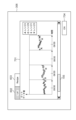
ことを特徴とする情報処理装置。 - 前記表示制御部は、前記第1画面と、前記第1の処理データ及び前記第2の処理データを同じ領域に表示する第2画面とを、前記表示装置に選択的に表示することを特徴とする請求項1に記載の情報処理装置。
- 前記表示制御部は、前記第1画面と共に、前記第1の処理データ及び前記第2の処理データを同じ領域に表示する第2画面を、前記表示装置に表示することを特徴とする請求項1に記載の情報処理装置。
- 基板処理装置による基板処理の処理条件である第1のレシピと、前記第1のレシピが適用された基板処理に関する第1の処理データと、基板処理装置による基板処理の処理条件であり、前記第1のレシピとは異なる第2のレシピと、前記第2のレシピが適用された基板処理に関する第2の処理データとを含む処理情報を取得する取得部と、
前記取得部で取得した前記処理情報に基づいて、表示装置への表示を制御する表示制御部を有し、
前記表示制御部は、前記第1の処理データと、前記第2の処理データとを、それぞれ別の領域に表示する第1画面と、前記第1の処理データ及び前記第2の処理データを同じ領域に表示する第2画面とを、前記表示装置に選択的に表示することを特徴とする情報処理装置。 - 基板処理装置による基板処理の処理条件である第1のレシピと、前記第1のレシピが適用された基板処理に関する第1の処理データと、基板処理装置による基板処理の処理条件であり、前記第1のレシピとは異なる第2のレシピと、前記第2のレシピが適用された基板処理に関する第2の処理データとを含む処理情報を取得する取得部と、
前記取得部で取得した前記処理情報に基づいて、表示装置への表示を制御する表示制御部を有し、
前記表示制御部は、前記第1の処理データと、前記第2の処理データとを、それぞれ別の領域に表示する第1画面と共に、前記第1の処理データ及び前記第2の処理データを同じ領域に表示する第2画面を、前記表示装置に表示することを特徴とする情報処理装置。 - 前記表示制御部は、ユーザによって指定されたロットの処理条件を前記第1画面上に表示することを特徴とする請求項4又は5に記載の情報処理装置。
- 前記表示制御部は、前記第1の処理データ及び前記第2の処理データを同じ時系列で表示する第2画面を、前記表示装置に表示することを特徴とする請求項1乃至6のいずれか1項に記載の情報処理装置。
- 前記第1の処理データ及び前記第2の処理データは、基板処理を行う処理装置の動作結果、及び基板処理が行われた基板を計測することにより得られる、前記基板の状態、を含む情報であることを特徴とする請求項1乃至7のいずれか1項に記載の情報処理装置。
- 前記表示制御部は、処理条件を変更した変更履歴情報を前記第1画面上に表示することを特徴とする請求項1乃至8のいずれか1項に記載の情報処理装置。
- 前記取得部で取得した基板単位の処理データに基づいて、ロット単位の処理データを算出する算出部を更に有することを特徴とする請求項1乃至9のいずれか1項に記載の情報処理装置。
- 前記算出部は、前記取得部で取得した基板単位の処理データの最大値、最小値、平均値、中央値、標準偏差のいずれか1つの統計処理に基づいて、ロット単位の処理データを算出することを特徴とする請求項10に記載の情報処理装置。
- 基板処理装置による基板処理の処理条件である第1のレシピと、前記第1のレシピが適用された基板処理に関する第1の処理データと、基板処理装置による基板処理の処理条件であり、前記第1のレシピとは異なる第2のレシピと、前記第2のレシピが適用された基板処理に関する第2の処理データとを含む処理情報を取得する取得工程と、
前記取得工程で取得した前記処理情報に基づいて、表示装置への表示を制御する表示制御工程を有し、
前記表示制御工程は、
前記第1の処理データと、前記第2の処理データとを、それぞれ別の領域に、且つそれぞれを時系列で、表示する第1画面を、前記表示装置に表示し、
ユーザによって指定されたロットの処理条件を前記第1画面上に表示する、
ことを特徴とする情報処理方法。 - 基板処理装置による基板処理の処理条件である第1のレシピと、前記第1のレシピが適用された基板処理に関する第1の処理データと、基板処理装置による基板処理の処理条件であり、前記第1のレシピとは異なる第2のレシピと、前記第2のレシピが適用された基板処理に関する第2の処理データとを含む処理情報を取得する取得工程と、
前記取得工程で取得した前記処理情報に基づいて、表示装置への表示を制御する表示制御工程を有し、
前記表示制御工程は、前記第1の処理データと、前記第2の処理データとを、それぞれ別の領域に表示する第1画面と、前記第1の処理データ及び前記第2の処理データを同じ領域に表示する第2画面とを、前記表示装置に選択的に表示することを特徴とする情報処理方法。 - 基板処理装置による基板処理の処理条件である第1のレシピと、前記第1のレシピが適用された基板処理に関する第1の処理データと、基板処理装置による基板処理の処理条件であり、前記第1のレシピとは異なる第2のレシピと、前記第2のレシピが適用された基板処理に関する第2の処理データとを含む処理情報を取得する取得工程と、
前記取得工程で取得した前記処理情報に基づいて、表示装置への表示を制御する表示制御工程を有し、
前記表示制御工程は、前記第1の処理データと、前記第2の処理データとを、それぞれ別の領域に表示する第1画面と共に、前記第1の処理データ及び前記第2の処理データを同じ領域に表示する第2画面を、前記表示装置に表示することを特徴とする情報処理方法。 - 請求項12乃至14のいずれか1項に記載の情報処理方法の各工程をコンピュータに実行させるためのプログラム。
- 請求項1乃至11のいずれか1項に記載の情報処理装置と、
基板上にパターンを形成するパターン形成装置と、を含み、
前記情報処理装置は、前記パターン形成装置を含む複数の装置を管理することを特徴とする物品の製造システム。 - 請求項16に記載の製造システムを用いて基板上にパターンを形成する形成工程と、
前記形成工程で前記パターンが形成された前記基板を加工する加工工程と、を含み、
前記加工工程で加工された前記基板から物品を製造することを特徴とする物品の製造方法。
Priority Applications (9)
| Application Number | Priority Date | Filing Date | Title |
|---|---|---|---|
| JP2020079055A JP7570822B2 (ja) | 2020-04-28 | 2020-04-28 | 情報処理装置、及び情報処理方法 |
| SG10202103767WA SG10202103767WA (en) | 2020-04-28 | 2021-04-13 | Information processing apparatus and information processing method |
| TW110113541A TWI820413B (zh) | 2020-04-28 | 2021-04-15 | 資訊處理設備、資訊處理方法、物品製造系統及物品製造方法 |
| KR1020210052051A KR20210133151A (ko) | 2020-04-28 | 2021-04-22 | 정보처리장치 및 정보처리방법 |
| US17/239,332 US11829676B2 (en) | 2020-04-28 | 2021-04-23 | Information processing apparatus and information processing method |
| EP21170546.2A EP3904978A3 (en) | 2020-04-28 | 2021-04-26 | Information processing apparatus and information processing method |
| CN202110465952.0A CN113571444B (zh) | 2020-04-28 | 2021-04-28 | 信息处理装置和信息处理方法 |
| US18/492,587 US12242765B2 (en) | 2020-04-28 | 2023-10-23 | Information processing apparatus and information processing method |
| JP2024172065A JP7732057B2 (ja) | 2020-04-28 | 2024-10-01 | 情報処理装置、及び情報処理方法 |
Applications Claiming Priority (1)
| Application Number | Priority Date | Filing Date | Title |
|---|---|---|---|
| JP2020079055A JP7570822B2 (ja) | 2020-04-28 | 2020-04-28 | 情報処理装置、及び情報処理方法 |
Related Child Applications (1)
| Application Number | Title | Priority Date | Filing Date |
|---|---|---|---|
| JP2024172065A Division JP7732057B2 (ja) | 2020-04-28 | 2024-10-01 | 情報処理装置、及び情報処理方法 |
Publications (3)
| Publication Number | Publication Date |
|---|---|
| JP2021173914A JP2021173914A (ja) | 2021-11-01 |
| JP2021173914A5 JP2021173914A5 (ja) | 2023-05-15 |
| JP7570822B2 true JP7570822B2 (ja) | 2024-10-22 |
Family
ID=75690135
Family Applications (2)
| Application Number | Title | Priority Date | Filing Date |
|---|---|---|---|
| JP2020079055A Active JP7570822B2 (ja) | 2020-04-28 | 2020-04-28 | 情報処理装置、及び情報処理方法 |
| JP2024172065A Active JP7732057B2 (ja) | 2020-04-28 | 2024-10-01 | 情報処理装置、及び情報処理方法 |
Family Applications After (1)
| Application Number | Title | Priority Date | Filing Date |
|---|---|---|---|
| JP2024172065A Active JP7732057B2 (ja) | 2020-04-28 | 2024-10-01 | 情報処理装置、及び情報処理方法 |
Country Status (7)
| Country | Link |
|---|---|
| US (2) | US11829676B2 (ja) |
| EP (1) | EP3904978A3 (ja) |
| JP (2) | JP7570822B2 (ja) |
| KR (1) | KR20210133151A (ja) |
| CN (1) | CN113571444B (ja) |
| SG (1) | SG10202103767WA (ja) |
| TW (1) | TWI820413B (ja) |
Families Citing this family (2)
| Publication number | Priority date | Publication date | Assignee | Title |
|---|---|---|---|---|
| JP7665347B2 (ja) * | 2021-02-04 | 2025-04-21 | キヤノン株式会社 | 情報処理装置、及び情報処理方法 |
| CN116262440A (zh) * | 2021-12-14 | 2023-06-16 | 荷兰移动驱动器公司 | 系统界面控制方法、车辆终端及计算机可读存储介质 |
Citations (6)
| Publication number | Priority date | Publication date | Assignee | Title |
|---|---|---|---|---|
| JP2005093922A (ja) | 2003-09-19 | 2005-04-07 | Dainippon Screen Mfg Co Ltd | 基板処理システム |
| WO2005045907A1 (ja) | 2003-11-10 | 2005-05-19 | Renesas Technology Corp. | 半導体集積回路装置の製造方法 |
| WO2006019166A1 (ja) | 2004-08-19 | 2006-02-23 | Nikon Corporation | アライメント情報表示方法とそのプログラム、アライメント方法、露光方法、デバイス製造方法、表示システム、表示装置、プログラム及び測定/検査装置 |
| JP2007042701A (ja) | 2005-08-01 | 2007-02-15 | Nikon Corp | 情報表示システム |
| US20130253866A1 (en) | 2010-11-13 | 2013-09-26 | Abb Technology Ag | Intelligent visualisation in the monitoring of process and/or system variables |
| JP2014529909A (ja) | 2011-09-01 | 2014-11-13 | ケーエルエー−テンカー コーポレイション | 問題のある高度プロセス制御パラメータの検出及び訂正のための方法及びシステム |
Family Cites Families (31)
| Publication number | Priority date | Publication date | Assignee | Title |
|---|---|---|---|---|
| JP3413074B2 (ja) * | 1997-08-29 | 2003-06-03 | キヤノン株式会社 | 露光装置およびデバイス製造方法 |
| US8028249B2 (en) * | 2001-05-23 | 2011-09-27 | Eastman Kodak Company | Method and system for browsing large digital multimedia object collections |
| JP2003168297A (ja) * | 2001-11-28 | 2003-06-13 | Nec Electronics Corp | 半導体検査装置、半導体不良情報の表示処理方法及び表示処理プログラムを記録した記録媒体 |
| WO2006016435A1 (ja) * | 2004-08-11 | 2006-02-16 | Tokyo Electron Limited | 処理システムおよび処理方法、ならびにコンピュータ読取可能な記憶媒体およびコンピュータプログラム |
| JP4413767B2 (ja) * | 2004-12-17 | 2010-02-10 | 株式会社日立ハイテクノロジーズ | パターン検査装置 |
| JP2006237052A (ja) | 2005-02-22 | 2006-09-07 | Nikon System:Kk | 情報表示方法、情報表示プログラム、情報表示装置及びデバイス製造システム、並びに基板処理装置 |
| JP2007033785A (ja) * | 2005-07-26 | 2007-02-08 | Sony Corp | 情報処理装置および方法、並びにプログラム |
| JP5224656B2 (ja) * | 2006-05-31 | 2013-07-03 | 東京エレクトロン株式会社 | 情報処理装置、半導体製造システム、情報処理方法、プログラム、及び記録媒体 |
| JP5291911B2 (ja) * | 2007-09-28 | 2013-09-18 | 株式会社日立ハイテクノロジーズ | 計測システム |
| JP2009170612A (ja) | 2008-01-15 | 2009-07-30 | Canon Inc | 情報処理装置、情報処理方法、処理システムおよびコンピュータプログラム |
| KR20100035474A (ko) * | 2008-09-26 | 2010-04-05 | 삼성전자주식회사 | 휴대 단말기의 컨텐츠 리스트 표시 방법 |
| JP2010210527A (ja) * | 2009-03-11 | 2010-09-24 | Horiba Ltd | 異物検査除去装置及び異物検査除去プログラム |
| JP2011044458A (ja) * | 2009-08-19 | 2011-03-03 | Hitachi Kokusai Electric Inc | 基板処理システム |
| JP5133322B2 (ja) * | 2009-10-22 | 2013-01-30 | 株式会社アルバック | 真空処理装置、グラフ線表示方法 |
| JP2011129580A (ja) * | 2009-12-15 | 2011-06-30 | Toshiba Corp | 異常装置検出システムおよび異常装置検出プログラム |
| US8655469B2 (en) * | 2010-06-14 | 2014-02-18 | Kla-Tencor Corporation | Advanced process control optimization |
| JP5600503B2 (ja) * | 2010-07-06 | 2014-10-01 | 株式会社日立国際電気 | 統計解析方法、基板処理システムおよびプログラム |
| CA2790799C (en) * | 2011-09-25 | 2023-03-21 | Mathieu Audet | Method and apparatus of navigating information element axes |
| JP5742635B2 (ja) * | 2011-09-29 | 2015-07-01 | 東京エレクトロン株式会社 | 基板処理装置、基板処理装置のアラーム管理方法および記憶媒体 |
| US9830050B2 (en) * | 2011-11-23 | 2017-11-28 | Salesforce.Com, Inc. | Computer implemented methods and apparatus for providing a reminder regarding a feed item of a feed of an online social network |
| WO2013125387A1 (ja) | 2012-02-23 | 2013-08-29 | 株式会社日立国際電気 | 基板処理システム、管理装置、及び表示方法 |
| CN103293878B (zh) | 2013-05-31 | 2015-07-15 | 上海华力微电子有限公司 | 光刻机产能监测系统 |
| US10572103B2 (en) * | 2014-09-30 | 2020-02-25 | Apple Inc. | Timeline view of recently opened documents |
| GB2547388A (en) * | 2014-11-21 | 2017-08-16 | Big Sky Sorcery Llc | System and method for searching structured data files |
| JP6340347B2 (ja) * | 2015-07-24 | 2018-06-06 | 富士フイルム株式会社 | 画像処理装置、画像処理方法、プログラムおよび記録媒体 |
| JP6581718B2 (ja) | 2016-03-14 | 2019-09-25 | 株式会社Kokusai Electric | 基板処理装置、コントローラ及び部品管理プログラム |
| JP6877200B2 (ja) | 2017-03-15 | 2021-05-26 | 東京エレクトロン株式会社 | 基板処理装置の制御装置及び基板処理表示方法 |
| JP6808684B2 (ja) | 2018-06-14 | 2021-01-06 | キヤノン株式会社 | 情報処理装置、判定方法、プログラム、リソグラフィシステム、および物品の製造方法 |
| EP3671707A1 (en) * | 2018-12-21 | 2020-06-24 | IMEC vzw | Improved coding for avoiding motion artefacts |
| JP2020146286A (ja) * | 2019-03-14 | 2020-09-17 | 株式会社リコー | 情報処理装置、情報処理方法、プログラムおよび生体信号計測システム |
| US20210035301A1 (en) * | 2019-07-31 | 2021-02-04 | Nikon Corporation | Information processing system, information processing apparatus, recording medium, and information processing method |
-
2020
- 2020-04-28 JP JP2020079055A patent/JP7570822B2/ja active Active
-
2021
- 2021-04-13 SG SG10202103767WA patent/SG10202103767WA/en unknown
- 2021-04-15 TW TW110113541A patent/TWI820413B/zh active
- 2021-04-22 KR KR1020210052051A patent/KR20210133151A/ko active Pending
- 2021-04-23 US US17/239,332 patent/US11829676B2/en active Active
- 2021-04-26 EP EP21170546.2A patent/EP3904978A3/en active Pending
- 2021-04-28 CN CN202110465952.0A patent/CN113571444B/zh active Active
-
2023
- 2023-10-23 US US18/492,587 patent/US12242765B2/en active Active
-
2024
- 2024-10-01 JP JP2024172065A patent/JP7732057B2/ja active Active
Patent Citations (6)
| Publication number | Priority date | Publication date | Assignee | Title |
|---|---|---|---|---|
| JP2005093922A (ja) | 2003-09-19 | 2005-04-07 | Dainippon Screen Mfg Co Ltd | 基板処理システム |
| WO2005045907A1 (ja) | 2003-11-10 | 2005-05-19 | Renesas Technology Corp. | 半導体集積回路装置の製造方法 |
| WO2006019166A1 (ja) | 2004-08-19 | 2006-02-23 | Nikon Corporation | アライメント情報表示方法とそのプログラム、アライメント方法、露光方法、デバイス製造方法、表示システム、表示装置、プログラム及び測定/検査装置 |
| JP2007042701A (ja) | 2005-08-01 | 2007-02-15 | Nikon Corp | 情報表示システム |
| US20130253866A1 (en) | 2010-11-13 | 2013-09-26 | Abb Technology Ag | Intelligent visualisation in the monitoring of process and/or system variables |
| JP2014529909A (ja) | 2011-09-01 | 2014-11-13 | ケーエルエー−テンカー コーポレイション | 問題のある高度プロセス制御パラメータの検出及び訂正のための方法及びシステム |
Also Published As
| Publication number | Publication date |
|---|---|
| US12242765B2 (en) | 2025-03-04 |
| US11829676B2 (en) | 2023-11-28 |
| SG10202103767WA (en) | 2021-11-29 |
| CN113571444A (zh) | 2021-10-29 |
| US20240053941A1 (en) | 2024-02-15 |
| KR20210133151A (ko) | 2021-11-05 |
| CN113571444B (zh) | 2026-03-17 |
| TW202209000A (zh) | 2022-03-01 |
| JP2024178459A (ja) | 2024-12-24 |
| US20210333721A1 (en) | 2021-10-28 |
| EP3904978A3 (en) | 2022-01-12 |
| TWI820413B (zh) | 2023-11-01 |
| JP7732057B2 (ja) | 2025-09-01 |
| EP3904978A2 (en) | 2021-11-03 |
| JP2021173914A (ja) | 2021-11-01 |
Similar Documents
| Publication | Publication Date | Title |
|---|---|---|
| EP3582011B1 (en) | Information processing apparatus, method, program, lithography system, and manufacturing method of article | |
| JP7732057B2 (ja) | 情報処理装置、及び情報処理方法 | |
| US6456374B1 (en) | Exposure apparatus and a device manufacturing method using the same | |
| JP7732048B2 (ja) | 情報処理装置、及び情報処理方法 | |
| JP7665347B2 (ja) | 情報処理装置、及び情報処理方法 | |
| US12362209B2 (en) | Information processing apparatus, information processing method, article manufacturing system, and article manufacturing method | |
| JP2026049857A (ja) | 設定方法、制御方法、及び情報処理装置 |
Legal Events
| Date | Code | Title | Description |
|---|---|---|---|
| RD01 | Notification of change of attorney |
Free format text: JAPANESE INTERMEDIATE CODE: A7421 Effective date: 20200616 |
|
| A521 | Request for written amendment filed |
Free format text: JAPANESE INTERMEDIATE CODE: A523 Effective date: 20230421 |
|
| A621 | Written request for application examination |
Free format text: JAPANESE INTERMEDIATE CODE: A621 Effective date: 20230421 |
|
| A521 | Request for written amendment filed |
Free format text: JAPANESE INTERMEDIATE CODE: A523 Effective date: 20230502 |
|
| RD01 | Notification of change of attorney |
Free format text: JAPANESE INTERMEDIATE CODE: A7421 Effective date: 20231213 |
|
| A977 | Report on retrieval |
Free format text: JAPANESE INTERMEDIATE CODE: A971007 Effective date: 20240105 |
|
| A131 | Notification of reasons for refusal |
Free format text: JAPANESE INTERMEDIATE CODE: A131 Effective date: 20240116 |
|
| A521 | Request for written amendment filed |
Free format text: JAPANESE INTERMEDIATE CODE: A523 Effective date: 20240306 |
|
| A131 | Notification of reasons for refusal |
Free format text: JAPANESE INTERMEDIATE CODE: A131 Effective date: 20240430 |
|
| A521 | Request for written amendment filed |
Free format text: JAPANESE INTERMEDIATE CODE: A523 Effective date: 20240612 |
|
| TRDD | Decision of grant or rejection written | ||
| A01 | Written decision to grant a patent or to grant a registration (utility model) |
Free format text: JAPANESE INTERMEDIATE CODE: A01 Effective date: 20240910 |
|
| A61 | First payment of annual fees (during grant procedure) |
Free format text: JAPANESE INTERMEDIATE CODE: A61 Effective date: 20241009 |
|
| R150 | Certificate of patent or registration of utility model |
Ref document number: 7570822 Country of ref document: JP Free format text: JAPANESE INTERMEDIATE CODE: R150 |