JP7546397B2 - インダクタ - Google Patents
インダクタ Download PDFInfo
- Publication number
- JP7546397B2 JP7546397B2 JP2020126344A JP2020126344A JP7546397B2 JP 7546397 B2 JP7546397 B2 JP 7546397B2 JP 2020126344 A JP2020126344 A JP 2020126344A JP 2020126344 A JP2020126344 A JP 2020126344A JP 7546397 B2 JP7546397 B2 JP 7546397B2
- Authority
- JP
- Japan
- Prior art keywords
- wiring
- thickness direction
- inductor
- main surface
- layer
- Prior art date
- Legal status (The legal status is an assumption and is not a legal conclusion. Google has not performed a legal analysis and makes no representation as to the accuracy of the status listed.)
- Active
Links
Images


Classifications
-
- H—ELECTRICITY
- H01—ELECTRIC ELEMENTS
- H01F—MAGNETS; INDUCTANCES; TRANSFORMERS; SELECTION OF MATERIALS FOR THEIR MAGNETIC PROPERTIES
- H01F17/00—Fixed inductances of the signal type
- H01F17/04—Fixed inductances of the signal type with magnetic core
-
- H—ELECTRICITY
- H01—ELECTRIC ELEMENTS
- H01F—MAGNETS; INDUCTANCES; TRANSFORMERS; SELECTION OF MATERIALS FOR THEIR MAGNETIC PROPERTIES
- H01F27/00—Details of transformers or inductances, in general
- H01F27/28—Coils; Windings; Conductive connections
- H01F27/2823—Wires
- H01F27/2828—Construction of conductive connections, of leads
-
- H—ELECTRICITY
- H01—ELECTRIC ELEMENTS
- H01F—MAGNETS; INDUCTANCES; TRANSFORMERS; SELECTION OF MATERIALS FOR THEIR MAGNETIC PROPERTIES
- H01F17/00—Fixed inductances of the signal type
- H01F17/0006—Printed inductances
- H01F17/0013—Printed inductances with stacked layers
-
- H—ELECTRICITY
- H01—ELECTRIC ELEMENTS
- H01F—MAGNETS; INDUCTANCES; TRANSFORMERS; SELECTION OF MATERIALS FOR THEIR MAGNETIC PROPERTIES
- H01F1/00—Magnets or magnetic bodies characterised by the magnetic materials therefor; Selection of materials for their magnetic properties
- H01F1/01—Magnets or magnetic bodies characterised by the magnetic materials therefor; Selection of materials for their magnetic properties of inorganic materials
- H01F1/03—Magnets or magnetic bodies characterised by the magnetic materials therefor; Selection of materials for their magnetic properties of inorganic materials characterised by their coercivity
- H01F1/12—Magnets or magnetic bodies characterised by the magnetic materials therefor; Selection of materials for their magnetic properties of inorganic materials characterised by their coercivity of soft-magnetic materials
- H01F1/14—Magnets or magnetic bodies characterised by the magnetic materials therefor; Selection of materials for their magnetic properties of inorganic materials characterised by their coercivity of soft-magnetic materials metals or alloys
- H01F1/20—Magnets or magnetic bodies characterised by the magnetic materials therefor; Selection of materials for their magnetic properties of inorganic materials characterised by their coercivity of soft-magnetic materials metals or alloys in the form of particles, e.g. powder
-
- H—ELECTRICITY
- H01—ELECTRIC ELEMENTS
- H01F—MAGNETS; INDUCTANCES; TRANSFORMERS; SELECTION OF MATERIALS FOR THEIR MAGNETIC PROPERTIES
- H01F17/00—Fixed inductances of the signal type
- H01F17/04—Fixed inductances of the signal type with magnetic core
- H01F17/06—Fixed inductances of the signal type with magnetic core with core substantially closed in itself, e.g. toroid
-
- H—ELECTRICITY
- H01—ELECTRIC ELEMENTS
- H01F—MAGNETS; INDUCTANCES; TRANSFORMERS; SELECTION OF MATERIALS FOR THEIR MAGNETIC PROPERTIES
- H01F27/00—Details of transformers or inductances, in general
- H01F27/24—Magnetic cores
-
- H—ELECTRICITY
- H01—ELECTRIC ELEMENTS
- H01F—MAGNETS; INDUCTANCES; TRANSFORMERS; SELECTION OF MATERIALS FOR THEIR MAGNETIC PROPERTIES
- H01F27/00—Details of transformers or inductances, in general
- H01F27/24—Magnetic cores
- H01F27/255—Magnetic cores made from particles
-
- H—ELECTRICITY
- H01—ELECTRIC ELEMENTS
- H01F—MAGNETS; INDUCTANCES; TRANSFORMERS; SELECTION OF MATERIALS FOR THEIR MAGNETIC PROPERTIES
- H01F27/00—Details of transformers or inductances, in general
- H01F27/28—Coils; Windings; Conductive connections
- H01F27/2823—Wires
-
- H—ELECTRICITY
- H01—ELECTRIC ELEMENTS
- H01F—MAGNETS; INDUCTANCES; TRANSFORMERS; SELECTION OF MATERIALS FOR THEIR MAGNETIC PROPERTIES
- H01F27/00—Details of transformers or inductances, in general
- H01F27/28—Coils; Windings; Conductive connections
- H01F27/32—Insulating of coils, windings, or parts thereof
- H01F27/324—Insulation between coil and core, between different winding sections, around the coil; Other insulation structures
-
- H—ELECTRICITY
- H01—ELECTRIC ELEMENTS
- H01F—MAGNETS; INDUCTANCES; TRANSFORMERS; SELECTION OF MATERIALS FOR THEIR MAGNETIC PROPERTIES
- H01F41/00—Apparatus or processes specially adapted for manufacturing or assembling magnets, inductances or transformers; Apparatus or processes specially adapted for manufacturing materials characterised by their magnetic properties
- H01F41/02—Apparatus or processes specially adapted for manufacturing or assembling magnets, inductances or transformers; Apparatus or processes specially adapted for manufacturing materials characterised by their magnetic properties for manufacturing cores, coils, or magnets
- H01F41/0206—Manufacturing of magnetic cores by mechanical means
-
- H—ELECTRICITY
- H01—ELECTRIC ELEMENTS
- H01F—MAGNETS; INDUCTANCES; TRANSFORMERS; SELECTION OF MATERIALS FOR THEIR MAGNETIC PROPERTIES
- H01F41/00—Apparatus or processes specially adapted for manufacturing or assembling magnets, inductances or transformers; Apparatus or processes specially adapted for manufacturing materials characterised by their magnetic properties
- H01F41/02—Apparatus or processes specially adapted for manufacturing or assembling magnets, inductances or transformers; Apparatus or processes specially adapted for manufacturing materials characterised by their magnetic properties for manufacturing cores, coils, or magnets
- H01F41/04—Apparatus or processes specially adapted for manufacturing or assembling magnets, inductances or transformers; Apparatus or processes specially adapted for manufacturing materials characterised by their magnetic properties for manufacturing cores, coils, or magnets for manufacturing coils
- H01F41/06—Coil winding
- H01F41/064—Winding non-flat conductive wires, e.g. rods, cables or cords
- H01F41/066—Winding non-flat conductive wires, e.g. rods, cables or cords with insulation
-
- H—ELECTRICITY
- H01—ELECTRIC ELEMENTS
- H01F—MAGNETS; INDUCTANCES; TRANSFORMERS; SELECTION OF MATERIALS FOR THEIR MAGNETIC PROPERTIES
- H01F17/00—Fixed inductances of the signal type
- H01F17/0006—Printed inductances
- H01F17/0013—Printed inductances with stacked layers
- H01F2017/002—Details of via holes for interconnecting the layers
-
- H—ELECTRICITY
- H01—ELECTRIC ELEMENTS
- H01F—MAGNETS; INDUCTANCES; TRANSFORMERS; SELECTION OF MATERIALS FOR THEIR MAGNETIC PROPERTIES
- H01F17/00—Fixed inductances of the signal type
- H01F17/04—Fixed inductances of the signal type with magnetic core
- H01F2017/048—Fixed inductances of the signal type with magnetic core with encapsulating core, e.g. made of resin and magnetic powder
-
- H—ELECTRICITY
- H01—ELECTRIC ELEMENTS
- H01F—MAGNETS; INDUCTANCES; TRANSFORMERS; SELECTION OF MATERIALS FOR THEIR MAGNETIC PROPERTIES
- H01F17/00—Fixed inductances of the signal type
- H01F17/04—Fixed inductances of the signal type with magnetic core
- H01F17/06—Fixed inductances of the signal type with magnetic core with core substantially closed in itself, e.g. toroid
- H01F2017/065—Core mounted around conductor to absorb noise, e.g. EMI filter
Landscapes
- Engineering & Computer Science (AREA)
- Power Engineering (AREA)
- Microelectronics & Electronic Packaging (AREA)
- Manufacturing & Machinery (AREA)
- Chemical & Material Sciences (AREA)
- Dispersion Chemistry (AREA)
- Coils Or Transformers For Communication (AREA)
Description
[第1実施形態に対応する実施例]
砥粒子の材料:アルミナ
砥粒子のメジアン径:14μm
噴射速度:0.4MPa
[第2実施形態に対応する実施例]
図13に示すように、実施例1のインダクタ1に、加工安定層24と第2加工安定層25とを備えた。
[第3実施形態に対応する実施例]
図14に示すように、実施例2の加工安定層24にビア10を形成した。
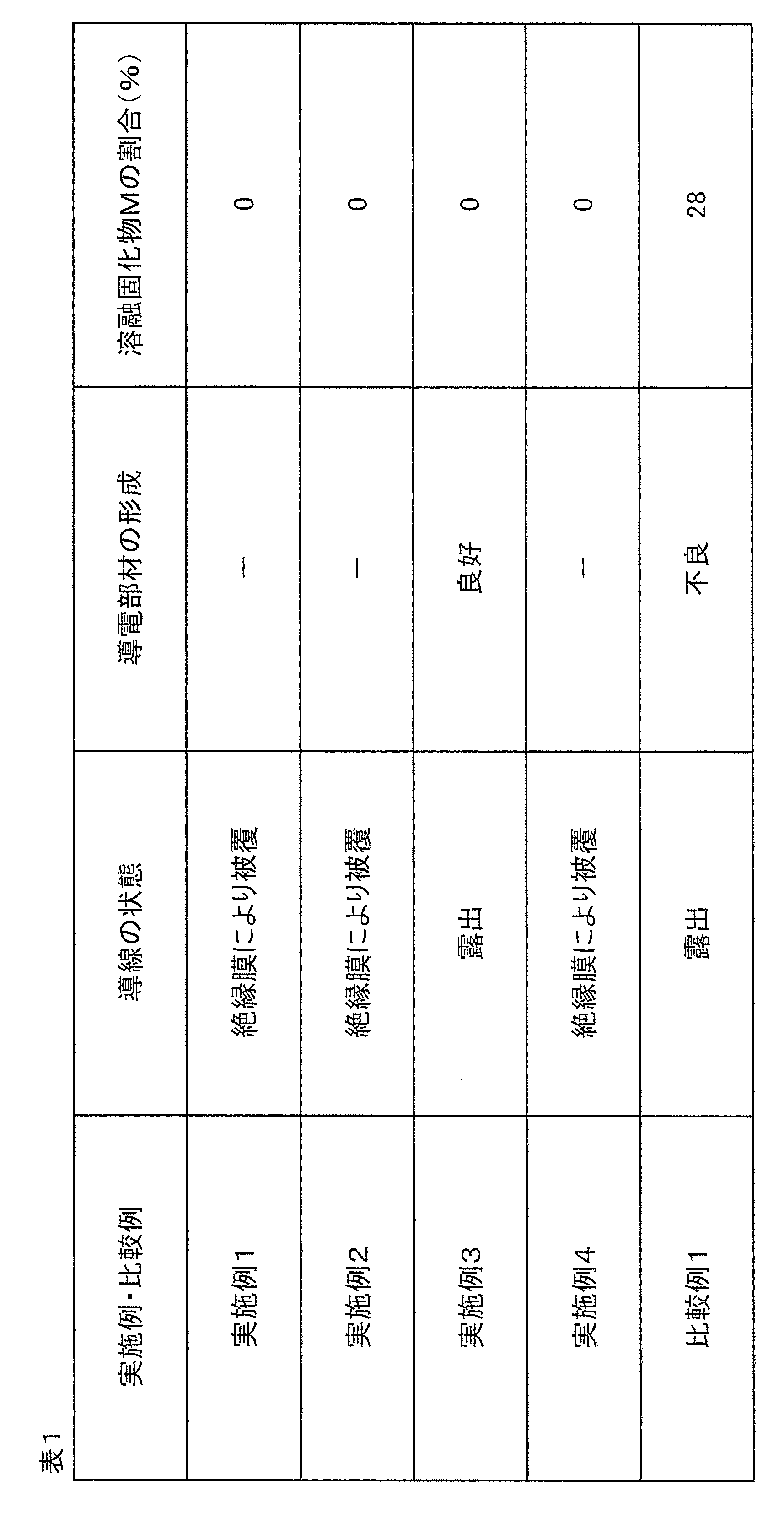
開口部22の直径を100μmに変更した以外は、実施例1と同様に処理した。図11Aに示すように、内周面9は、テーパ面27と、第2テーパ面28とを有していた。
ブラスト法に代え、レーザー加工に変更した以外は、実施例1と同様に処理した。導線4は、レーザー加工によって、露出した。さらに、導電部材19を電解銅めっきにより形成しようと試みた。しかし、導電部材19の形成に不良が生じた。
SEM観察、溶融固化物Mの割合および導電部材の形成
[不良] 導電部材19が溶融固化物Mを介して形成されていた。
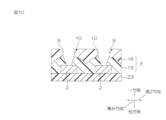
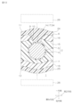
2 配線
3 磁性層
4 導線
4 配線
5 絶縁膜
6 第1主面
7 第2主面
9 内周面
10 ビア
11 一方面
13 段差
24 加工安定層
27 テーパ面
28 第2テーパ面
34 方向一方面
34 一方面
35 突出端部
M 溶融固化物
P1 第1点
P2 第2点
P3 第3点
P4 第4点
E1 第1端縁
E2 第2端縁
Claims (10)
- 配線と、
前記配線を埋設し、磁性粒子を含有する磁性層とを備えるインダクタであって、
前記磁性層は、
前記配線に対して厚み方向一方側に間隔を隔てて配置される第1主面と、
前記第1主面と厚み方向に間隔を隔てられ、前記配線に対して前記第1主面の反対側に配置される第2主面と、
前記第1主面から前記配線に向かって貫通するビアとを有し、
前記ビアは、厚み方向から見たときに無端形状である内周面を有し、
1つの前記ビアにおいて、前記内周面は、段差を有し、
下記の方法によって求められる溶融固化物の百分率が、10%以下であることを特徴とする、インダクタ。
前記ビアを横断する断面において、前記内周面の厚み方向一方側の端縁を基準として前記第1主面が延びる方向の一方側と他方側とにそれぞれ50μm離れて位置する第1点と第2点と、前記内周面の厚み方向他方側の端縁を基準として前記延びる方向の一方側と他方側とにそれぞれ50μm離れて位置する第3点と第4点とを頂点とする四角形の面積S0を取得する。前記四角形の内部に位置する前記溶融固化物の面積S1を取得する。前記四角形の前記面積S0に対する前記溶融固化物の前記面積S1の百分率(S1/S0×100)を求める。 - 1つ前記ビアにおいて、前記内周面にある段差の数が、1であることを特徴とする、請求項1に記載のインダクタ。
- 前記内周面は、前記第1主面に近づくにつれて、前記ビアの開口断面積が大きくなるテーパ面を有することを特徴とする、請求項1または2に記載のインダクタ。
- 前記配線が延びる方向の断面で、前記ビアから露出する前記配線の厚み方向一方面は、平坦形状であることを特徴とする、請求項1~3のいずれか一項に記載のインダクタ。
- 前記配線は、導線と、前記導線の周面に配置される絶縁膜とを備え、
前記絶縁膜は、前記ビアから露出していることを特徴とする、請求項1~4のいずれか一項に記載のインダクタ。 - 前記ビアに充填される加工安定層をさらに備えることを特徴とする、請求項1~5のいずれか一項に記載のインダクタ。
- 前記配線は、導線と、前記導線の周面に配置される絶縁膜とを備え、
前記絶縁膜は、前記ビアにおいて、前記内周面の他端縁から内側に突出する突出端部を有し、
前記突出端部の厚み方向一方面と前記内周面とに配置される加工安定層をさらに備え、
前記突出端部と前記加工安定層とは、前記導線の厚み方向一方面を露出していることを特徴とする、請求項1~4のいずれか一項に記載のインダクタ。 - 前記加工安定層は、さらに、第1主面に配置されていることを特徴とする、請求項6または7に記載のインダクタ。
- 前記磁性粒子が、軟磁性粒子であることを特徴とする、請求項1~8のいずれか一項に記載のインダクタ。
- 前記ビアは、厚み方向に直交する面方向における最長長さD1と最短長さD2とを有し、
前記最短長さD2に対する前記最長長さD1の比(D1/D2)が、10以下であることを特徴とする、請求項1~9のいずれか一項に記載のインダクタ。
Priority Applications (5)
| Application Number | Priority Date | Filing Date | Title |
|---|---|---|---|
| JP2020126344A JP7546397B2 (ja) | 2020-07-27 | 2020-07-27 | インダクタ |
| KR1020210093884A KR20220013912A (ko) | 2020-07-27 | 2021-07-19 | 인덕터 |
| US17/381,745 US12444532B2 (en) | 2020-07-27 | 2021-07-21 | Inductor |
| CN202110836587.XA CN113990603B (zh) | 2020-07-27 | 2021-07-23 | 电感器 |
| TW110127338A TW202205318A (zh) | 2020-07-27 | 2021-07-26 | 電感器 |
Applications Claiming Priority (1)
| Application Number | Priority Date | Filing Date | Title |
|---|---|---|---|
| JP2020126344A JP7546397B2 (ja) | 2020-07-27 | 2020-07-27 | インダクタ |
Publications (2)
| Publication Number | Publication Date |
|---|---|
| JP2022023413A JP2022023413A (ja) | 2022-02-08 |
| JP7546397B2 true JP7546397B2 (ja) | 2024-09-06 |
Family
ID=79688626
Family Applications (1)
| Application Number | Title | Priority Date | Filing Date |
|---|---|---|---|
| JP2020126344A Active JP7546397B2 (ja) | 2020-07-27 | 2020-07-27 | インダクタ |
Country Status (5)
| Country | Link |
|---|---|
| US (1) | US12444532B2 (ja) |
| JP (1) | JP7546397B2 (ja) |
| KR (1) | KR20220013912A (ja) |
| CN (1) | CN113990603B (ja) |
| TW (1) | TW202205318A (ja) |
Citations (7)
| Publication number | Priority date | Publication date | Assignee | Title |
|---|---|---|---|---|
| US20100265030A1 (en) | 2009-04-17 | 2010-10-21 | Nxp B.V. | Inductive components for dc/dc converters and methods of manufacture thereof |
| JP2015088753A (ja) | 2013-10-29 | 2015-05-07 | サムソン エレクトロ−メカニックス カンパニーリミテッド. | コイル部品とその製造方法、コイル部品内蔵基板、及びこれを含む電圧調節モジュール |
| JP2017098544A (ja) | 2015-11-20 | 2017-06-01 | サムソン エレクトロ−メカニックス カンパニーリミテッド. | コイル部品 |
| JP2017112130A (ja) | 2015-12-14 | 2017-06-22 | 株式会社村田製作所 | 電子部品及びその製造方法 |
| JP2017216401A (ja) | 2016-06-01 | 2017-12-07 | 株式会社村田製作所 | 電子部品 |
| JP2019160929A (ja) | 2018-03-09 | 2019-09-19 | 日東電工株式会社 | 配線基板およびその製造方法 |
| JP2020088285A (ja) | 2018-11-29 | 2020-06-04 | 味の素株式会社 | 基板の製造方法 |
Family Cites Families (12)
| Publication number | Priority date | Publication date | Assignee | Title |
|---|---|---|---|---|
| JP3197022B2 (ja) * | 1991-05-13 | 2001-08-13 | ティーディーケイ株式会社 | ノイズサプレッサ用積層セラミック部品 |
| US7161089B2 (en) * | 2002-12-04 | 2007-01-09 | Tdk Corporation | Electronic component |
| JP6062691B2 (ja) | 2012-04-25 | 2017-01-18 | Necトーキン株式会社 | シート状インダクタ、積層基板内蔵型インダクタ及びそれらの製造方法 |
| JP2014078546A (ja) | 2012-10-09 | 2014-05-01 | Panasonic Corp | 積層インダクタの製造方法 |
| JP2015199131A (ja) | 2014-04-04 | 2015-11-12 | 株式会社アルプスエンジニアリング | 研磨材噴射装置 |
| JP6413654B2 (ja) | 2014-11-04 | 2018-10-31 | 味の素株式会社 | 回路基板及びその製造方法 |
| KR102450597B1 (ko) * | 2017-09-29 | 2022-10-07 | 삼성전기주식회사 | 코일 부품 및 그의 제조방법 |
| JP7372747B2 (ja) | 2018-03-16 | 2023-11-01 | 日東電工株式会社 | 配線回路基板およびその製造方法 |
| JP7352363B2 (ja) | 2018-03-16 | 2023-09-28 | 日東電工株式会社 | 磁性配線回路基板およびその製造方法 |
| JP7220948B2 (ja) | 2018-04-09 | 2023-02-13 | 日東電工株式会社 | 磁性配線回路基板 |
| JP7223525B2 (ja) * | 2018-08-09 | 2023-02-16 | 新光電気工業株式会社 | インダクタ及びインダクタの製造方法 |
| KR102662847B1 (ko) * | 2019-09-30 | 2024-05-03 | 삼성전기주식회사 | 인쇄회로기판 |
-
2020
- 2020-07-27 JP JP2020126344A patent/JP7546397B2/ja active Active
-
2021
- 2021-07-19 KR KR1020210093884A patent/KR20220013912A/ko active Pending
- 2021-07-21 US US17/381,745 patent/US12444532B2/en active Active
- 2021-07-23 CN CN202110836587.XA patent/CN113990603B/zh active Active
- 2021-07-26 TW TW110127338A patent/TW202205318A/zh unknown
Patent Citations (7)
| Publication number | Priority date | Publication date | Assignee | Title |
|---|---|---|---|---|
| US20100265030A1 (en) | 2009-04-17 | 2010-10-21 | Nxp B.V. | Inductive components for dc/dc converters and methods of manufacture thereof |
| JP2015088753A (ja) | 2013-10-29 | 2015-05-07 | サムソン エレクトロ−メカニックス カンパニーリミテッド. | コイル部品とその製造方法、コイル部品内蔵基板、及びこれを含む電圧調節モジュール |
| JP2017098544A (ja) | 2015-11-20 | 2017-06-01 | サムソン エレクトロ−メカニックス カンパニーリミテッド. | コイル部品 |
| JP2017112130A (ja) | 2015-12-14 | 2017-06-22 | 株式会社村田製作所 | 電子部品及びその製造方法 |
| JP2017216401A (ja) | 2016-06-01 | 2017-12-07 | 株式会社村田製作所 | 電子部品 |
| JP2019160929A (ja) | 2018-03-09 | 2019-09-19 | 日東電工株式会社 | 配線基板およびその製造方法 |
| JP2020088285A (ja) | 2018-11-29 | 2020-06-04 | 味の素株式会社 | 基板の製造方法 |
Also Published As
| Publication number | Publication date |
|---|---|
| TW202205318A (zh) | 2022-02-01 |
| US20220028599A1 (en) | 2022-01-27 |
| CN113990603A (zh) | 2022-01-28 |
| KR20220013912A (ko) | 2022-02-04 |
| US12444532B2 (en) | 2025-10-14 |
| CN113990603B (zh) | 2026-02-13 |
| JP2022023413A (ja) | 2022-02-08 |
Similar Documents
| Publication | Publication Date | Title |
|---|---|---|
| EP1986200B1 (en) | Composite magnetic sheet and process for producing the same | |
| KR100918339B1 (ko) | 프린트 배선판의 내장 캐패시터층 형성용의 유전체필러함유 수지 및 그 유전체 필러함유 수지를 사용하여유전체층을 형성한 양면 동클래드 적층판 및 그 양면동클래드 적층판의 제조방법 | |
| KR100832628B1 (ko) | 도전 페이스트 | |
| JP7565721B2 (ja) | インダクタの製造方法 | |
| US7083859B2 (en) | Conductive powder and method for preparing the same | |
| WO2002035554A1 (en) | Electroconductive metal paste and method for production thereof | |
| KR100685273B1 (ko) | 절연재료, 필름, 회로기판 및 이들의 제조방법 | |
| CN111937501A (zh) | 固化性树脂组合物、其固化物和印刷电路板 | |
| JP4235888B2 (ja) | 導電ペースト | |
| KR20190092404A (ko) | 패키지 기판 및 패키지 기판의 제조 방법 | |
| WO2004027787A1 (ja) | 電子デバイスの電気的接続用導電性組成物および電子デバイス | |
| TW202100342A (zh) | 導電性接著片 | |
| TWI847061B (zh) | 電磁波屏蔽膜及屏蔽印刷配線板 | |
| JP7546397B2 (ja) | インダクタ | |
| JP5344097B2 (ja) | 半導体封止充てん用フィルム状樹脂組成物、半導体装置の製造方法及び半導体装置 | |
| JP5609492B2 (ja) | 電子部品及びその製造方法 | |
| JP2022060975A (ja) | インダクタ、及びインダクタの製造方法 | |
| JP2011228481A (ja) | 導電性ペースト、フレキシブルプリント配線板、電子機器 | |
| JP2022060995A (ja) | 軟磁性粉及びインダクタ | |
| JP7069967B2 (ja) | 放熱基板 | |
| JP6006539B2 (ja) | 回路基板及び電子部品搭載基板 | |
| JP2021086912A (ja) | 電子部品搭載基板および電子機器 | |
| JP2004127537A (ja) | 電極形成用導電性熱硬化性樹脂組成物 | |
| JP2001302884A (ja) | 導電ペースト | |
| WO2023190423A1 (ja) | 導電性接着剤層及び放熱構造 |
Legal Events
| Date | Code | Title | Description |
|---|---|---|---|
| A621 | Written request for application examination |
Free format text: JAPANESE INTERMEDIATE CODE: A621 Effective date: 20230601 |
|
| A131 | Notification of reasons for refusal |
Free format text: JAPANESE INTERMEDIATE CODE: A131 Effective date: 20240109 |
|
| A977 | Report on retrieval |
Free format text: JAPANESE INTERMEDIATE CODE: A971007 Effective date: 20240111 |
|
| A601 | Written request for extension of time |
Free format text: JAPANESE INTERMEDIATE CODE: A601 Effective date: 20240304 |
|
| A521 | Request for written amendment filed |
Free format text: JAPANESE INTERMEDIATE CODE: A523 Effective date: 20240423 |
|
| A131 | Notification of reasons for refusal |
Free format text: JAPANESE INTERMEDIATE CODE: A131 Effective date: 20240521 |
|
| A521 | Request for written amendment filed |
Free format text: JAPANESE INTERMEDIATE CODE: A523 Effective date: 20240719 |
|
| TRDD | Decision of grant or rejection written | ||
| A01 | Written decision to grant a patent or to grant a registration (utility model) |
Free format text: JAPANESE INTERMEDIATE CODE: A01 Effective date: 20240806 |
|
| A61 | First payment of annual fees (during grant procedure) |
Free format text: JAPANESE INTERMEDIATE CODE: A61 Effective date: 20240827 |
|
| R150 | Certificate of patent or registration of utility model |
Ref document number: 7546397 Country of ref document: JP Free format text: JAPANESE INTERMEDIATE CODE: R150 |