JP7546397B2 - Inductors - Google Patents
Inductors Download PDFInfo
- Publication number
- JP7546397B2 JP7546397B2 JP2020126344A JP2020126344A JP7546397B2 JP 7546397 B2 JP7546397 B2 JP 7546397B2 JP 2020126344 A JP2020126344 A JP 2020126344A JP 2020126344 A JP2020126344 A JP 2020126344A JP 7546397 B2 JP7546397 B2 JP 7546397B2
- Authority
- JP
- Japan
- Prior art keywords
- wiring
- thickness direction
- inductor
- main surface
- layer
- Prior art date
- Legal status (The legal status is an assumption and is not a legal conclusion. Google has not performed a legal analysis and makes no representation as to the accuracy of the status listed.)
- Active
Links
Images


Classifications
-
- H—ELECTRICITY
- H01—ELECTRIC ELEMENTS
- H01F—MAGNETS; INDUCTANCES; TRANSFORMERS; SELECTION OF MATERIALS FOR THEIR MAGNETIC PROPERTIES
- H01F17/00—Fixed inductances of the signal type
- H01F17/04—Fixed inductances of the signal type with magnetic core
-
- H—ELECTRICITY
- H01—ELECTRIC ELEMENTS
- H01F—MAGNETS; INDUCTANCES; TRANSFORMERS; SELECTION OF MATERIALS FOR THEIR MAGNETIC PROPERTIES
- H01F27/00—Details of transformers or inductances, in general
- H01F27/28—Coils; Windings; Conductive connections
- H01F27/2823—Wires
- H01F27/2828—Construction of conductive connections, of leads
-
- H—ELECTRICITY
- H01—ELECTRIC ELEMENTS
- H01F—MAGNETS; INDUCTANCES; TRANSFORMERS; SELECTION OF MATERIALS FOR THEIR MAGNETIC PROPERTIES
- H01F17/00—Fixed inductances of the signal type
- H01F17/0006—Printed inductances
- H01F17/0013—Printed inductances with stacked layers
-
- H—ELECTRICITY
- H01—ELECTRIC ELEMENTS
- H01F—MAGNETS; INDUCTANCES; TRANSFORMERS; SELECTION OF MATERIALS FOR THEIR MAGNETIC PROPERTIES
- H01F1/00—Magnets or magnetic bodies characterised by the magnetic materials therefor; Selection of materials for their magnetic properties
- H01F1/01—Magnets or magnetic bodies characterised by the magnetic materials therefor; Selection of materials for their magnetic properties of inorganic materials
- H01F1/03—Magnets or magnetic bodies characterised by the magnetic materials therefor; Selection of materials for their magnetic properties of inorganic materials characterised by their coercivity
- H01F1/12—Magnets or magnetic bodies characterised by the magnetic materials therefor; Selection of materials for their magnetic properties of inorganic materials characterised by their coercivity of soft-magnetic materials
- H01F1/14—Magnets or magnetic bodies characterised by the magnetic materials therefor; Selection of materials for their magnetic properties of inorganic materials characterised by their coercivity of soft-magnetic materials metals or alloys
- H01F1/20—Magnets or magnetic bodies characterised by the magnetic materials therefor; Selection of materials for their magnetic properties of inorganic materials characterised by their coercivity of soft-magnetic materials metals or alloys in the form of particles, e.g. powder
-
- H—ELECTRICITY
- H01—ELECTRIC ELEMENTS
- H01F—MAGNETS; INDUCTANCES; TRANSFORMERS; SELECTION OF MATERIALS FOR THEIR MAGNETIC PROPERTIES
- H01F17/00—Fixed inductances of the signal type
- H01F17/04—Fixed inductances of the signal type with magnetic core
- H01F17/06—Fixed inductances of the signal type with magnetic core with core substantially closed in itself, e.g. toroid
-
- H—ELECTRICITY
- H01—ELECTRIC ELEMENTS
- H01F—MAGNETS; INDUCTANCES; TRANSFORMERS; SELECTION OF MATERIALS FOR THEIR MAGNETIC PROPERTIES
- H01F27/00—Details of transformers or inductances, in general
- H01F27/24—Magnetic cores
-
- H—ELECTRICITY
- H01—ELECTRIC ELEMENTS
- H01F—MAGNETS; INDUCTANCES; TRANSFORMERS; SELECTION OF MATERIALS FOR THEIR MAGNETIC PROPERTIES
- H01F27/00—Details of transformers or inductances, in general
- H01F27/24—Magnetic cores
- H01F27/255—Magnetic cores made from particles
-
- H—ELECTRICITY
- H01—ELECTRIC ELEMENTS
- H01F—MAGNETS; INDUCTANCES; TRANSFORMERS; SELECTION OF MATERIALS FOR THEIR MAGNETIC PROPERTIES
- H01F27/00—Details of transformers or inductances, in general
- H01F27/28—Coils; Windings; Conductive connections
- H01F27/2823—Wires
-
- H—ELECTRICITY
- H01—ELECTRIC ELEMENTS
- H01F—MAGNETS; INDUCTANCES; TRANSFORMERS; SELECTION OF MATERIALS FOR THEIR MAGNETIC PROPERTIES
- H01F27/00—Details of transformers or inductances, in general
- H01F27/28—Coils; Windings; Conductive connections
- H01F27/32—Insulating of coils, windings, or parts thereof
- H01F27/324—Insulation between coil and core, between different winding sections, around the coil; Other insulation structures
-
- H—ELECTRICITY
- H01—ELECTRIC ELEMENTS
- H01F—MAGNETS; INDUCTANCES; TRANSFORMERS; SELECTION OF MATERIALS FOR THEIR MAGNETIC PROPERTIES
- H01F41/00—Apparatus or processes specially adapted for manufacturing or assembling magnets, inductances or transformers; Apparatus or processes specially adapted for manufacturing materials characterised by their magnetic properties
- H01F41/02—Apparatus or processes specially adapted for manufacturing or assembling magnets, inductances or transformers; Apparatus or processes specially adapted for manufacturing materials characterised by their magnetic properties for manufacturing cores, coils, or magnets
- H01F41/0206—Manufacturing of magnetic cores by mechanical means
-
- H—ELECTRICITY
- H01—ELECTRIC ELEMENTS
- H01F—MAGNETS; INDUCTANCES; TRANSFORMERS; SELECTION OF MATERIALS FOR THEIR MAGNETIC PROPERTIES
- H01F41/00—Apparatus or processes specially adapted for manufacturing or assembling magnets, inductances or transformers; Apparatus or processes specially adapted for manufacturing materials characterised by their magnetic properties
- H01F41/02—Apparatus or processes specially adapted for manufacturing or assembling magnets, inductances or transformers; Apparatus or processes specially adapted for manufacturing materials characterised by their magnetic properties for manufacturing cores, coils, or magnets
- H01F41/04—Apparatus or processes specially adapted for manufacturing or assembling magnets, inductances or transformers; Apparatus or processes specially adapted for manufacturing materials characterised by their magnetic properties for manufacturing cores, coils, or magnets for manufacturing coils
- H01F41/06—Coil winding
- H01F41/064—Winding non-flat conductive wires, e.g. rods, cables or cords
- H01F41/066—Winding non-flat conductive wires, e.g. rods, cables or cords with insulation
-
- H—ELECTRICITY
- H01—ELECTRIC ELEMENTS
- H01F—MAGNETS; INDUCTANCES; TRANSFORMERS; SELECTION OF MATERIALS FOR THEIR MAGNETIC PROPERTIES
- H01F17/00—Fixed inductances of the signal type
- H01F17/0006—Printed inductances
- H01F17/0013—Printed inductances with stacked layers
- H01F2017/002—Details of via holes for interconnecting the layers
-
- H—ELECTRICITY
- H01—ELECTRIC ELEMENTS
- H01F—MAGNETS; INDUCTANCES; TRANSFORMERS; SELECTION OF MATERIALS FOR THEIR MAGNETIC PROPERTIES
- H01F17/00—Fixed inductances of the signal type
- H01F17/04—Fixed inductances of the signal type with magnetic core
- H01F2017/048—Fixed inductances of the signal type with magnetic core with encapsulating core, e.g. made of resin and magnetic powder
-
- H—ELECTRICITY
- H01—ELECTRIC ELEMENTS
- H01F—MAGNETS; INDUCTANCES; TRANSFORMERS; SELECTION OF MATERIALS FOR THEIR MAGNETIC PROPERTIES
- H01F17/00—Fixed inductances of the signal type
- H01F17/04—Fixed inductances of the signal type with magnetic core
- H01F17/06—Fixed inductances of the signal type with magnetic core with core substantially closed in itself, e.g. toroid
- H01F2017/065—Core mounted around conductor to absorb noise, e.g. EMI filter
Landscapes
- Engineering & Computer Science (AREA)
- Power Engineering (AREA)
- Microelectronics & Electronic Packaging (AREA)
- Manufacturing & Machinery (AREA)
- Chemical & Material Sciences (AREA)
- Dispersion Chemistry (AREA)
- Coils Or Transformers For Communication (AREA)
Description
本発明は、インダクタに関する。 The present invention relates to an inductor.
従来、配線と、配線を被覆する磁性層とを備えるインダクタが知られている(例えば、下記特許文献1参照。)。特許文献1の磁性層は、磁性粒子を含有する。特許文献1のインダクタは、スリットをさらに備える。スリットは、2つの配線の間の磁性層に形成されている。スリットは、レーザーで形成される。
Conventionally, inductors are known that include wiring and a magnetic layer that covers the wiring (see, for example,
しかるに、配線を外部機器と電気的に接続するために、インダクタにビアを形成し、ビアの内部にめっき層を形成する場合がある。ビアは、インダクタの表面から配線に向かって貫通する。 However, in order to electrically connect the wiring to an external device, a via may be formed in the inductor and a plating layer may be formed inside the via. The via penetrates from the surface of the inductor toward the wiring.
しかし、特許文献1の方法でビアを形成すれば、レーザーの磁性層への照射に起因して、多量の、磁性粒子の溶融固化物が、ビアの内周面に残る。そうすると、多量の溶融固化物に起因して、めっき層をビアの内部に安定して形成できないという不具合がある。
However, when a via is formed using the method of
本発明は、溶融固化物が少ないインダクタを提供する。 The present invention provides an inductor with less melted and solidified material.
本発明(1)は、配線と、前記配線を埋設し、磁性粒子を含有する磁性層とを備えるインダクタであって、前記磁性層は、前記配線に対して厚み方向一方側に間隔を隔てて配置される第1主面と、前記第1主面と厚み方向に間隔を隔てられ、前記配線に対して前記第1主面の反対側に配置される第2主面と、前記第1主面から前記配線に向かって貫通するビアとを有し、前記ビアは、厚み方向から見たときに無端形状である内周面を有し、下記の方法によって求められる溶融固化物の百分率が、10%以下である、インダクタを含む。前記ビアを横断する断面において、前記内周面の厚み方向一方側の端縁を基準として前記第1主面が延びる方向の一方側と他方側とにそれぞれ50μm離れて位置する第1点と第2点と、前記内周面の厚み方向他方側の端縁を基準として前記延びる方向の一方側と他方側とにそれぞれ50μm離れて位置する第3点と第4点とを頂点とする四角形の面積S0を取得する。前記四角形の内部に位置する前記溶融固化物の面積S1を取得する。前記四角形の前記面積S0に対する前記溶融固化物の前記面積S1の百分率(S1/S0×100)を求める。 The present invention (1) includes an inductor comprising a wiring and a magnetic layer containing magnetic particles in which the wiring is embedded, the magnetic layer having a first main surface disposed at a distance from the wiring on one side in the thickness direction, a second main surface disposed at a distance from the first main surface in the thickness direction and on the opposite side of the first main surface with respect to the wiring, and a via penetrating from the first main surface to the wiring, the via having an inner peripheral surface that is endless when viewed from the thickness direction, and a percentage of molten solidified material obtained by the following method is 10% or less. In a cross section crossing the via, a first point and a second point located 50 μm apart on one side and the other side of the direction in which the first main surface extends, based on an edge on one side of the thickness direction of the inner peripheral surface, and a third point and a fourth point located 50 μm apart on one side and the other side of the direction in which the first main surface extends, based on an edge on the other side of the thickness direction of the inner peripheral surface, are obtained as a rectangle having vertices S0. Obtain the area S1 of the molten solidified material located inside the rectangle. Calculate the percentage (S1/S0 x 100) of the area S1 of the molten solidified material relative to the area S0 of the rectangle.
このインダクタは、溶融固化物が少ない。そのため、ビアに導電部材を安定して形成できる。 This inductor has a small amount of molten solidified material, which allows for stable formation of conductive material in the vias.
本発明(2)は、1つ前記ビアにおいて、前記内周面にある段差の数が、1以下である、(1)に記載のインダクタを含む。 The present invention (2) includes the inductor described in (1), in which the number of steps on the inner peripheral surface of each via is one or less.
このインダクタでは、段差の数が、1以下と少ないので、ビアに導電部材をより一層安定して形成できる。 In this inductor, the number of steps is small, at less than one, so the conductive material can be formed in the vias more stably.
本発明(3)は、前記内周面は、前記第1主面に近づくにつれて、前記ビアの開口断面積が大きくなるテーパ面を有する、(1)または(2)に記載のインダクタを含む。 The present invention (3) includes an inductor according to (1) or (2), in which the inner circumferential surface has a tapered surface in which the opening cross-sectional area of the via increases as it approaches the first main surface.
このインダクタでは、ビアの開口断面積が大きくなるテーパ面を有するので、ビアに導電部材を充填すれば、導電部材の厚み方向一方面の面積を大きくできる。そのため、外部機器との接続信頼性に優れる。 This inductor has a tapered surface that increases the cross-sectional area of the via opening, so by filling the via with conductive material, the area of one side of the conductive material in the thickness direction can be increased. This results in excellent connection reliability with external devices.
本発明(4)は、前記配線が延びる方向の断面で、前記ビアから露出する前記配線の厚み方向一方面は、平坦形状である、(1)~(3)のいずれか一項に記載のインダクタを含む。 The present invention (4) includes an inductor according to any one of (1) to (3), in which, in a cross section in the direction in which the wiring extends, one surface in the thickness direction of the wiring exposed from the via has a flat shape.
このインダクタでは、第1方向に沿う断面で、ビアから露出する配線の厚み方向一方面は、平坦形状であるので、導電部材を安定して形成できる。 In this inductor, in a cross section along the first direction, one thickness-wise surface of the wiring exposed from the via has a flat shape, so the conductive member can be formed stably.
本発明(5)は、前記配線は、導線と、前記導線の周面に配置される絶縁膜とを備え、前記絶縁膜は、前記ビアから露出している、(1)~(4)のいずれか一項に記載のインダクタを含む。 The present invention (5) includes an inductor according to any one of (1) to (4), in which the wiring includes a conductor and an insulating film disposed around the conductor, the insulating film being exposed from the via.
このインダクタでは、絶縁膜は、ビアから露出する一方、導線を被覆するので、導線の劣化および損傷を抑制できる。 In this inductor, the insulating film is exposed from the vias while covering the conductors, preventing deterioration and damage to the conductors.
本発明(6)は、前記ビアに充填される加工安定層をさらに備える、(1)~(5)のいずれか一項に記載のインダクタを含む。 The present invention (6) includes an inductor according to any one of (1) to (5), further comprising a processing stabilizing layer filled in the via.
このインダクタでは、加工安定層が、ビアに充填されるので、ビアに対する加工時の安定性を向上できる。 In this inductor, a processing stability layer is filled into the vias, improving the stability of the vias during processing.
本発明(7)は、前記内周面は、前記第1主面に近づくにつれて、前記ビアの開口断面積が小さくなる第2テーパ面を有する、(6)に記載のインダクタを含む。 The present invention (7) includes the inductor described in (6), in which the inner circumferential surface has a second tapered surface in which the opening cross-sectional area of the via becomes smaller as it approaches the first main surface.
このインダクタでは、ビアに導電部材を設けるときには、アンカー効果に基づき、導電部材がビアから脱落することを抑制できる。 When a conductive member is provided in a via in this inductor, the anchor effect can be used to prevent the conductive member from falling off the via.
本発明(8)は、前記配線は、導線と、前記導線の周面に配置される絶縁膜とを備え、前記絶縁膜は、前記ビアにおいて、前記内周面の前記他端縁から内側に突出する突出端部を有し、前記突出端部の厚み方向一方面と前記内周面とに配置される加工安定層をさらに備え、前記突出端部と前記加工安定層とは、前記導線の厚み方向一方面を露出している、(1)~(4)のいずれか一項に記載のインダクタを含む。 The present invention (8) includes an inductor according to any one of (1) to (4), in which the wiring comprises a conductor and an insulating film arranged on the circumferential surface of the conductor, the insulating film has a protruding end that protrudes inward from the other end edge of the inner circumferential surface in the via, and further comprises a processing stabilizing layer arranged on one thickness direction surface of the protruding end and on the inner circumferential surface, and the protruding end and the processing stabilizing layer expose one thickness direction surface of the conductor.
このインダクタでは、加工安定層は、突出端部の厚み方向一方面と内周面とに配置されているので、それらに対する加工時の安定性を向上できる。一方、突出端部と加工安定層とは、導線の厚み方向一方面を露出しているので、導線を外部機器と確実に接続できる。 In this inductor, the processing stability layer is disposed on one thickness-wise surface and the inner peripheral surface of the protruding end, improving the stability during processing. Meanwhile, the protruding end and the processing stability layer expose one thickness-wise surface of the conductor, allowing the conductor to be reliably connected to an external device.
本発明(9)は、前記加工安定層は、さらに、第1主面に配置されている、(6)~(8)のいずれか一項に記載のインダクタを含む。 The present invention (9) includes an inductor according to any one of (6) to (8), in which the processing stability layer is further disposed on the first main surface.
このインダクタでは、加工安定層が第1主面に配置されているので、第1主面の加工安定性を向上できる。 In this inductor, a processing stability layer is disposed on the first main surface, improving the processing stability of the first main surface.
本発明(10)は、前記磁性粒子が、軟磁性粒子である、(1)~(9)のいずれか一項に記載のインダクタを含む。 The present invention (10) includes an inductor according to any one of (1) to (9), in which the magnetic particles are soft magnetic particles.
磁性粒子が軟磁性粒子であれば、インダクタは、インダクタンスに優れる。 If the magnetic particles are soft magnetic particles, the inductor will have excellent inductance.
本発明(11)は、前記ビアは、厚み方向に直交する面方向における最長長さD1と最短長さD2とを有し、前記最短長さD2に対する前記最長長さD1の比(D1/D2)が、10以下である、(1)~(10)のいずれか一項に記載のインダクタを含む。 The present invention (11) includes an inductor according to any one of (1) to (10), in which the via has a longest length D1 and a shortest length D2 in a planar direction perpendicular to the thickness direction, and the ratio (D1/D2) of the longest length D1 to the shortest length D2 is 10 or less.
このインダクタでは、最短長さD2に対する最長長さD1の比(D1/D2)が10以下と小さいため、ビアに導電部材を安定して形成できる。 In this inductor, the ratio of the longest length D1 to the shortest length D2 (D1/D2) is small, less than 10, so conductive material can be stably formed in the via.
本発明のインダクタは、溶融固化物が少ない。そのため、ビアに導電部材を安定して形成できる。 The inductor of the present invention has a small amount of molten solidified material. This allows for stable formation of conductive material in the vias.
本発明のインダクタの第1実施形態を、図1~図4を参照して説明する。 The first embodiment of the inductor of the present invention will be described with reference to Figures 1 to 4.
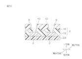
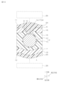
インダクタ1は、所定厚みを有し、略平板形状を有する。インダクタ1は、厚み方向に直交する第1方向に長い。インダクタ1は、平面視矩形状を有する。図2~図4に示すように、インダクタ1は、一方面11と、他方面12とを備える。一方面11は、他方面12に対して、厚み方向一方側に間隔を隔てて対向配置される。インダクタ1は、配線2と、磁性層3とを備える。
The
図1に示すように、配線2は、第1方向に沿って延びる。配線2の形状、寸法、構成、材料、処方(充填率、含有割合など)などは、例えば、特開2019-220618号公報などに記載される。図2~図3に示すように、配線2は、厚み方向および第2方向に沿う断面において、略円形状を有する。第2方向は、厚み方向および第1方向に直交する。配線2は、上記した断面において、外周面14を含む。配線2は、好ましくは、導体からなる導線4と、導線4の周面を被覆する絶縁膜5とを含む。
As shown in FIG. 1, the
磁性層3は、平面視において、インダクタ1と同一の外形形状を有する。磁性層3は、第1方向に延びるシート形状を有する。また、磁性層3は、断面視において、配線2を埋設する。磁性層3の材料は、バインダと、磁性粒子とを含む磁性組成物である。磁性粒子は、インダクタ1のインダクタンスを高める観点から、好ましくは、軟磁性粒子である。磁性組成物および磁性層3の形成方法は、例えば、特開2019-165221号公報、2019-165222号公報などに詳説される。磁性層3は、第1主面の一例としての第1主面6と、第2主面の一例としての第2主面7と、外側面8とを有する。
The
図2~図4に示すように、第1主面6は、磁性層3における厚み方向一方面を形成する。第1主面6は、インダクタ1の一方面11でもある。第1主面6は、配線2に対して厚み方向一方側に間隔を隔てて配置される。図2~図3に示すように、第1主面6は、配線2に対応する湾曲面を含む。
As shown in Figures 2 to 4, the first
第2主面7は、磁性層3における厚み方向他方面を形成する。第2主面7は、インダクタ1の他方面12でもある。第2主面7は、第1主面6の厚み方向他方側に間隔が隔てられる。第2主面7は、配線2に対して第1主面6の反対側に配置される。第2主面7は、配線2に対応する湾曲面を含む。
The second
図1~図2に示すように、外側面8は、磁性層3において、第2方向に間隔を隔てて対向する2つの側面である。外側面8は、第1主面6の第2方向両端縁のそれぞれと、第2主面7の両端縁のそれぞれとを連結する。
As shown in Figures 1 and 2, the
そして、図1~図3に示すように、磁性層3は、ビア10を有する。ビア10は、磁性層3において、配線2の第1方向両端部に対応して、設けられる。2つのビア10のそれぞれは、平面視略円形状を有する。ビア10は、インダクタ1の一方面11から配線2に向かって貫通する。ビア10は、絶縁膜5の厚み方向一方面34を露出する。厚み方向一方面34は、配線2の外周面14のうち、中心より厚み方向一方側に位置する部分である。ビア10は、内周面9と、底面17とを有する。
As shown in Figures 1 to 3, the
内周面9は、磁性層3において、ビア10の内部に臨む。内周面9は、図1に示すように、平面視(厚み方向から見たときと同義、以下同様。)において、無端形状である。具体的には、内周面9は、平面視略円環形状を有する。図2~図3に示すように、内周面9は、一方面11に近づくにつれて、ビア10の開口断面積が大きくなるテーパ面27を有する。具体的には、内周面9は、テーパ面27からなる。内周面9は、段差13を有する。段差13の数は、1つのビア10につき、例えば、1である。
The inner
底面17は、ビア10に臨む。底面17は、配線2の外周面14の一部である。また、底面17は、配線2の厚み方向一方面34でもある。底面17は、内周面9の厚み方向他方側の端縁(後述する第2端縁E2)に連続する。図1に示すように、底面17は、平面視略円形状を有する。また、底面17は、図2~図3に示すように、第2方向に沿う断面で、略円弧形状を有する。また、底面17は、図4に示すように、第1方向に沿う断面で、平坦形状である。底面17の最大高さ粗さRzは、例えば、10μm以下、好ましくは、1μm以下、より好ましくは、0.1μm以下であり、また、例えば、0.000001μm以上である。一方、被覆部18の最大高さ粗さRzは、例えば、10μm以下、好ましくは、1μm以下、より好ましくは、0.1μm以下であり、また、例えば、0.000001μm以上である。最大高さ粗さRzは、例えば、レーザー顕微鏡などで測定される。被覆部18は、厚み方向一方面34のうち、磁性層3に被覆される部分である。被覆部18の最大高さ粗さRzに対する、底面17の十点表面粗さRzの比は、例えば、2未満、好ましくは、1.5以下、より好ましくは、1.1以下であり、また、例えば、1以上である。比が上記した上限を下回れば、ビア10の底面17が被覆部18に対して過度に粗くなることが抑制される。そのため、導電部材19をビア10により一層確実に形成できる。
The
磁性層3は、単層または複層であってもよい。磁性層3が複層である場合には、例えば、配線2を埋設する第1層15と、2つの第2層16とを備える。2つの第2層16のそれぞれは、第1層15の厚み方向一方面および他方面のそれぞれに配置される。第2層16における磁性粒子の種類および/または割合は、第1層15のそれらと異なる。
The
そして、このインダクタ1では、溶融固化物Mの百分率は、10%以下である。
And in this
溶融固化物Mの百分率は、以下の方法によって求められる。 The percentage of molten solidified material M is determined by the following method:
まず、図2~図4に示すように、ビア10を横断する断面において、内周面9の厚み方向一方側の第1端縁E1を基準として第1主面6が延びる方向の一方側と他方側とにそれぞれ50μm離れて位置する第1点P1と第2点P2と、内周面9の厚み方向他方側の第2端縁E2を基準として延びる方向の一方側と他方側とにそれぞれ50μm離れて位置する第3点P3と第4点P4とを定める。
First, as shown in Figures 2 to 4, in a cross section across the via 10, a first point P1 and a second point P2 are defined, each located 50 μm apart on one side and the other side in the direction in which the first
ビア10を横断する断面は、図2および図3に示すように、第2方向に沿う断面であっても、図4に示すように、第1方向に沿う断面であってもよい。 The cross section across the via 10 may be a cross section along the second direction as shown in Figures 2 and 3, or a cross section along the first direction as shown in Figure 4.
第1端縁E1は、内周面9と第1主面6とによって形成される角である。第2方向に沿う断面において、第1主面6が延びる方向は、図2および図3に示すように、第1主面6が湾曲面であれば、第1端縁E1における接線方向である。一方、第1方向に沿う断面において、第1主面6が延びる方向は、図4に示すように、第1主面6が平坦面であれば、第1主面6に沿う方向であり、つまり、第1方向である。
The first edge E1 is an angle formed by the inner
第2端縁E2は、内周面9と、配線2の外周面14とによって形成される角である。第2端縁E2を基準として第3点P3と第4点P4とを定めるときの基準となる方向は、第1点P1と第2点P2とを定めるときの基準となる方向と同一である。そのため、第1点P1および第2点P2を結ぶ第1線分L1と、第3点P3および第4点P4を結ぶ第2線分L2とは、平行する。これにより、第1点P1と、第2点P2と、第3点P3と、第4点P4とを頂点となる四角形を形成する。四角形は、2辺(第1線分L1と第2線分L2と)が平行する四辺形であって、平行四辺形である。
The second edge E2 is an angle formed by the inner
続いて、四辺形の面積S0を取得する。 Next, obtain the area S0 of the quadrilateral.
続いて、四角形の内部に位置する溶融固化物Mの面積S1を取得する。溶融固化物Mは、後述する製造方法でビア10を形成するときに、図5に示すように、磁性粒子が溶融して凝集し、固化した固形物である。例えば、溶融固化物Mは、以下の通り定義することもできる。断面SEM画像観察によって、溶融していない磁性粒子10個について、外周を求め、平均値を算出する。また、断面SEM画像観察によって、溶融していない磁性粒子10個について、面積を求め、平均値を算出する。上記した磁性粒子の外周の平均値および面積の平均値よりそれぞれ大きい外周および面積を有する物が、溶融固化物である。 Next, the area S1 of the molten and solidified material M located inside the rectangle is obtained. The molten and solidified material M is a solid material formed when the via 10 is formed by the manufacturing method described below, as shown in FIG. 5, in which the magnetic particles melt, aggregate, and solidify. For example, the molten and solidified material M can also be defined as follows. The perimeters of 10 unmelted magnetic particles are obtained by observing cross-sectional SEM images, and the average value is calculated. The areas of 10 unmelted magnetic particles are also obtained by observing cross-sectional SEM images, and the average value is calculated. An object that has a perimeter and area larger than the average perimeter and area of the magnetic particles described above, respectively, is a molten and solidified material.
その後、四角形の面積S0に対する溶融固化物の面積S1の百分率(S1/S0×100)を求める。 Then, calculate the percentage of the area S1 of the molten solidified material relative to the area S0 of the rectangle (S1/S0 x 100).
図5に示すように、溶融固化物Mの百分率が10%超過であれば、溶融固化物Mによって、後述する導電部材19をビア10の内部に安定して形成できない。
As shown in FIG. 5, if the percentage of the molten solidified material M exceeds 10%, the molten solidified material M will not allow the
溶融固化物Mの百分率の上限は、好ましくは、7.5%、より好ましくは、5%、さらに好ましくは、2.5%、とりわけ好ましくは、1%、さらには、0.1%、さらには、0.01%が好適であり、最も好ましくは、溶融固化物Mの百分率が、0%である。 The upper limit of the percentage of the molten solidified material M is preferably 7.5%, more preferably 5%, even more preferably 2.5%, particularly preferably 1%, even more preferably 0.1%, and even more preferably 0.01%, and most preferably the percentage of the molten solidified material M is 0%.
インダクタ1の製造方法を、図6A~図6Dを参照して説明する。
The manufacturing method of
インダクタ1の製造方法は、第1工程と、第2工程とを備える。
The manufacturing method for
図6Aに示すように、第1工程では、磁性積層体20を作製する。磁性積層体20は、まだビア10が形成されていないインダクタ1である。磁性積層体20は、配線2と、磁性層3とを備える。磁性積層体20の作製方法は、例えば、特開2019-165221号公報、2019-165222号公報などに詳説される。
As shown in FIG. 6A, in the first step, a
図6B~図6Cに示すように、第2工程では、ビア10を磁性層3に形成する。ビア10の形成方法としては、例えば、ブラスト法が挙げられる。ブラスト法は、第3工程と、第4工程と、第5工程とを備える。
As shown in Figures 6B and 6C, in the second step, vias 10 are formed in the
図6Bに示すように、第3工程では、レジスト21を第1主面6に配置する。レジスト21は、ビア10に対応する開口部22を有する。開口部22は、レジスト21を厚み方向に貫通する。レジスト21は、次に説明する砥粒子との衝突によって損傷しにくい材料からなる。レジスト21の材料は、特に限定されない。レジスト21は、市販品を用いることができ、例えば、市販の「サンドブラスト用ドライフィルムレジスト」を用いることもできる。
As shown in FIG. 6B, in the third step, the resist 21 is placed on the first
図6Cに示すように、第4工程では、砥粒子を開口部22から露出する第1主面6に向けて噴射する。砥粒子の噴射では、砥粒子噴射装置(図示せず)が用いられる。
As shown in FIG. 6C, in the fourth step, abrasive particles are sprayed toward the first
砥粒子噴射装置は、図示しないが、例えば、導入部と、拡張部と、整流部と、集合部と、噴射ノズルとを、砥粒子の流れ方向に向かって順に備える。導入部は、砥粒子タンクおよびガスタンクに接続されている。拡張部は、砥粒子を内部で拡散させる。整流部は、砥粒子の流れを整える。集合部は、砥粒子をまとめながら、流動圧を上昇させる。噴射ノズルは、複数のノズルを備える。複数のノズルのそれぞれは、略円形状の孔である。噴射ノズルは、砥粒子を均等な状態で、複数のノズルから砥粒子を噴射する。砥粒子噴射装置の構成および使用条件等は、例えば、特開2015-199131号公報に記載される。砥粒子噴射装置は、市販品を用いることができる。 Although not shown, the abrasive particle injection device includes, for example, an introduction section, an expansion section, a flow straightening section, a collection section, and an injection nozzle, arranged in that order in the direction of the flow of the abrasive particles. The introduction section is connected to an abrasive particle tank and a gas tank. The expansion section diffuses the abrasive particles inside. The flow straightening section straightens the flow of the abrasive particles. The collection section increases the flow pressure while gathering the abrasive particles. The injection nozzle includes multiple nozzles. Each of the multiple nozzles is a substantially circular hole. The injection nozzle injects the abrasive particles from the multiple nozzles while keeping the abrasive particles uniform. The configuration and operating conditions of the abrasive particle injection device are described, for example, in JP 2015-199131 A. A commercially available product can be used as the abrasive particle injection device.
具体的には、砥粒子の材料としては、例えば、アルミナ、ガラスビーズ、炭化ケイ素、窒化ケイ素、ジルコニア、ステンレスなどが挙げられる。ノズル径は、例えば、0.1μm以上、好ましくは、0.5μm以上であり、また、例えば、10000μm以下、好ましくは、5000μm以下である。砥粒子のメジアン径は、例えば、0.1μm以上、好ましくは、0.5μm以上であり、また、例えば、1000μm以下、好ましくは、100μm以下である。砥粒子の噴射圧力は、例えば、0.01MPa以上、好ましくは、0.05MPa以上であり、また、例えば、10MPa以下、好ましくは、5MPa以下である。 Specific examples of materials for the abrasive particles include alumina, glass beads, silicon carbide, silicon nitride, zirconia, and stainless steel. The nozzle diameter is, for example, 0.1 μm or more, preferably 0.5 μm or more, and for example, 10,000 μm or less, preferably 5,000 μm or less. The median diameter of the abrasive particles is, for example, 0.1 μm or more, preferably 0.5 μm or more, and for example, 1,000 μm or less, preferably 100 μm or less. The spray pressure of the abrasive particles is, for example, 0.01 MPa or more, preferably 0.05 MPa or more, and for example, 10 MPa or less, preferably 5 MPa or less.
第4工程では、開口部22から露出する第1主面6が研削され、そして、ビア10が磁性層3に形成される。
In the fourth step, the first
図6Dに示すように、第5工程では、レジスト21を除去する。具体的には、レジスト21を第1主面6から剥離する。
As shown in FIG. 6D, in the fifth step, the resist 21 is removed. Specifically, the resist 21 is peeled off from the first
これによって、図2~図4に示すように、配線2と、磁性層3と、ビア10とを備えるインダクタ1が得られる。
This results in an
その後、図6Eに示すように、導電部材19を、例えば、めっき、具体的には、電解めっきなどによって、ビア10内に形成する。なお、導電部材19を形成する前に、ビア10における絶縁膜5を公知方法によって剥離する。絶縁膜5は、種々の方法で剥離でき、例えば、レーザー加工またはブラスト法で剥離できる。さらに、電解めっきの前に、シード層(図示せず)を形成する。また、導電部材19は、ビア10の底面17から析出する。また、導電部材19は、内周面9に沿って厚み方向に一方側に析出する。さらに、導電部材19は、ビア10の周囲の一方面11にも形成される。導電部材19の材料としては、例えば、銅などの導体が挙げられる。
Then, as shown in FIG. 6E, the
[第1実施形態の作用効果] [Effects of the first embodiment]
このインダクタ1では、溶融固化物の百分率が、10%以下と低いので、溶融固化物が少ない。そのため、図6Eに示すように、導電部材19を安定して形成できる。
In this
また、このインダクタ1では、内周面9は、第1主面6に近づくにつれて、ビア10の開口断面積が大きくなるテーパ面27を有するので、ビア10に導電部材19を充填すれば、導電部材19の厚み方向一方面の面積を大きくできる。そのため、外部機器との接続信頼性に優れる。
In addition, in this
図4に示すように、第1方向に沿う断面で、ビア10から露出する配線2の厚み方向一方面34は、平坦形状であるので、導電部材19を安定して形成できる。
As shown in FIG. 4, in a cross section along the first direction, one
図2~図4に示し、導電部材19を形成していないインダクタ1では、加工安定層24は、突出端部35の厚み方向一方面と内周面9とに配置されているので、それらに対する加工時の安定性を向上できる。一方、突出端部35は、導線4を被覆するので、導線4の劣化および損傷を抑制できる。
In the
また、磁性粒子が軟磁性粒子であれば、インダクタ1は、インダクタンスに優れる。
In addition, if the magnetic particles are soft magnetic particles, the
[第1実施形態の変形例] [Modification of the first embodiment]
内周面9における段差13の数は、0または複数であってもよい。段差13の数は、好ましくは、1以下であり、より好ましくは、0である。段差13の数が1以下であれば、導電部材19をより確実に安定して形成できる。図7には、段差13がない内周面9を描画する。
The number of
ビア10の形状は、平面視略円形状に限定されない。図8に示すように、例えば、ビア10は、平面視略矩形状を有する。この変形例では、ビア10は、平面視において、第1方向に長い。ビア10は、平面視において、最長長さD1と、最短長さD2とを有する。この変形例では、最長長さD1は、ビア10の矩形状において、対向する2つの頂点間の距離である。最短長さD2は、ビア10の第2方向長さである。最短長さD2に対する最長長さD1の比(D1/D2)の上限は、例えば、10、好ましくは、5、より好ましくは、3、さらに好ましくは、2である。比の下限は、例えば、1.1、好ましくは、1.2である。なお、図1に示すビア10の円形状では、最長長さD1と最短長さD2とが、同一である。比(D1/D2)が10以下と小さければ、ビア10に導電部材19を安定して形成できる。
The shape of the via 10 is not limited to a substantially circular shape in a plan view. As shown in FIG. 8, for example, the via 10 has a substantially rectangular shape in a plan view. In this modified example, the via 10 is long in the first direction in a plan view. The via 10 has a maximum length D1 and a minimum length D2 in a plan view. In this modified example, the maximum length D1 is the distance between two opposing vertices in the rectangular shape of the via 10. The minimum length D2 is the length of the via 10 in the second direction. The upper limit of the ratio (D1/D2) of the maximum length D1 to the minimum length D2 is, for example, 10, preferably 5, more preferably 3, and even more preferably 2. The lower limit of the ratio is, for example, 1.1, preferably 1.2. In the circular shape of the via 10 shown in FIG. 1, the maximum length D1 and the minimum length D2 are the same. If the ratio (D1/D2) is small, such as 10 or less, the
配線2の数は、複数でもよい。図9に示すように、配線2は、第2方向に間隔を隔てて対向配置される。複数(例えば、2つ)の配線2は、平面視で、平行する。ビア10は、配線2の数に対応して設けられる。
The number of
配線2の形状は、限定されない。図10に示すように、配線2の形状は、断面略矩形状であってもよい。
The shape of the
配線2の厚み方向他方面は、絶縁層23に接触する。絶縁層23は、第2方向に延びる。絶縁層23の材料としては、例えば、ポリイミドなどの、絶縁性の樹脂が挙げられる。
The other thickness-wise surface of the
第1実施形態では、インダクタ1の製造方法では、ブラスト法を用いたが、これに限定されない。好ましくは、ブラスト法が用いられる。ブラスト法であれば、溶融固化物Mの生成を可及的に低減できる。
In the first embodiment, the
別の変形例では、図11Aに示すように、内周面9は、テーパ面27と、第2テーパ面28とを有する。
In another modified example, as shown in FIG. 11A, the inner
テーパ面27は、一方面11に近づくにつれて、ビア10の開口断面積が大きくなる。テーパ面27は、第2端縁E2から厚み方向一方側に向かう。
The opening cross-sectional area of the via 10 increases as the tapered
一方、第2テーパ面28は、一方面11に近づくにつれて、ビア10の開口断面積が小さくなる。第2テーパ面28は、第1端縁E1からテーパ面27の厚み方向一端縁に至る。この内周面9では、テーパ面27と、第2テーパ面28とが、厚み方一方側に向かって順に配置される。
On the other hand, the opening cross-sectional area of the via 10 becomes smaller as the second tapered
第2方向において、2つの第2テーパ面28における厚み方向一端縁間の距離は、2つの第1端縁E1間の距離である。第2方向において、2つの第1端縁E1間の距離に対する、2つの第2テーパ面28における厚み方向他端縁E3間の距離の比は、例えば、1.1以上、好ましくは、1.2以上、より好ましくは、1.5以下であり、また、例えば、3以下である。
In the second direction, the distance between the first thickness-wise edges of the two second
第2方向において、2つの第2テーパ面28における厚み方向他端縁間の距離は、2つのE2間の距離である。第2方向において、2つの第2端縁E2間の距離に対する、2つの第2テーパ面28における厚み方向他端縁E3間の距離の比は、例えば、1.1以上、好ましくは、1.2以上、より好ましくは、1.5以下であり、また、例えば、3以下である。
In the second direction, the distance between the other thickness-wise edges of the two second
このビア10を作製するには、例えば、図6Bに示すレジスト21の開口部22を狭くする。具体的には、開口部22の直径が、例えば、300μm以下、好ましくは、200μm以下である。
To create this via 10, for example, the
すると、第4工程において、砥粒子は、狭い開口部22を通過して、磁性層3の第1主面6に衝突して、磁性層3を研削するが、砥粒子は、磁性層3において開口部22の周縁の厚み方向他方側において滞留し易い。この砥粒子は、噴射方向上流側に逆流する。このとき、砥粒子は、略円弧形状の軌道で、内周面9を形成する。そのため、砥粒子は、第2テーパ面28とテーパ面27とを有する内周面9を形成する。
In the fourth step, the abrasive particles pass through the
図11Bに示すように、導電部材19をビア10に設ければ、導電部材19は、テーパ面27と第2テーパ面28とに接触する。
As shown in FIG. 11B, when the
図11Bに示すように、このインダクタ1では、導電部材19をビア10に設けるときには、アンカー効果に基づき、導電部材19がビア10から脱落することを抑制できる。
As shown in FIG. 11B, in this
図12に示すように、内周面9は、テーパ面27を備えず、第2テーパ面28のみを備えることもできる。
As shown in FIG. 12, the inner
図示しないが、ビア10を、一方面11と他方面12との両方に設けることもできる。
Although not shown,
図示しないが、ビア10を、磁性層3において、配線2の第1方向一端部のみに設けることもできる。
Although not shown, the via 10 can also be provided in the
[第2実施形態] [Second embodiment]
第2実施形態において、上記した第1実施形態と同様の部材および工程については、同一の参照符号を付し、その詳細な説明を省略する。また、第2実施形態は、特記する以外、第1実施形態と同様の作用効果を奏することができる。さらに、第1実施形態および第2実施形態を適宜組み合わせることができる。 In the second embodiment, the same components and steps as those in the first embodiment described above are given the same reference numerals, and detailed descriptions thereof will be omitted. Furthermore, the second embodiment can achieve the same effects as the first embodiment, unless otherwise specified. Furthermore, the first and second embodiments can be combined as appropriate.
図13に示すように、このインダクタ1は、さらに、加工安定層24と第2加工安定層25とを備える。
As shown in FIG. 13, the
加工安定層24は、ビア10に充填されている。また、加工安定層24は、第1主面6にも配置されている。加工安定層24は、磁性層3の第1主面6に対する表面加工性と、ビア10の内周面9およびビア10に対する表面加工性とを向上させる。さらに、加工安定層24は、後述する貫通孔30に導電部材19を配置したとき(図14および第3実施形態参照)に、導電部材19と磁性層3との絶縁性を確保できる絶縁層でもある。
The
加工安定層24は、熱硬化性樹脂組成物の硬化物を含む。つまり、加工安定層24の材料は、熱硬化性樹脂組成物を含む。熱硬化性樹脂組成物は、熱硬化性樹脂を必須成分として含む。
The
熱硬化性樹脂は、主剤、硬化剤および硬化促進剤を含む。 Thermosetting resins contain a base resin, a curing agent and a curing accelerator.
主剤としては、例えば、エポキシ樹脂、シリコーン樹脂などが挙げられ、好ましくは、エポキシ樹脂が挙げられる。エポキシ樹脂としては、例えば、ビスフェノールA型エポキシ樹脂、ビスフェノールF型エポキシ樹脂、ビスフェノールS型エポキシ樹脂、変性ビスフェノールA型エポキシ樹脂、変性ビスフェノールF型エポキシ樹脂、変性ビスフェノールS型エポキシ樹脂、ビフェニル型エポキシ樹脂などの2官能エポキシ樹脂、例えば、フェノールノボラック型エポキシ樹脂、クレゾールノボラック型エポキシ樹脂、トリスヒドロキシフェニルメタン型エポキシ樹脂、テトラフェニロールエタン型エポキシ樹脂、ジシクロペンタジエン型エポキシ樹脂などの3官能以上の多官能エポキシ樹脂などが挙げられる。これらエポキシ樹脂は、単独で使用または2種以上を併用することができる。好ましくは、2官能エポキシ樹脂が挙げられ、より好ましくは、ビスフェノールA型エポキシ樹脂が挙げられる。 Examples of the base resin include epoxy resins and silicone resins, and preferably epoxy resins. Examples of the epoxy resin include bifunctional epoxy resins such as bisphenol A type epoxy resins, bisphenol F type epoxy resins, bisphenol S type epoxy resins, modified bisphenol A type epoxy resins, modified bisphenol F type epoxy resins, modified bisphenol S type epoxy resins, and biphenyl type epoxy resins, and polyfunctional epoxy resins having three or more functional groups such as phenol novolac type epoxy resins, cresol novolac type epoxy resins, trishydroxyphenylmethane type epoxy resins, tetraphenylolethane type epoxy resins, and dicyclopentadiene type epoxy resins. These epoxy resins can be used alone or in combination of two or more types. Preferably, bifunctional epoxy resins are used, and more preferably, bisphenol A type epoxy resins are used.
エポキシ樹脂のエポキシ当量の下限は、例えば、10g/eq.であり、また、上限は、例えば、1,000g/eq.である。 The lower limit of the epoxy equivalent of the epoxy resin is, for example, 10 g/eq., and the upper limit is, for example, 1,000 g/eq.
硬化剤としては、主剤がエポキシ樹脂であれば、フェノール樹脂、イソシアネート樹脂などが挙げられる。フェノール樹脂としては、例えば、フェノールノボラック樹脂、クレゾールノボラック樹脂、フェノールアラルキル樹脂、フェノールビフェニレン樹脂、ジシクロペンタジエン型フェノール樹脂、レゾール樹脂などの多官能フェノール樹脂が挙げられる。これらは、単独で使用または2種以上を併用することができる。フェノール樹脂として、好ましくは、フェノールノボラック樹脂、フェノールビフェニレン樹脂が挙げられる。主剤がエポキシ樹脂であり、硬化剤がフェノール樹脂であれば、エポキシ樹脂中のエポキシ基1当量に対して、フェノール樹脂中の水酸基の合計の下限が、例えば、0.7当量、好ましくは、0.9当量、また、上限が、例えば、1.5当量、好ましくは、1.2当量である。具体的には、硬化剤の質量部数の下限は、主剤100質量部に対して、例えば、1質量部であり、また、例えば、50質量部である。 If the main agent is an epoxy resin, the curing agent may be a phenolic resin or an isocyanate resin. Examples of the phenolic resin include polyfunctional phenolic resins such as phenolic novolac resin, cresol novolac resin, phenolic aralkyl resin, phenolic biphenylene resin, dicyclopentadiene type phenolic resin, and resol resin. These may be used alone or in combination of two or more. Examples of the phenolic resin include phenolic novolac resin and phenolic biphenylene resin. If the main agent is an epoxy resin and the curing agent is a phenolic resin, the lower limit of the total number of hydroxyl groups in the phenolic resin relative to 1 equivalent of epoxy groups in the epoxy resin is, for example, 0.7 equivalents, preferably 0.9 equivalents, and the upper limit is, for example, 1.5 equivalents, preferably 1.2 equivalents. Specifically, the lower limit of the number of parts by mass of the curing agent is, for example, 1 part by mass, or, for example, 50 parts by mass, relative to 100 parts by mass of the main agent.
硬化促進剤としては、主剤の硬化を促進する触媒(熱硬化触媒)(好ましくは、エポキシ樹脂硬化促進剤)であって、例えば、有機リン系化合物、例えば、2-フェニル-4-メチル-5-ヒドロキシメチルイミダゾール(2P4MHZ)などのイミダゾール化合物などが挙げられる。硬化促進剤の質量部数の下限は、主剤100質量部に対して、例えば、0.05質量部であり、また、上限が、例えば、5質量部である。 The curing accelerator is a catalyst (thermosetting catalyst) (preferably an epoxy resin curing accelerator) that accelerates the curing of the base agent, and examples of such accelerators include organophosphorus compounds, such as imidazole compounds such as 2-phenyl-4-methyl-5-hydroxymethylimidazole (2P4MHZ). The lower limit of the number of parts by mass of the curing accelerator is, for example, 0.05 parts by mass, and the upper limit is, for example, 5 parts by mass, per 100 parts by mass of the base agent.
さらに、熱硬化性樹脂組成物は、例えば、粒子を任意成分として含むことができる。粒子は、熱硬化性樹脂に分散されている。粒子は、例えば、第1粒子、および、第2粒子からなる群から選択される少なくとも1種類である。 Furthermore, the thermosetting resin composition may contain, for example, particles as an optional component. The particles are dispersed in the thermosetting resin. The particles are, for example, at least one type selected from the group consisting of first particles and second particles.
第1粒子は、例えば、略球形状を有する。第1粒子のメジアン径の下限は、例えば、1μm、好ましくは、5μmであり、また、第1粒子のメジアン径の上限は、例えば、250μm、好ましくは、200μmである。第1粒子のメジアン径は、レーザー回折式粒度分布測定装置で求められる。また、第1粒子のメジアン径は、例えば、断面観察による二値化処理によって、求めることもできる。 The first particles have, for example, a substantially spherical shape. The lower limit of the median diameter of the first particles is, for example, 1 μm, preferably 5 μm, and the upper limit of the median diameter of the first particles is, for example, 250 μm, preferably 200 μm. The median diameter of the first particles is determined using a laser diffraction particle size distribution measuring device. The median diameter of the first particles can also be determined, for example, by binarization processing based on cross-sectional observation.
第1粒子の材料は、特に限定されない。第1粒子の材料としては、例えば、金属類、無機化合物、有機化合物などが挙げられ、熱膨張係数を上げるために、好ましくは、金属類、無機化合物が挙げられる。 The material of the first particles is not particularly limited. Examples of materials for the first particles include metals, inorganic compounds, and organic compounds, and in order to increase the thermal expansion coefficient, metals and inorganic compounds are preferred.
金属類は、加工安定層24をインダンクタンス向上層として機能させる場合に熱硬化性樹脂組成物に含まれる。金属類としては、磁性層3で例示した磁性体が挙げられ、好ましくは、第1金属元素として鉄を含む有機鉄化合物、より好ましくは、カルボニル鉄が挙げられる。
Metals are included in the thermosetting resin composition when the
無機化合物は、加工安定層24を熱膨張係数抑制層として機能させる場合に熱硬化性樹脂組成物に含まれる。無機化合物としては、例えば、無機フィラーが挙げられ、具体的には、シリカ、アルミナなどが挙げられ、好ましくは、シリカが挙げられる。
The inorganic compound is included in the thermosetting resin composition when the
具体的には、第1粒子として、好ましくは、球形状シリカが挙げられ、また、好ましくは、球形状カルボニル鉄が挙げられる。 Specifically, the first particles are preferably spherical silica, and are preferably spherical carbonyl iron.
第2粒子は、例えば、略扁平形状を有する。略扁平形状は、略板形状を含む。 The second particles have, for example, a substantially flat shape. A substantially flat shape includes a substantially plate shape.
第2粒子の扁平率(扁平度)の下限は、例えば、8、好ましくは、15であり、また、上限は、例えば、500、好ましくは、450である。第2粒子の扁平率は、上記した磁性層3における磁性粒子の扁平率と同じ算出方法で求められる。
The lower limit of the flattening ratio (flatness) of the second particles is, for example, 8, preferably 15, and the upper limit is, for example, 500, preferably 450. The flattening ratio of the second particles is calculated using the same method as the flattening ratio of the magnetic particles in the
第2粒子のメジアン径の下限は、例えば、1μm、好ましくは、5μmであり、また、第2粒子のメジアン径の上限は、例えば、250μm、好ましくは、200μmである。第2粒子のメジアン径は、第1粒子のそれと同様の方法で求められる。 The lower limit of the median diameter of the second particles is, for example, 1 μm, preferably 5 μm, and the upper limit of the median diameter of the second particles is, for example, 250 μm, preferably 200 μm. The median diameter of the second particles is determined in the same manner as that of the first particles.
第2粒子の平均厚みの下限は、例えば、0.1μm、好ましくは、0.2μmであり、また、上限は、例えば、3.0μm、好ましくは、2.5μmである。 The lower limit of the average thickness of the second particles is, for example, 0.1 μm, preferably 0.2 μm, and the upper limit is, for example, 3.0 μm, preferably 2.5 μm.
第2粒子の材料は、例えば、無機化合物である。無機化合物としては、例えば、窒化ホウ素などの熱伝導性化合物などが挙げられる。従って、好ましくは、無機化合物は、加工安定層24を熱伝導性向上層として機能させる場合に熱硬化性樹脂組成物に含まれる。
The material of the second particles is, for example, an inorganic compound. Examples of inorganic compounds include thermally conductive compounds such as boron nitride. Therefore, preferably, the inorganic compound is included in the thermosetting resin composition when the
具体的には、第2粒子として、好ましくは、扁平形状の窒化ホウ素が挙げられる。 Specifically, the second particles are preferably flat-shaped boron nitride particles.
第1粒子および第2粒子は、熱硬化性樹脂組成物に、単独種類が含まれ、または、両方が含まれる。 The thermosetting resin composition may contain a single type of first particle and a second particle, or may contain both.
熱硬化性樹脂100質量部に対する粒子(第1粒子および/または第2粒子)の質量部数の下限は、例えば、10質量部、好ましくは、50質量部であり、また、上限は、例えば、2,000質量部、好ましくは、1,500質量部である。また、硬化物における粒子の含有割合の下限は、例えば、10質量%、また、上限は、例えば、90質量%である。第1粒子および第2粒子の両方が熱硬化性樹脂組成物に含まれる場合には、第1粒子100質量部に対する第2粒子の質量部数の下限は、例えば、30質量部、また、上限は、例えば、300質量部である。 The lower limit of the number of parts by mass of the particles (first particles and/or second particles) relative to 100 parts by mass of the thermosetting resin is, for example, 10 parts by mass, preferably 50 parts by mass, and the upper limit is, for example, 2,000 parts by mass, preferably 1,500 parts by mass. The lower limit of the particle content in the cured product is, for example, 10% by mass, and the upper limit is, for example, 90% by mass. When both the first particles and the second particles are included in the thermosetting resin composition, the lower limit of the number of parts by mass of the second particles relative to 100 parts by mass of the first particles is, for example, 30 parts by mass, and the upper limit is, for example, 300 parts by mass.
なお、粒子は、熱硬化性樹脂組成物における任意成分であることから、熱硬化性樹脂組成物が、粒子を含有しなくてもよい。 Note that since particles are an optional component in a thermosetting resin composition, the thermosetting resin composition does not have to contain particles.
一方、加工安定層24の材料は、熱可塑性樹脂をさらに含有してもよい。熱硬化性樹脂100質量部に対する熱可塑性樹脂の質量部数の下限は、例えば、1質量部、上限が、例えば、100質量部である。
On the other hand, the material of the
加工安定層24の厚みの下限は、例えば、1μm、好ましくは、10μmであり、また、上限は、例えば、1,000μm、好ましくは、100μmである。インダクタ1の厚みに対する加工安定層24の厚みの比の下限は、例えば、0.001、好ましくは、0.005、より好ましくは、0.01であり、また、上限は、例えば、0.5、好ましくは、0.3、より好ましくは、0.1である。なお、加工安定層24の厚みは、第1主面6と、加工安定層24の厚み方向一方面との間の最短長さである。
The lower limit of the thickness of the
第2加工安定層25は、インダクタ1の他方面12に配置されている。第2加工安定層25は、インダクタ1の他方面12に対する表面加工性を向上させる。第2加工安定層25は、熱硬化性樹脂組成物の硬化物を含んでおり、第2加工安定層25の材料は、加工安定層24で挙げられた熱硬化性樹脂組成物を含む。第2加工安定層25の厚みの下限は、例えば、1μm、好ましくは、10μmであり、また、上限は、例えば、1,000μm、好ましくは、100μmである。インダクタ1の厚みに対する第2加工安定層25の厚みの比の下限は、例えば、0.001、好ましくは、0.005、より好ましくは、0.01であり、また、上限は、例えば、0.5、好ましくは、0.3、より好ましくは、0.1である。なお、第2加工安定層25の厚みは、第2主面7と、第2加工安定層25の厚み方向他方面との間の最短長さである。
The second
第2実施形態のインダクタ1を得るには、図13の仮想線で示すように、2つの加工安定シート26を準備する。2つの加工安定シート26のそれぞれは、加工安定層24および第2加工安定層25の材料からシート形状に形成されている。加工安定シート26は、好ましくは、Bステージの熱硬化性樹脂組成物を含む。なお、上記した材料を、上記した熱硬化性樹脂組成物に、溶媒をさらに配合して、ワニスとして調製することもできる。さらに、材料には、熱可塑性樹脂をさらに配合することもできる。この方法では、ワニスを図示しない剥離シートの表面に塗布および乾燥させて、加工安定シート26を形成する。
To obtain the
続いて、2つの加工安定シート26およびインダクタ1を、厚み方向両側からプレスする。その後、それらを加熱して、2つの加工安定シート26をCステージ化する。これによって、磁性層3の第1主面6とビア10の内周面9と絶縁膜5の厚み方向一方面34とに配置される加工安定層24と、磁性層3の第2主面7に配置される第2加工安定層25とが、インダクタ1に備えられる。
Next, the two
[第2実施形態の作用効果] [Effects of the second embodiment]
第2実施形態のインダクタ1では、加工安定層24が、ビア10に充填されるので、ビア10に対する次の加工(後述の第3実施形態)時の安定性を向上できる。
In the
[第3実施形態] [Third embodiment]
第3実施形態において、上記した第1~第2実施形態と同様の部材および工程については、同一の参照符号を付し、その詳細な説明を省略する。また、第3実施形態は、特記する以外、第1~第2実施形態と同様の作用効果を奏することができる。さらに、第1実施形態~第3実施形態を適宜組み合わせることができる。 In the third embodiment, the same components and steps as those in the first and second embodiments described above are given the same reference numerals, and detailed descriptions thereof will be omitted. Furthermore, the third embodiment can achieve the same effects as the first and second embodiments, unless otherwise specified. Furthermore, the first to third embodiments can be combined as appropriate.
図14に示すように、導線4の厚み方向一方面34は、厚み方向一方側に露出する。例えば、導線4の厚み方向一方面34は、加工安定層24と、絶縁膜5の一部とから露出する。
As shown in FIG. 14, one
加工安定層24は、第1被覆部31と、第2被覆部32とを備える。第1被覆部31は、第1主面6に追従してそれを被覆する。第1被覆部31は、第1主面6の厚み方向一方面に位置する。第2被覆部32は、ビア10の内周面9に追従してそれを被覆する。第2被覆部32は、第2方向(または第1方向)に投影したときに、内周面9と重複する。また、第2被覆部32は、厚み方向に沿う。第2被覆部32の厚み方向他端面は、絶縁膜5の突出端部35に、厚み方向一方側から接触する。第2被覆部32の厚み方向他端面は、第2被覆部32において第1被覆部31に対する反対側に位置する面である。突出端部35は、絶縁膜5の一部である。突出端部35は、平面視略円環形状を有する。なお、突出端部35の円環形状は、図14において描画されていない。突出端部35は、その内側において、導線4の厚み方向一方面34の一部を露出する。突出端部35の内側面と、第2被覆部32の内側面とは、面一である。
The
これによって、絶縁膜5の突出端部35と、加工安定層24の第2被覆部32とは、導線4の厚み方向一方面34を厚み方向一方側に向かって露出する。
As a result, the protruding
ビア10は、加工安定層24の第2被覆部32と、絶縁膜5の突出端部35と、導線4の厚み方向一方面34とによって区画される。
The via 10 is defined by the
ビア10を形成するには、第2実施形態の加工安定層24を、例えば、穿孔加工する。穿孔加工としては、例えば、レーザー加工などが挙げられる。
To form the via 10, the
[第3実施形態の作用効果] [Effects of the third embodiment]
このインダクタ1では、導線4の厚み方向一方面34が、第2被覆部32と突出端部35とから露出しているので、導電部材19を一方面34に設ければ、導線4を外部機器と電気的に接続できる。
In this
一方、加工安定層24が絶縁層であれば、加工安定層24が、導電部材19と磁性層3との間に介在できるので、それらの絶縁性を向上できる。
On the other hand, if the
以下に実施例および比較例を示し、本発明をさらに具体的に説明する。なお、本発明は、何ら実施例および比較例に限定されない。また、以下の記載において用いられる配合割合(含有割合)、物性値、パラメータなどの具体的数値は、上記の「発明を実施するための形態」において記載されている、それらに対応する配合割合(含有割合)、物性値、パラメータなど該当記載の上限(「以下」、「未満」として定義されている数値)または下限(「以上」、「超過」として定義されている数値)に代替することができる。 The present invention will be described in more detail below with reference to examples and comparative examples. Note that the present invention is in no way limited to the examples and comparative examples. Furthermore, the specific numerical values of the blending ratio (content ratio), physical property values, parameters, etc. used in the following description can be replaced with the upper limit (a numerical value defined as "equal to or less than") or lower limit (a numerical value defined as "equal to or more than" or "exceeding") of the corresponding blending ratio (content ratio), physical property value, parameter, etc. described in the above "Form for carrying out the invention".
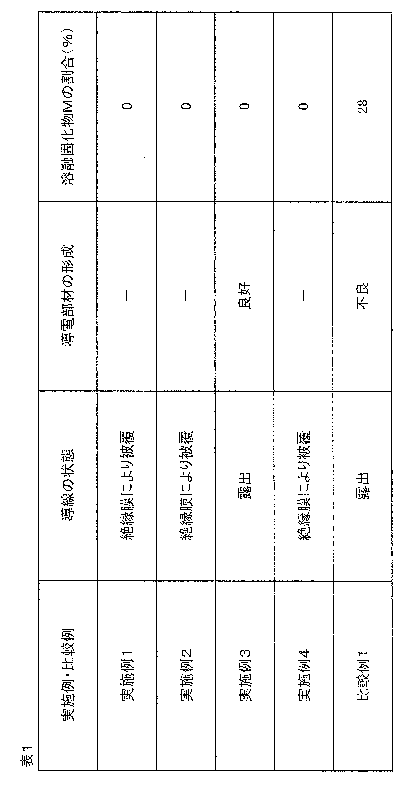
実施例1
[第1実施形態に対応する実施例]
Example 1
[Example corresponding to the first embodiment]
図6Aに示すように、まず、磁性積層体20を作製した。具体的には、半径115μmの複数の配線2を、厚み100μmの第1磁性シートと、厚み125μmの第2磁性シートとからなる磁性層3で被覆した。なお、第1磁性シートは、球状磁性粉61.5体積%、クレゾールノボラック型エポキシ樹脂(主剤)9.6体積%、フェノール樹脂(硬化剤)9.6体積%、ポリエーテルリン酸エステル(分散剤)0.5体積%、イミダゾール化合物(硬化促進剤)0.3体積%、および、熱可塑性樹脂(カルボキシル基含有アクリル酸エステルコポリマー)18.5体積%を含む。また、第2磁性シートは、扁平形状のFe-Si合金からなる磁性粒子を55体積%、クレゾールノボラック型エポキシ樹脂(主剤)11.0体積%、フェノール樹脂(硬化剤)11.0体積%、ポリエーテルリン酸エステル(分散剤)0.4体積%、イミダゾール化合物(硬化促進剤)0.4体積%、および、熱可塑性樹脂(カルボキシル基含有アクリル酸エステルコポリマー)21.2体積%を含む。
As shown in FIG. 6A, first, a
図6Bに示すように、レジスト21を、絶縁膜5の第1主面6に形成した。レジスト21に、フォトリソ工程を経て、開口部22を形成する。開口部22は、平面視円形状であった。開口部22の直径は、250μmであった。
As shown in FIG. 6B, a resist 21 was formed on the first
図6Cに示すように、ブラスト法で、ビア10を形成した。ビア10の内周面9は、テーパ面27を有する。
As shown in FIG. 6C, the via 10 was formed by a blasting method. The inner
ブラスト法の条件を以下に記載する。 The conditions for the blasting method are listed below.
ノズル径:2mm
砥粒子の材料:アルミナ
砥粒子のメジアン径:14μm
噴射速度:0.4MPa
Nozzle diameter: 2 mm
Abrasive grain material: Alumina Abrasive grain median diameter: 14 μm
Injection speed: 0.4MPa
続いて、図6Dに示すように、レジスト21を第1主面6から剥離した。
Next, as shown in FIG. 6D, the resist 21 was peeled off from the first
これによって、インダクタ1を製造した。
This resulted in the production of
実施例2
[第2実施形態に対応する実施例]
図13に示すように、実施例1のインダクタ1に、加工安定層24と第2加工安定層25とを備えた。
Example 2
[Example corresponding to the second embodiment]
As shown in FIG. 13, the
具体的には、まず、図13の仮想線で示すように、2つの加工安定シート26を準備した。加工安定シート26は、球形状のシリカ粒子(第1粒子)935質量部、ビスフェノールA型エポキシ樹脂(熱硬化性樹脂の主剤)100質量部、フェノール樹脂(硬化剤)106質量部、イミダゾール化合物(硬化促進剤)4質量部、および、および、シクロへキノン(溶媒)10質量部を含むワニスの塗布および乾燥によって形成される。加工安定シート26におけるシリカ粒子の含有割合は、55体積%である。加工安定シート26の厚みは、40μmである。加工安定シート26は、Bステージである。
Specifically, first, two
2つの加工安定シート26およびインダクタ1を厚み方向両側からプレスした。その後、加工安定シート26をCステージ化した。
The two
実施例3
[第3実施形態に対応する実施例]
図14に示すように、実施例2の加工安定層24にビア10を形成した。
Example 3
[Example corresponding to the third embodiment]
As shown in FIG. 14, a via 10 was formed in the
具体的には、レーザー装置を用いて、加工安定層24にビア10を形成した。
Specifically, a via 10 was formed in the
その後、図6Eに示すように、ビア10に無電解銅めっきによりシード層(図示せず)を形成した後、導電部材19を電解銅めっきにより形成した。導電部材19は、円滑に形成できた。
After that, as shown in FIG. 6E, a seed layer (not shown) was formed in the via 10 by electroless copper plating, and then the
実施例4
開口部22の直径を100μmに変更した以外は、実施例1と同様に処理した。図11Aに示すように、内周面9は、テーパ面27と、第2テーパ面28とを有していた。
Example 4
Except for changing the diameter of the
なお、第2方向において、2つの第1端縁E1間の距離が105μm、2つの第2端縁E2間の距離が85μm、2つの第2テーパ面28における厚み方向他端縁E3間の距離が122μmであった。
In addition, in the second direction, the distance between the two first edges E1 was 105 μm, the distance between the two second edges E2 was 85 μm, and the distance between the other edges E3 in the thickness direction of the two second
比較例1
ブラスト法に代え、レーザー加工に変更した以外は、実施例1と同様に処理した。導線4は、レーザー加工によって、露出した。さらに、導電部材19を電解銅めっきにより形成しようと試みた。しかし、導電部材19の形成に不良が生じた。
Comparative Example 1
Except for changing the blasting method to laser processing, the treatment was the same as in Example 1. The
評価
SEM観察、溶融固化物Mの割合および導電部材の形成
Evaluation: SEM observation, proportion of molten solidified material M, and formation of conductive material
各実施例~比較例の断面SEM観察を実施した。実施例1の第2方向に沿うSEMの画像処理図を図3に示す。比較例1の第1方向に沿うSEMの画像処理図を図5に示す。 Cross-sectional SEM observations were performed for each of the Examples and Comparative Examples. Figure 3 shows a processed SEM image along the second direction for Example 1. Figure 5 shows a processed SEM image along the first direction for Comparative Example 1.
併せて、溶融固化物Mの百分率を求めた。その結果を表1に示す。 The percentage of molten solidified material M was also calculated. The results are shown in Table 1.
また、断面SEM画像から、ビア10の底面17と内周面17における導電部材19を観察し、以下の基準で、導電部材19の形成を評価した。
In addition, the
[良好] 導電部材19が溶融固化物Mを介して形成されていなかった。
[不良] 導電部材19が溶融固化物Mを介して形成されていた。
[Good] The
[Defective] The
1 インダクタ
2 配線
3 磁性層
4 導線
4 配線
5 絶縁膜
6 第1主面
7 第2主面
9 内周面
10 ビア
11 一方面
13 段差
24 加工安定層
27 テーパ面
28 第2テーパ面
34 方向一方面
34 一方面
35 突出端部
M 溶融固化物
P1 第1点
P2 第2点
P3 第3点
P4 第4点
E1 第1端縁
E2 第2端縁
Claims (10)
前記配線を埋設し、磁性粒子を含有する磁性層とを備えるインダクタであって、
前記磁性層は、
前記配線に対して厚み方向一方側に間隔を隔てて配置される第1主面と、
前記第1主面と厚み方向に間隔を隔てられ、前記配線に対して前記第1主面の反対側に配置される第2主面と、
前記第1主面から前記配線に向かって貫通するビアとを有し、
前記ビアは、厚み方向から見たときに無端形状である内周面を有し、
1つの前記ビアにおいて、前記内周面は、段差を有し、
下記の方法によって求められる溶融固化物の百分率が、10%以下であることを特徴とする、インダクタ。
前記ビアを横断する断面において、前記内周面の厚み方向一方側の端縁を基準として前記第1主面が延びる方向の一方側と他方側とにそれぞれ50μm離れて位置する第1点と第2点と、前記内周面の厚み方向他方側の端縁を基準として前記延びる方向の一方側と他方側とにそれぞれ50μm離れて位置する第3点と第4点とを頂点とする四角形の面積S0を取得する。前記四角形の内部に位置する前記溶融固化物の面積S1を取得する。前記四角形の前記面積S0に対する前記溶融固化物の前記面積S1の百分率(S1/S0×100)を求める。 Wiring and
a magnetic layer having the wiring embedded therein and containing magnetic particles,
The magnetic layer is
A first main surface disposed on one side in a thickness direction with a gap therebetween with respect to the wiring;
a second main surface that is spaced apart from the first main surface in a thickness direction and is disposed on an opposite side of the first main surface with respect to the wiring;
a via penetrating from the first main surface toward the wiring,
The via has an inner circumferential surface that is endless when viewed in a thickness direction,
In one of the vias, the inner circumferential surface has a step,
An inductor, characterized in that a percentage of molten solidified matter determined by the following method is 10% or less.
In a cross section across the via, an area S0 of a rectangle is obtained, the area S0 being defined by vertices being a first point and a second point located 50 μm apart on one side and the other side in the direction in which the first main surface extends, with respect to an edge on one side in the thickness direction of the inner circumferential surface, and a third point and a fourth point located 50 μm apart on one side and the other side in the direction in which the first main surface extends, with respect to an edge on the other side in the thickness direction of the inner circumferential surface. An area S1 of the molten solidified material located inside the rectangle is obtained. The percentage (S1/S0×100) of the area S1 of the molten solidified material relative to the area S0 of the rectangle is calculated.
前記絶縁膜は、前記ビアから露出していることを特徴とする、請求項1~4のいずれか一項に記載のインダクタ。 The wiring includes a conductive wire and an insulating film disposed on a peripheral surface of the conductive wire,
5. The inductor according to claim 1 , wherein the insulating film is exposed from the via.
前記絶縁膜は、前記ビアにおいて、前記内周面の他端縁から内側に突出する突出端部を有し、
前記突出端部の厚み方向一方面と前記内周面とに配置される加工安定層をさらに備え、
前記突出端部と前記加工安定層とは、前記導線の厚み方向一方面を露出していることを特徴とする、請求項1~4のいずれか一項に記載のインダクタ。 The wiring includes a conductive wire and an insulating film disposed on a peripheral surface of the conductive wire,
the insulating film has a protruding end portion protruding inward from the other end edge of the inner circumferential surface of the via;
Further, a processing stabilizing layer is provided on one surface in the thickness direction of the protruding end portion and on the inner peripheral surface,
5. The inductor according to claim 1, wherein the protruding end and the processing stability layer expose one surface of the conductor in a thickness direction.
前記最短長さD2に対する前記最長長さD1の比(D1/D2)が、10以下であることを特徴とする、請求項1~9のいずれか一項に記載のインダクタ。 The via has a maximum length D1 and a minimum length D2 in a planar direction perpendicular to the thickness direction,
10. The inductor according to claim 1 , wherein a ratio (D1/D2) of the longest length D1 to the shortest length D2 is 10 or less.
Priority Applications (5)
| Application Number | Priority Date | Filing Date | Title |
|---|---|---|---|
| JP2020126344A JP7546397B2 (en) | 2020-07-27 | 2020-07-27 | Inductors |
| KR1020210093884A KR20220013912A (en) | 2020-07-27 | 2021-07-19 | Inductor |
| US17/381,745 US12444532B2 (en) | 2020-07-27 | 2021-07-21 | Inductor |
| CN202110836587.XA CN113990603B (en) | 2020-07-27 | 2021-07-23 | Inductor(s) |
| TW110127338A TW202205318A (en) | 2020-07-27 | 2021-07-26 | Inductor |
Applications Claiming Priority (1)
| Application Number | Priority Date | Filing Date | Title |
|---|---|---|---|
| JP2020126344A JP7546397B2 (en) | 2020-07-27 | 2020-07-27 | Inductors |
Publications (2)
| Publication Number | Publication Date |
|---|---|
| JP2022023413A JP2022023413A (en) | 2022-02-08 |
| JP7546397B2 true JP7546397B2 (en) | 2024-09-06 |
Family
ID=79688626
Family Applications (1)
| Application Number | Title | Priority Date | Filing Date |
|---|---|---|---|
| JP2020126344A Active JP7546397B2 (en) | 2020-07-27 | 2020-07-27 | Inductors |
Country Status (5)
| Country | Link |
|---|---|
| US (1) | US12444532B2 (en) |
| JP (1) | JP7546397B2 (en) |
| KR (1) | KR20220013912A (en) |
| CN (1) | CN113990603B (en) |
| TW (1) | TW202205318A (en) |
Citations (7)
| Publication number | Priority date | Publication date | Assignee | Title |
|---|---|---|---|---|
| US20100265030A1 (en) | 2009-04-17 | 2010-10-21 | Nxp B.V. | Inductive components for dc/dc converters and methods of manufacture thereof |
| JP2015088753A (en) | 2013-10-29 | 2015-05-07 | サムソン エレクトロ−メカニックス カンパニーリミテッド. | COIL COMPONENT AND METHOD FOR MANUFACTURING THE SAME, COIL COMPONENT SUBSTRATE, AND VOLTAGE CONTROL MODULE INCLUDING THE SAME |
| JP2017098544A (en) | 2015-11-20 | 2017-06-01 | サムソン エレクトロ−メカニックス カンパニーリミテッド. | Coil parts |
| JP2017112130A (en) | 2015-12-14 | 2017-06-22 | 株式会社村田製作所 | Electronic component and method for manufacturing the same |
| JP2017216401A (en) | 2016-06-01 | 2017-12-07 | 株式会社村田製作所 | Electronic component |
| JP2019160929A (en) | 2018-03-09 | 2019-09-19 | 日東電工株式会社 | Wiring board and manufacturing method of the same |
| JP2020088285A (en) | 2018-11-29 | 2020-06-04 | 味の素株式会社 | Substrate manufacturing method |
Family Cites Families (12)
| Publication number | Priority date | Publication date | Assignee | Title |
|---|---|---|---|---|
| JP3197022B2 (en) * | 1991-05-13 | 2001-08-13 | ティーディーケイ株式会社 | Multilayer ceramic parts for noise suppressor |
| US7161089B2 (en) * | 2002-12-04 | 2007-01-09 | Tdk Corporation | Electronic component |
| JP6062691B2 (en) | 2012-04-25 | 2017-01-18 | Necトーキン株式会社 | Sheet-shaped inductor, multilayer substrate built-in type inductor, and manufacturing method thereof |
| JP2014078546A (en) | 2012-10-09 | 2014-05-01 | Panasonic Corp | Manufacturing method of multilayer inductor |
| JP2015199131A (en) | 2014-04-04 | 2015-11-12 | 株式会社アルプスエンジニアリング | Abrasive material injection device |
| JP6413654B2 (en) | 2014-11-04 | 2018-10-31 | 味の素株式会社 | Circuit board and manufacturing method thereof |
| KR102450597B1 (en) * | 2017-09-29 | 2022-10-07 | 삼성전기주식회사 | Coil component and method for manufacturing the same |
| JP7372747B2 (en) | 2018-03-16 | 2023-11-01 | 日東電工株式会社 | Wired circuit board and its manufacturing method |
| JP7352363B2 (en) | 2018-03-16 | 2023-09-28 | 日東電工株式会社 | Magnetic wiring circuit board and its manufacturing method |
| JP7220948B2 (en) | 2018-04-09 | 2023-02-13 | 日東電工株式会社 | magnetic wiring circuit board |
| JP7223525B2 (en) * | 2018-08-09 | 2023-02-16 | 新光電気工業株式会社 | Inductor and inductor manufacturing method |
| KR102662847B1 (en) * | 2019-09-30 | 2024-05-03 | 삼성전기주식회사 | Printed circuit board |
-
2020
- 2020-07-27 JP JP2020126344A patent/JP7546397B2/en active Active
-
2021
- 2021-07-19 KR KR1020210093884A patent/KR20220013912A/en active Pending
- 2021-07-21 US US17/381,745 patent/US12444532B2/en active Active
- 2021-07-23 CN CN202110836587.XA patent/CN113990603B/en active Active
- 2021-07-26 TW TW110127338A patent/TW202205318A/en unknown
Patent Citations (7)
| Publication number | Priority date | Publication date | Assignee | Title |
|---|---|---|---|---|
| US20100265030A1 (en) | 2009-04-17 | 2010-10-21 | Nxp B.V. | Inductive components for dc/dc converters and methods of manufacture thereof |
| JP2015088753A (en) | 2013-10-29 | 2015-05-07 | サムソン エレクトロ−メカニックス カンパニーリミテッド. | COIL COMPONENT AND METHOD FOR MANUFACTURING THE SAME, COIL COMPONENT SUBSTRATE, AND VOLTAGE CONTROL MODULE INCLUDING THE SAME |
| JP2017098544A (en) | 2015-11-20 | 2017-06-01 | サムソン エレクトロ−メカニックス カンパニーリミテッド. | Coil parts |
| JP2017112130A (en) | 2015-12-14 | 2017-06-22 | 株式会社村田製作所 | Electronic component and method for manufacturing the same |
| JP2017216401A (en) | 2016-06-01 | 2017-12-07 | 株式会社村田製作所 | Electronic component |
| JP2019160929A (en) | 2018-03-09 | 2019-09-19 | 日東電工株式会社 | Wiring board and manufacturing method of the same |
| JP2020088285A (en) | 2018-11-29 | 2020-06-04 | 味の素株式会社 | Substrate manufacturing method |
Also Published As
| Publication number | Publication date |
|---|---|
| TW202205318A (en) | 2022-02-01 |
| US20220028599A1 (en) | 2022-01-27 |
| CN113990603A (en) | 2022-01-28 |
| KR20220013912A (en) | 2022-02-04 |
| US12444532B2 (en) | 2025-10-14 |
| CN113990603B (en) | 2026-02-13 |
| JP2022023413A (en) | 2022-02-08 |
Similar Documents
| Publication | Publication Date | Title |
|---|---|---|
| EP1986200B1 (en) | Composite magnetic sheet and process for producing the same | |
| KR100918339B1 (en) | Dielectric filler-containing resin for forming a built-in capacitor layer of a printed wiring board, and a double-sided copper clad laminate in which a dielectric layer is formed using the dielectric filler-containing resin, and a method of manufacturing the double-sided copper clad laminate | |
| KR100832628B1 (en) | Conductive paste | |
| JP7565721B2 (en) | How to manufacture an inductor | |
| US7083859B2 (en) | Conductive powder and method for preparing the same | |
| WO2002035554A1 (en) | Electroconductive metal paste and method for production thereof | |
| KR100685273B1 (en) | Insulation material, film, circuit board and manufacturing method thereof | |
| CN111937501A (en) | Curable resin composition, cured product thereof, and printed circuit board | |
| JP4235888B2 (en) | Conductive paste | |
| KR20190092404A (en) | Package Substrate and Manufacturing Method of Package Substrate | |
| WO2004027787A1 (en) | Conductive composition for electrical connection of electronic device and electronic device | |
| TW202100342A (en) | Conductive adhesive sheet | |
| TWI847061B (en) | Electromagnetic wave shielding film and shielding printed wiring board | |
| JP7546397B2 (en) | Inductors | |
| JP5344097B2 (en) | Semiconductor sealing film-like resin composition, semiconductor device manufacturing method, and semiconductor device | |
| JP5609492B2 (en) | Electronic component and manufacturing method thereof | |
| JP2022060975A (en) | Inductor and method for manufacturing inductor | |
| JP2011228481A (en) | Conductive paste, flexible printed-wiring board and electronic equipment | |
| JP2022060995A (en) | Soft magnetic powder and inductor | |
| JP7069967B2 (en) | Heat dissipation board | |
| JP6006539B2 (en) | Circuit board and electronic component mounting board | |
| JP2021086912A (en) | Electronic component mounting board and electronic device | |
| JP2004127537A (en) | Conductive thermosetting resin composition for electrode formation | |
| JP2001302884A (en) | Electrodonductive paste | |
| WO2023190423A1 (en) | Conductive adhesive layer and heat dissipation structure |
Legal Events
| Date | Code | Title | Description |
|---|---|---|---|
| A621 | Written request for application examination |
Free format text: JAPANESE INTERMEDIATE CODE: A621 Effective date: 20230601 |
|
| A131 | Notification of reasons for refusal |
Free format text: JAPANESE INTERMEDIATE CODE: A131 Effective date: 20240109 |
|
| A977 | Report on retrieval |
Free format text: JAPANESE INTERMEDIATE CODE: A971007 Effective date: 20240111 |
|
| A601 | Written request for extension of time |
Free format text: JAPANESE INTERMEDIATE CODE: A601 Effective date: 20240304 |
|
| A521 | Request for written amendment filed |
Free format text: JAPANESE INTERMEDIATE CODE: A523 Effective date: 20240423 |
|
| A131 | Notification of reasons for refusal |
Free format text: JAPANESE INTERMEDIATE CODE: A131 Effective date: 20240521 |
|
| A521 | Request for written amendment filed |
Free format text: JAPANESE INTERMEDIATE CODE: A523 Effective date: 20240719 |
|
| TRDD | Decision of grant or rejection written | ||
| A01 | Written decision to grant a patent or to grant a registration (utility model) |
Free format text: JAPANESE INTERMEDIATE CODE: A01 Effective date: 20240806 |
|
| A61 | First payment of annual fees (during grant procedure) |
Free format text: JAPANESE INTERMEDIATE CODE: A61 Effective date: 20240827 |
|
| R150 | Certificate of patent or registration of utility model |
Ref document number: 7546397 Country of ref document: JP Free format text: JAPANESE INTERMEDIATE CODE: R150 |