JP7367777B2 - ショットキーバリアダイオード - Google Patents
ショットキーバリアダイオード Download PDFInfo
- Publication number
- JP7367777B2 JP7367777B2 JP2021571084A JP2021571084A JP7367777B2 JP 7367777 B2 JP7367777 B2 JP 7367777B2 JP 2021571084 A JP2021571084 A JP 2021571084A JP 2021571084 A JP2021571084 A JP 2021571084A JP 7367777 B2 JP7367777 B2 JP 7367777B2
- Authority
- JP
- Japan
- Prior art keywords
- guard ring
- semiconductor substrate
- schottky barrier
- inner guard
- barrier diode
- Prior art date
- Legal status (The legal status is an assumption and is not a legal conclusion. Google has not performed a legal analysis and makes no representation as to the accuracy of the status listed.)
- Active
Links
- 230000004888 barrier function Effects 0.000 title claims description 65
- 239000004065 semiconductor Substances 0.000 claims description 114
- 239000000758 substrate Substances 0.000 claims description 59
- 239000013078 crystal Substances 0.000 claims description 7
- 230000007547 defect Effects 0.000 claims description 7
- AJNVQOSZGJRYEI-UHFFFAOYSA-N digallium;oxygen(2-) Chemical compound [O-2].[O-2].[O-2].[Ga+3].[Ga+3] AJNVQOSZGJRYEI-UHFFFAOYSA-N 0.000 claims description 3
- 229910001195 gallium oxide Inorganic materials 0.000 claims description 3
- HBMJWWWQQXIZIP-UHFFFAOYSA-N silicon carbide Chemical group [Si+]#[C-] HBMJWWWQQXIZIP-UHFFFAOYSA-N 0.000 claims description 3
- 229910010271 silicon carbide Inorganic materials 0.000 claims description 3
- 229910002601 GaN Inorganic materials 0.000 claims description 2
- JMASRVWKEDWRBT-UHFFFAOYSA-N Gallium nitride Chemical compound [Ga]#N JMASRVWKEDWRBT-UHFFFAOYSA-N 0.000 claims description 2
- 239000010432 diamond Substances 0.000 claims description 2
- 229910003460 diamond Inorganic materials 0.000 claims description 2
- 239000000463 material Substances 0.000 claims description 2
- 229910021420 polycrystalline silicon Inorganic materials 0.000 claims description 2
- 229920005591 polysilicon Polymers 0.000 claims description 2
- 230000015556 catabolic process Effects 0.000 description 5
- BOTDANWDWHJENH-UHFFFAOYSA-N Tetraethyl orthosilicate Chemical compound CCO[Si](OCC)(OCC)OCC BOTDANWDWHJENH-UHFFFAOYSA-N 0.000 description 2
- 239000012141 concentrate Substances 0.000 description 2
- 230000008878 coupling Effects 0.000 description 2
- 238000010168 coupling process Methods 0.000 description 2
- 238000005859 coupling reaction Methods 0.000 description 2
- 230000006378 damage Effects 0.000 description 2
- 238000010586 diagram Methods 0.000 description 2
- 229910052710 silicon Inorganic materials 0.000 description 2
- 239000010703 silicon Substances 0.000 description 2
- 108091006146 Channels Proteins 0.000 description 1
- 108010075750 P-Type Calcium Channels Proteins 0.000 description 1
- 230000015572 biosynthetic process Effects 0.000 description 1
- 230000000052 comparative effect Effects 0.000 description 1
- 230000000694 effects Effects 0.000 description 1
- 230000005684 electric field Effects 0.000 description 1
- 238000010894 electron beam technology Methods 0.000 description 1
- 239000012535 impurity Substances 0.000 description 1
- 150000002500 ions Chemical class 0.000 description 1
- 238000004519 manufacturing process Methods 0.000 description 1
- 229910052751 metal Inorganic materials 0.000 description 1
- 239000002184 metal Substances 0.000 description 1
- 230000004048 modification Effects 0.000 description 1
- 238000012986 modification Methods 0.000 description 1
- 238000010992 reflux Methods 0.000 description 1
Images


Classifications
-
- H—ELECTRICITY
- H01—ELECTRIC ELEMENTS
- H01L—SEMICONDUCTOR DEVICES NOT COVERED BY CLASS H10
- H01L29/00—Semiconductor devices specially adapted for rectifying, amplifying, oscillating or switching and having potential barriers; Capacitors or resistors having potential barriers, e.g. a PN-junction depletion layer or carrier concentration layer; Details of semiconductor bodies or of electrodes thereof ; Multistep manufacturing processes therefor
- H01L29/40—Electrodes ; Multistep manufacturing processes therefor
- H01L29/43—Electrodes ; Multistep manufacturing processes therefor characterised by the materials of which they are formed
- H01L29/47—Schottky barrier electrodes
-
- H—ELECTRICITY
- H01—ELECTRIC ELEMENTS
- H01L—SEMICONDUCTOR DEVICES NOT COVERED BY CLASS H10
- H01L29/00—Semiconductor devices specially adapted for rectifying, amplifying, oscillating or switching and having potential barriers; Capacitors or resistors having potential barriers, e.g. a PN-junction depletion layer or carrier concentration layer; Details of semiconductor bodies or of electrodes thereof ; Multistep manufacturing processes therefor
- H01L29/66—Types of semiconductor device ; Multistep manufacturing processes therefor
- H01L29/86—Types of semiconductor device ; Multistep manufacturing processes therefor controllable only by variation of the electric current supplied, or only the electric potential applied, to one or more of the electrodes carrying the current to be rectified, amplified, oscillated or switched
- H01L29/861—Diodes
- H01L29/872—Schottky diodes
-
- H—ELECTRICITY
- H01—ELECTRIC ELEMENTS
- H01L—SEMICONDUCTOR DEVICES NOT COVERED BY CLASS H10
- H01L29/00—Semiconductor devices specially adapted for rectifying, amplifying, oscillating or switching and having potential barriers; Capacitors or resistors having potential barriers, e.g. a PN-junction depletion layer or carrier concentration layer; Details of semiconductor bodies or of electrodes thereof ; Multistep manufacturing processes therefor
- H01L29/02—Semiconductor bodies ; Multistep manufacturing processes therefor
- H01L29/06—Semiconductor bodies ; Multistep manufacturing processes therefor characterised by their shape; characterised by the shapes, relative sizes, or dispositions of the semiconductor regions ; characterised by the concentration or distribution of impurities within semiconductor regions
- H01L29/0603—Semiconductor bodies ; Multistep manufacturing processes therefor characterised by their shape; characterised by the shapes, relative sizes, or dispositions of the semiconductor regions ; characterised by the concentration or distribution of impurities within semiconductor regions characterised by particular constructional design considerations, e.g. for preventing surface leakage, for controlling electric field concentration or for internal isolations regions
- H01L29/0642—Isolation within the component, i.e. internal isolation
- H01L29/0646—PN junctions
-
- H—ELECTRICITY
- H01—ELECTRIC ELEMENTS
- H01L—SEMICONDUCTOR DEVICES NOT COVERED BY CLASS H10
- H01L29/00—Semiconductor devices specially adapted for rectifying, amplifying, oscillating or switching and having potential barriers; Capacitors or resistors having potential barriers, e.g. a PN-junction depletion layer or carrier concentration layer; Details of semiconductor bodies or of electrodes thereof ; Multistep manufacturing processes therefor
- H01L29/02—Semiconductor bodies ; Multistep manufacturing processes therefor
- H01L29/30—Semiconductor bodies ; Multistep manufacturing processes therefor characterised by physical imperfections; having polished or roughened surface
- H01L29/32—Semiconductor bodies ; Multistep manufacturing processes therefor characterised by physical imperfections; having polished or roughened surface the imperfections being within the semiconductor body
-
- H—ELECTRICITY
- H01—ELECTRIC ELEMENTS
- H01L—SEMICONDUCTOR DEVICES NOT COVERED BY CLASS H10
- H01L29/00—Semiconductor devices specially adapted for rectifying, amplifying, oscillating or switching and having potential barriers; Capacitors or resistors having potential barriers, e.g. a PN-junction depletion layer or carrier concentration layer; Details of semiconductor bodies or of electrodes thereof ; Multistep manufacturing processes therefor
- H01L29/40—Electrodes ; Multistep manufacturing processes therefor
- H01L29/41—Electrodes ; Multistep manufacturing processes therefor characterised by their shape, relative sizes or dispositions
- H01L29/417—Electrodes ; Multistep manufacturing processes therefor characterised by their shape, relative sizes or dispositions carrying the current to be rectified, amplified or switched
-
- H—ELECTRICITY
- H01—ELECTRIC ELEMENTS
- H01L—SEMICONDUCTOR DEVICES NOT COVERED BY CLASS H10
- H01L29/00—Semiconductor devices specially adapted for rectifying, amplifying, oscillating or switching and having potential barriers; Capacitors or resistors having potential barriers, e.g. a PN-junction depletion layer or carrier concentration layer; Details of semiconductor bodies or of electrodes thereof ; Multistep manufacturing processes therefor
- H01L29/66—Types of semiconductor device ; Multistep manufacturing processes therefor
- H01L29/66007—Multistep manufacturing processes
- H01L29/66075—Multistep manufacturing processes of devices having semiconductor bodies comprising group 14 or group 13/15 materials
- H01L29/66083—Multistep manufacturing processes of devices having semiconductor bodies comprising group 14 or group 13/15 materials the devices being controllable only by variation of the electric current supplied or the electric potential applied, to one or more of the electrodes carrying the current to be rectified, amplified, oscillated or switched, e.g. two-terminal devices
- H01L29/6609—Diodes
- H01L29/66143—Schottky diodes
-
- H—ELECTRICITY
- H01—ELECTRIC ELEMENTS
- H01L—SEMICONDUCTOR DEVICES NOT COVERED BY CLASS H10
- H01L29/00—Semiconductor devices specially adapted for rectifying, amplifying, oscillating or switching and having potential barriers; Capacitors or resistors having potential barriers, e.g. a PN-junction depletion layer or carrier concentration layer; Details of semiconductor bodies or of electrodes thereof ; Multistep manufacturing processes therefor
- H01L29/02—Semiconductor bodies ; Multistep manufacturing processes therefor
- H01L29/06—Semiconductor bodies ; Multistep manufacturing processes therefor characterised by their shape; characterised by the shapes, relative sizes, or dispositions of the semiconductor regions ; characterised by the concentration or distribution of impurities within semiconductor regions
- H01L29/0603—Semiconductor bodies ; Multistep manufacturing processes therefor characterised by their shape; characterised by the shapes, relative sizes, or dispositions of the semiconductor regions ; characterised by the concentration or distribution of impurities within semiconductor regions characterised by particular constructional design considerations, e.g. for preventing surface leakage, for controlling electric field concentration or for internal isolations regions
- H01L29/0607—Semiconductor bodies ; Multistep manufacturing processes therefor characterised by their shape; characterised by the shapes, relative sizes, or dispositions of the semiconductor regions ; characterised by the concentration or distribution of impurities within semiconductor regions characterised by particular constructional design considerations, e.g. for preventing surface leakage, for controlling electric field concentration or for internal isolations regions for preventing surface leakage or controlling electric field concentration
- H01L29/0611—Semiconductor bodies ; Multistep manufacturing processes therefor characterised by their shape; characterised by the shapes, relative sizes, or dispositions of the semiconductor regions ; characterised by the concentration or distribution of impurities within semiconductor regions characterised by particular constructional design considerations, e.g. for preventing surface leakage, for controlling electric field concentration or for internal isolations regions for preventing surface leakage or controlling electric field concentration for increasing or controlling the breakdown voltage of reverse biased devices
- H01L29/0615—Semiconductor bodies ; Multistep manufacturing processes therefor characterised by their shape; characterised by the shapes, relative sizes, or dispositions of the semiconductor regions ; characterised by the concentration or distribution of impurities within semiconductor regions characterised by particular constructional design considerations, e.g. for preventing surface leakage, for controlling electric field concentration or for internal isolations regions for preventing surface leakage or controlling electric field concentration for increasing or controlling the breakdown voltage of reverse biased devices by the doping profile or the shape or the arrangement of the PN junction, or with supplementary regions, e.g. junction termination extension [JTE]
- H01L29/0619—Semiconductor bodies ; Multistep manufacturing processes therefor characterised by their shape; characterised by the shapes, relative sizes, or dispositions of the semiconductor regions ; characterised by the concentration or distribution of impurities within semiconductor regions characterised by particular constructional design considerations, e.g. for preventing surface leakage, for controlling electric field concentration or for internal isolations regions for preventing surface leakage or controlling electric field concentration for increasing or controlling the breakdown voltage of reverse biased devices by the doping profile or the shape or the arrangement of the PN junction, or with supplementary regions, e.g. junction termination extension [JTE] with a supplementary region doped oppositely to or in rectifying contact with the semiconductor containing or contacting region, e.g. guard rings with PN or Schottky junction
-
- H—ELECTRICITY
- H01—ELECTRIC ELEMENTS
- H01L—SEMICONDUCTOR DEVICES NOT COVERED BY CLASS H10
- H01L29/00—Semiconductor devices specially adapted for rectifying, amplifying, oscillating or switching and having potential barriers; Capacitors or resistors having potential barriers, e.g. a PN-junction depletion layer or carrier concentration layer; Details of semiconductor bodies or of electrodes thereof ; Multistep manufacturing processes therefor
- H01L29/02—Semiconductor bodies ; Multistep manufacturing processes therefor
- H01L29/12—Semiconductor bodies ; Multistep manufacturing processes therefor characterised by the materials of which they are formed
- H01L29/16—Semiconductor bodies ; Multistep manufacturing processes therefor characterised by the materials of which they are formed including, apart from doping materials or other impurities, only elements of Group IV of the Periodic Table
- H01L29/1608—Silicon carbide
-
- H—ELECTRICITY
- H01—ELECTRIC ELEMENTS
- H01L—SEMICONDUCTOR DEVICES NOT COVERED BY CLASS H10
- H01L29/00—Semiconductor devices specially adapted for rectifying, amplifying, oscillating or switching and having potential barriers; Capacitors or resistors having potential barriers, e.g. a PN-junction depletion layer or carrier concentration layer; Details of semiconductor bodies or of electrodes thereof ; Multistep manufacturing processes therefor
- H01L29/40—Electrodes ; Multistep manufacturing processes therefor
- H01L29/402—Field plates
Landscapes
- Engineering & Computer Science (AREA)
- Microelectronics & Electronic Packaging (AREA)
- Power Engineering (AREA)
- Physics & Mathematics (AREA)
- Ceramic Engineering (AREA)
- Condensed Matter Physics & Semiconductors (AREA)
- General Physics & Mathematics (AREA)
- Computer Hardware Design (AREA)
- Manufacturing & Machinery (AREA)
- Electrodes Of Semiconductors (AREA)
Description
本開示に係るショットキーバリアダイオードは、n型の半導体基板と、該半導体基板の上面側に設けられた少なくとも1つのp型のガードリングと、該少なくとも1つのガードリングのうち最も内側の内側ガードリングの上に設けられた絶縁膜と、該半導体基板の上面に設けられ、該絶縁膜の上に乗り上げたアノード電極と、該半導体基板の裏面に設けられたカソード電極と、該内側ガードリングよりも高抵抗であり、該内側ガードリングと該アノード電極とを隔てる高抵抗層と、を備え、該高抵抗層は、該内側ガードリングよりも低濃度の第1p型半導体層を有し、該半導体基板の上面側のうち該内側ガードリングよりも内側で該内側ガードリングと接触して設けられ、該絶縁膜は、該内側ガードリングの上面を全て覆い、該第1p型半導体層は、該絶縁膜から露出する。
図1は、実施の形態1に係るショットキーバリアダイオード100の断面図である。ショットキーバリアダイオード100は、半導体基板10を備える。半導体基板10は例えばシリコンから形成される。半導体基板10は、n+型半導体層12とn+型半導体層12の上に設けられたn型半導体層14を備える。
図3は、実施の形態2に係るショットキーバリアダイオード200の断面図である。ショットキーバリアダイオード200は絶縁膜20の形状がショットキーバリアダイオード100と異なる。実施の形態1において、絶縁膜20の内側の端部は直角形状であった。これに対し、本実施の形態に係る絶縁膜20の端部のうち半導体基板10の内側に設けられた側は、テーパー状である。
図4は、実施の形態3に係るショットキーバリアダイオード300の断面図である。ショットキーバリアダイオード300は、カソード電極330の構造がショットキーバリアダイオード100と異なる。カソード電極330には、内側ガードリング17の直下に半導体基板10を露出させる開口部332が形成される。
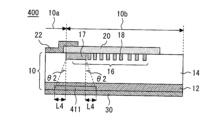
図5は、実施の形態4に係るショットキーバリアダイオード400の断面図である。ショットキーバリアダイオード400は、第2p型半導体層411を備える点がショットキーバリアダイオード100と異なる。第2p型半導体層411は、半導体基板10のうち、内側ガードリング17の直下に設けられる。第2p型半導体層411は、半導体基板10の裏面側に設けられる。
図6は、実施の形態5に係るショットキーバリアダイオード500の断面図である。ショットキーバリアダイオード500は、結晶欠陥層519を備える点がショットキーバリアダイオード100と異なる。結晶欠陥層519は、半導体基板10のうち内側ガードリング17の直下に設けられる。結晶欠陥層519は、イオン照射、電子線照射等により形成される。
図7は、実施の形態6に係るショットキーバリアダイオード600の断面図である。ショットキーバリアダイオード600は、第1p型半導体層615を備える点がショットキーバリアダイオード100と異なる。第1p型半導体層615は、半導体基板10の上面側のうち内側ガードリング17よりも内側で、内側ガードリング17と接触して設けられる。第1p型半導体層615は、内側ガードリング17よりも低濃度である。内側ガードリング17と第1p型半導体層615は電気的に接続され、同電位である。
図8は、実施の形態7に係るショットキーバリアダイオード700の断面図である。本実施の形態では、絶縁膜20の配置と、抵抗体724を備える点がショットキーバリアダイオード100と異なる。絶縁膜20は、内側ガードリング17の一部を除き複数のガードリング16を被覆する。内側ガードリング17は、端部のうち半導体基板10の内側に設けられた側に絶縁膜20から露出した露出部を有する。抵抗体724は露出部を覆う。
Claims (12)
- n型の半導体基板と、
前記半導体基板の上面側に設けられた少なくとも1つのp型のガードリングと、
前記少なくとも1つのガードリングのうち最も内側の内側ガードリングの上に設けられた絶縁膜と、
前記半導体基板の上面に設けられ、前記絶縁膜の上に乗り上げたアノード電極と、
前記半導体基板の裏面に設けられたカソード電極と、
前記内側ガードリングよりも高抵抗であり、前記内側ガードリングと前記アノード電極とを隔てる高抵抗層と、
を備え、
前記高抵抗層は、前記半導体基板の上面のうち前記絶縁膜よりも内側に設けられた抵抗体を有し、
前記内側ガードリングは、端部のうち前記半導体基板の内側に設けられた側に前記絶縁膜から露出した露出部を有し、
前記抵抗体は前記露出部を覆うことを特徴とするショットキーバリアダイオード。 - n型の半導体基板と、
前記半導体基板の上面側に設けられた少なくとも1つのp型のガードリングと、
前記少なくとも1つのガードリングのうち最も内側の内側ガードリングの上に設けられた絶縁膜と、
前記半導体基板の上面に設けられ、前記絶縁膜の上に乗り上げたアノード電極と、
前記半導体基板の裏面に設けられたカソード電極と、
前記内側ガードリングよりも高抵抗であり、前記内側ガードリングと前記アノード電極とを隔てる高抵抗層と、
を備え、
前記高抵抗層は、前記内側ガードリングよりも低濃度の第1p型半導体層を有し、前記半導体基板の上面側のうち前記内側ガードリングよりも内側で前記内側ガードリングと接触して設けられ、
前記絶縁膜は、前記内側ガードリングの上面を全て覆い、
前記第1p型半導体層は、前記絶縁膜から露出することを特徴とするショットキーバリアダイオード。 - 前記抵抗体はポリシリコン抵抗体であることを特徴とする請求項1に記載のショットキーバリアダイオード。
- 前記アノード電極は、端部が前記内側ガードリングの直上に設けられることを特徴とする請求項1から3の何れか1項に記載のショットキーバリアダイオード。
- 前記絶縁膜の厚さは1.0μm以上であることを特徴とする請求項1から4の何れか1項に記載のショットキーバリアダイオード。
- 前記カソード電極には、前記内側ガードリングの直下に前記半導体基板を露出させる開口部が形成されることを特徴とする請求項1から5の何れか1項に記載のショットキーバリアダイオード。
- 前記開口部は、前記内側ガードリングの直下から一定の範囲で前記半導体基板を露出させることを特徴とする請求項6に記載のショットキーバリアダイオード。
- 前記半導体基板のうち前記内側ガードリングの直下に設けられた第2p型半導体層を備えることを特徴とする請求項1から7の何れか1項に記載のショットキーバリアダイオード。
- 前記第2p型半導体層は、前記内側ガードリングの直下から一定の範囲まで設けられることを特徴とする請求項8に記載のショットキーバリアダイオード。
- 前記半導体基板のうち前記内側ガードリングの直下に設けられた結晶欠陥層を備えることを特徴とする請求項1から9の何れか1項に記載のショットキーバリアダイオード。
- 前記半導体基板はワイドバンドギャップ半導体によって形成されていることを特徴とする請求項1から10の何れか1項に記載のショットキーバリアダイオード。
- 前記ワイドバンドギャップ半導体は、炭化珪素、酸化ガリウム、窒化ガリウム系材料またはダイヤモンドであることを特徴とする請求項11に記載のショットキーバリアダイオード。
Applications Claiming Priority (1)
| Application Number | Priority Date | Filing Date | Title |
|---|---|---|---|
| PCT/JP2020/000900 WO2021144851A1 (ja) | 2020-01-14 | 2020-01-14 | ショットキーバリアダイオード |
Publications (2)
| Publication Number | Publication Date |
|---|---|
| JPWO2021144851A1 JPWO2021144851A1 (ja) | 2021-07-22 |
| JP7367777B2 true JP7367777B2 (ja) | 2023-10-24 |
Family
ID=76863985
Family Applications (1)
| Application Number | Title | Priority Date | Filing Date |
|---|---|---|---|
| JP2021571084A Active JP7367777B2 (ja) | 2020-01-14 | 2020-01-14 | ショットキーバリアダイオード |
Country Status (5)
| Country | Link |
|---|---|
| US (1) | US20220376073A1 (ja) |
| JP (1) | JP7367777B2 (ja) |
| CN (1) | CN114930546A (ja) |
| DE (1) | DE112020006511T5 (ja) |
| WO (1) | WO2021144851A1 (ja) |
Families Citing this family (1)
| Publication number | Priority date | Publication date | Assignee | Title |
|---|---|---|---|---|
| WO2024005153A1 (ja) * | 2022-06-29 | 2024-01-04 | 株式会社Flosfia | 半導体装置および半導体装置の製造方法 |
Citations (4)
| Publication number | Priority date | Publication date | Assignee | Title |
|---|---|---|---|---|
| JP2004022743A (ja) | 2002-06-14 | 2004-01-22 | Sanken Electric Co Ltd | ショットキバリアを有する半導体装置 |
| JP2006228772A (ja) | 2005-02-15 | 2006-08-31 | Matsushita Electric Ind Co Ltd | ショットキバリアダイオードとその製造方法 |
| WO2014192444A1 (ja) | 2013-05-29 | 2014-12-04 | 住友電気工業株式会社 | 半導体装置 |
| JP2015065469A (ja) | 2010-03-08 | 2015-04-09 | クリー インコーポレイテッドCree Inc. | ヘテロ接合障壁領域を含む半導体デバイス及びその製造方法 |
Family Cites Families (1)
| Publication number | Priority date | Publication date | Assignee | Title |
|---|---|---|---|---|
| JPS59232467A (ja) * | 1983-06-16 | 1984-12-27 | Toshiba Corp | ガ−ドリング付きシヨツトキ−バリヤ−ダイオ−ド |
-
2020
- 2020-01-14 JP JP2021571084A patent/JP7367777B2/ja active Active
- 2020-01-14 US US17/774,080 patent/US20220376073A1/en active Pending
- 2020-01-14 DE DE112020006511.1T patent/DE112020006511T5/de active Pending
- 2020-01-14 WO PCT/JP2020/000900 patent/WO2021144851A1/ja active Application Filing
- 2020-01-14 CN CN202080092316.1A patent/CN114930546A/zh active Pending
Patent Citations (4)
| Publication number | Priority date | Publication date | Assignee | Title |
|---|---|---|---|---|
| JP2004022743A (ja) | 2002-06-14 | 2004-01-22 | Sanken Electric Co Ltd | ショットキバリアを有する半導体装置 |
| JP2006228772A (ja) | 2005-02-15 | 2006-08-31 | Matsushita Electric Ind Co Ltd | ショットキバリアダイオードとその製造方法 |
| JP2015065469A (ja) | 2010-03-08 | 2015-04-09 | クリー インコーポレイテッドCree Inc. | ヘテロ接合障壁領域を含む半導体デバイス及びその製造方法 |
| WO2014192444A1 (ja) | 2013-05-29 | 2014-12-04 | 住友電気工業株式会社 | 半導体装置 |
Also Published As
| Publication number | Publication date |
|---|---|
| US20220376073A1 (en) | 2022-11-24 |
| DE112020006511T5 (de) | 2022-11-17 |
| JPWO2021144851A1 (ja) | 2021-07-22 |
| WO2021144851A1 (ja) | 2021-07-22 |
| CN114930546A (zh) | 2022-08-19 |
Similar Documents
| Publication | Publication Date | Title |
|---|---|---|
| JP5517688B2 (ja) | 半導体装置 | |
| US10714603B2 (en) | Semiconductor device | |
| JP6801324B2 (ja) | 半導体装置 | |
| US9147758B2 (en) | Semiconductor device | |
| JP5863574B2 (ja) | 半導体装置 | |
| US20160351657A1 (en) | Semiconductor apparatus | |
| US20170077217A1 (en) | Semiconductor device | |
| JP2015162610A (ja) | 半導体装置 | |
| JP2019140138A (ja) | 半導体素子およびその製造方法 | |
| US10204980B2 (en) | Semiconductor device and manufacturing method of the same | |
| JP6730237B2 (ja) | 半導体装置 | |
| JP7367777B2 (ja) | ショットキーバリアダイオード | |
| JP2012033802A (ja) | 半導体装置 | |
| JP5865860B2 (ja) | 半導体装置 | |
| US20200328301A1 (en) | Silicon carbide semiconductor device | |
| JP7188230B2 (ja) | 半導体装置 | |
| JP5607120B2 (ja) | 炭化珪素ショットキダイオード | |
| JP2016207829A (ja) | 絶縁ゲート型スイッチング素子 | |
| JP2016162776A (ja) | 半導体装置 | |
| EP3010045A1 (en) | Semiconductor device and a method of manufacturing same | |
| JP2014204067A (ja) | 半導体装置およびその製造方法 | |
| JP5656889B2 (ja) | 半導体装置及びこれを備えた半導体モジュール | |
| JP5358141B2 (ja) | 半導体装置 | |
| JP6058712B2 (ja) | 半導体装置 | |
| JP5774744B2 (ja) | 半導体装置 |
Legal Events
| Date | Code | Title | Description |
|---|---|---|---|
| A621 | Written request for application examination |
Free format text: JAPANESE INTERMEDIATE CODE: A621 Effective date: 20220414 |
|
| A131 | Notification of reasons for refusal |
Free format text: JAPANESE INTERMEDIATE CODE: A131 Effective date: 20230516 |
|
| A521 | Request for written amendment filed |
Free format text: JAPANESE INTERMEDIATE CODE: A523 Effective date: 20230607 |
|
| TRDD | Decision of grant or rejection written | ||
| A01 | Written decision to grant a patent or to grant a registration (utility model) |
Free format text: JAPANESE INTERMEDIATE CODE: A01 Effective date: 20230912 |
|
| A61 | First payment of annual fees (during grant procedure) |
Free format text: JAPANESE INTERMEDIATE CODE: A61 Effective date: 20230925 |
|
| R150 | Certificate of patent or registration of utility model |
Ref document number: 7367777 Country of ref document: JP Free format text: JAPANESE INTERMEDIATE CODE: R150 |