JP7345397B2 - 基板支持装置 - Google Patents
基板支持装置 Download PDFInfo
- Publication number
- JP7345397B2 JP7345397B2 JP2019559270A JP2019559270A JP7345397B2 JP 7345397 B2 JP7345397 B2 JP 7345397B2 JP 2019559270 A JP2019559270 A JP 2019559270A JP 2019559270 A JP2019559270 A JP 2019559270A JP 7345397 B2 JP7345397 B2 JP 7345397B2
- Authority
- JP
- Japan
- Prior art keywords
- substrate
- coating layer
- support member
- temperature compensation
- temperature
- Prior art date
- Legal status (The legal status is an assumption and is not a legal conclusion. Google has not performed a legal analysis and makes no representation as to the accuracy of the status listed.)
- Active
Links
Images

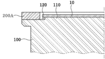

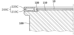


Classifications
-
- H—ELECTRICITY
- H01—ELECTRIC ELEMENTS
- H01J—ELECTRIC DISCHARGE TUBES OR DISCHARGE LAMPS
- H01J37/00—Discharge tubes with provision for introducing objects or material to be exposed to the discharge, e.g. for the purpose of examination or processing thereof
- H01J37/32—Gas-filled discharge tubes
- H01J37/32431—Constructional details of the reactor
- H01J37/32715—Workpiece holder
- H01J37/32724—Temperature
-
- H—ELECTRICITY
- H10—SEMICONDUCTOR DEVICES; ELECTRIC SOLID-STATE DEVICES NOT OTHERWISE PROVIDED FOR
- H10P—GENERIC PROCESSES OR APPARATUS FOR THE MANUFACTURE OR TREATMENT OF DEVICES COVERED BY CLASS H10
- H10P72/00—Handling or holding of wafers, substrates or devices during manufacture or treatment thereof
- H10P72/70—Handling or holding of wafers, substrates or devices during manufacture or treatment thereof for supporting or gripping
- H10P72/76—Handling or holding of wafers, substrates or devices during manufacture or treatment thereof for supporting or gripping using mechanical means, e.g. clamps or pinches
- H10P72/7604—Handling or holding of wafers, substrates or devices during manufacture or treatment thereof for supporting or gripping using mechanical means, e.g. clamps or pinches the wafers being placed on a susceptor, stage or support
- H10P72/7616—Handling or holding of wafers, substrates or devices during manufacture or treatment thereof for supporting or gripping using mechanical means, e.g. clamps or pinches the wafers being placed on a susceptor, stage or support characterised by a coating, a hardness or a material
-
- H—ELECTRICITY
- H10—SEMICONDUCTOR DEVICES; ELECTRIC SOLID-STATE DEVICES NOT OTHERWISE PROVIDED FOR
- H10P—GENERIC PROCESSES OR APPARATUS FOR THE MANUFACTURE OR TREATMENT OF DEVICES COVERED BY CLASS H10
- H10P72/00—Handling or holding of wafers, substrates or devices during manufacture or treatment thereof
- H10P72/04—Apparatus for manufacture or treatment
- H10P72/0431—Apparatus for thermal treatment
-
- H—ELECTRICITY
- H10—SEMICONDUCTOR DEVICES; ELECTRIC SOLID-STATE DEVICES NOT OTHERWISE PROVIDED FOR
- H10P—GENERIC PROCESSES OR APPARATUS FOR THE MANUFACTURE OR TREATMENT OF DEVICES COVERED BY CLASS H10
- H10P72/00—Handling or holding of wafers, substrates or devices during manufacture or treatment thereof
- H10P72/06—Apparatus for monitoring, sorting, marking, testing or measuring
- H10P72/0602—Temperature monitoring
-
- H—ELECTRICITY
- H10—SEMICONDUCTOR DEVICES; ELECTRIC SOLID-STATE DEVICES NOT OTHERWISE PROVIDED FOR
- H10P—GENERIC PROCESSES OR APPARATUS FOR THE MANUFACTURE OR TREATMENT OF DEVICES COVERED BY CLASS H10
- H10P72/00—Handling or holding of wafers, substrates or devices during manufacture or treatment thereof
- H10P72/70—Handling or holding of wafers, substrates or devices during manufacture or treatment thereof for supporting or gripping
- H10P72/76—Handling or holding of wafers, substrates or devices during manufacture or treatment thereof for supporting or gripping using mechanical means, e.g. clamps or pinches
- H10P72/7604—Handling or holding of wafers, substrates or devices during manufacture or treatment thereof for supporting or gripping using mechanical means, e.g. clamps or pinches the wafers being placed on a susceptor, stage or support
- H10P72/7611—Handling or holding of wafers, substrates or devices during manufacture or treatment thereof for supporting or gripping using mechanical means, e.g. clamps or pinches the wafers being placed on a susceptor, stage or support characterised by edge profile or support profile
-
- H—ELECTRICITY
- H10—SEMICONDUCTOR DEVICES; ELECTRIC SOLID-STATE DEVICES NOT OTHERWISE PROVIDED FOR
- H10P—GENERIC PROCESSES OR APPARATUS FOR THE MANUFACTURE OR TREATMENT OF DEVICES COVERED BY CLASS H10
- H10P72/00—Handling or holding of wafers, substrates or devices during manufacture or treatment thereof
- H10P72/70—Handling or holding of wafers, substrates or devices during manufacture or treatment thereof for supporting or gripping
- H10P72/76—Handling or holding of wafers, substrates or devices during manufacture or treatment thereof for supporting or gripping using mechanical means, e.g. clamps or pinches
- H10P72/7604—Handling or holding of wafers, substrates or devices during manufacture or treatment thereof for supporting or gripping using mechanical means, e.g. clamps or pinches the wafers being placed on a susceptor, stage or support
- H10P72/7621—Handling or holding of wafers, substrates or devices during manufacture or treatment thereof for supporting or gripping using mechanical means, e.g. clamps or pinches the wafers being placed on a susceptor, stage or support characterised by supporting two or more semiconductor substrates
-
- H—ELECTRICITY
- H01—ELECTRIC ELEMENTS
- H01J—ELECTRIC DISCHARGE TUBES OR DISCHARGE LAMPS
- H01J2237/00—Discharge tubes exposing object to beam, e.g. for analysis treatment, etching, imaging
- H01J2237/002—Cooling arrangements
Landscapes
- Physics & Mathematics (AREA)
- Engineering & Computer Science (AREA)
- Plasma & Fusion (AREA)
- Chemical & Material Sciences (AREA)
- Analytical Chemistry (AREA)
- Container, Conveyance, Adherence, Positioning, Of Wafer (AREA)
- Chemical Vapour Deposition (AREA)
- Physical Vapour Deposition (AREA)
- Drying Of Semiconductors (AREA)
Applications Claiming Priority (3)
| Application Number | Priority Date | Filing Date | Title |
|---|---|---|---|
| KR10-2017-0079595 | 2017-06-23 | ||
| KR20170079595 | 2017-06-23 | ||
| PCT/KR2018/007186 WO2018236201A1 (ko) | 2017-06-23 | 2018-06-25 | 기판 지지장치 |
Publications (3)
| Publication Number | Publication Date |
|---|---|
| JP2020524892A JP2020524892A (ja) | 2020-08-20 |
| JP2020524892A5 JP2020524892A5 (ko) | 2021-08-05 |
| JP7345397B2 true JP7345397B2 (ja) | 2023-09-15 |
Family
ID=64737692
Family Applications (1)
| Application Number | Title | Priority Date | Filing Date |
|---|---|---|---|
| JP2019559270A Active JP7345397B2 (ja) | 2017-06-23 | 2018-06-25 | 基板支持装置 |
Country Status (6)
| Country | Link |
|---|---|
| US (1) | US11417562B2 (ko) |
| JP (1) | JP7345397B2 (ko) |
| KR (1) | KR102147326B1 (ko) |
| CN (1) | CN110622291B (ko) |
| TW (1) | TWI793137B (ko) |
| WO (1) | WO2018236201A1 (ko) |
Families Citing this family (17)
| Publication number | Priority date | Publication date | Assignee | Title |
|---|---|---|---|---|
| US6795998B1 (en) * | 2000-07-24 | 2004-09-28 | Illinois Tool Works, Inc. | Swab with pull-truded tip |
| KR100766017B1 (ko) * | 2004-09-23 | 2007-10-10 | 유계춘 | 스티로폴 관 |
| KR100780703B1 (ko) * | 2005-04-11 | 2007-11-30 | 전남대학교산학협력단 | 연속압출식 추출장치 |
| KR100723262B1 (ko) * | 2005-06-14 | 2007-05-31 | 오현오 | 휴대용 온수공급기 |
| KR100743596B1 (ko) * | 2005-08-16 | 2007-07-27 | 주식회사 협성히스코 | 압력계 |
| KR100720002B1 (ko) * | 2006-06-09 | 2007-05-21 | 조현찬 | 금속무늬를 인쇄한 보석 및 그 제조방법 |
| KR100712227B1 (ko) * | 2006-06-15 | 2007-04-27 | 이운갑 | 정미기 및 그 정미기를 이용하여 도정된 흑미 |
| KR100764123B1 (ko) * | 2006-07-20 | 2007-10-09 | 광신금속(주) | 외줄형 가시철선 및 이를 이용한 윤형 철조망 |
| KR100746236B1 (ko) * | 2006-10-02 | 2007-08-06 | 정광용 | 자연적인 그늘막을 형성하는 나뭇가지 및 나뭇잎과 열매,꽃들로 구성된 자연 파라솔 |
| KR100741292B1 (ko) * | 2007-02-16 | 2007-07-23 | 종 완 김 | 신발끈에 의해 다양한 형태가 가능한 신발 |
| KR100733029B1 (ko) * | 2007-02-27 | 2007-06-28 | 주식회사 누리플랜 | 가로등 |
| KR100727289B1 (ko) * | 2007-02-27 | 2007-06-13 | 주식회사삼영이앤티 | 슬러지 수집기의 장력조절장치 |
| KR100746353B1 (ko) * | 2007-05-21 | 2007-08-03 | (주)맥스미디어 | 방습스피커 어셈블리 |
| KR100778779B1 (ko) * | 2007-06-22 | 2007-11-27 | 통명석재 주식회사 | 석재용 스크래치 장치 |
| DE102020110570A1 (de) * | 2020-04-17 | 2021-10-21 | Aixtron Se | CVD-Verfahren und CVD-Reaktor mit austauschbaren mit dem Substrat Wärme austauschenden Körpern |
| US20240247404A1 (en) * | 2023-01-25 | 2024-07-25 | Applied Materials, Inc. | Pre-heat rings and processing chambers including black quartz, and related methods |
| CN117594489A (zh) * | 2023-11-21 | 2024-02-23 | 深圳市华盈微技术有限公司 | 均温盘组件、半导体晶圆烘烤设备和晶圆烘烤热辐射补偿方法 |
Citations (5)
| Publication number | Priority date | Publication date | Assignee | Title |
|---|---|---|---|---|
| JP2001189375A (ja) | 1999-10-18 | 2001-07-10 | Hitachi Kokusai Electric Inc | 基板処理装置および半導体装置の製造方法 |
| JP2005142529A (ja) | 2003-10-16 | 2005-06-02 | Tokyo Electron Ltd | 成膜装置 |
| JP2010225645A (ja) | 2009-03-19 | 2010-10-07 | Dainippon Screen Mfg Co Ltd | 熱処理装置 |
| JP2012134504A (ja) | 2010-12-23 | 2012-07-12 | Samsung Led Co Ltd | 化学気相蒸着装置用サセプタ、化学気相蒸着装置及び化学気相蒸着装置を用いる基板の加熱方法 |
| JP2016530730A (ja) | 2013-09-16 | 2016-09-29 | アプライド マテリアルズ インコーポレイテッドApplied Materials,Incorporated | エピ予熱リング |
Family Cites Families (14)
| Publication number | Priority date | Publication date | Assignee | Title |
|---|---|---|---|---|
| JPH01291421A (ja) * | 1988-05-19 | 1989-11-24 | Toshiba Corp | 気相成長装置 |
| US6589352B1 (en) * | 1999-12-10 | 2003-07-08 | Applied Materials, Inc. | Self aligning non contact shadow ring process kit |
| KR20030059745A (ko) | 2002-01-04 | 2003-07-10 | 주성엔지니어링(주) | 반사기를 이용한 웨이퍼 온도 보상기 |
| DE10261362B8 (de) * | 2002-12-30 | 2008-08-28 | Osram Opto Semiconductors Gmbh | Substrat-Halter |
| US6888104B1 (en) * | 2004-02-05 | 2005-05-03 | Applied Materials, Inc. | Thermally matched support ring for substrate processing chamber |
| CN101587881A (zh) * | 2008-05-19 | 2009-11-25 | 海华科技股份有限公司 | 具有温度补偿控制石英振荡器的模块集成电路封装结构 |
| JP2011018772A (ja) * | 2009-07-09 | 2011-01-27 | Nippon Steel Corp | 炭化珪素単結晶成膜装置用サセプタ |
| KR101002748B1 (ko) * | 2009-11-17 | 2010-12-21 | (주)앤피에스 | 서셉터 유닛 및 이를 구비하는 기판 열처리 장치 |
| US8979087B2 (en) | 2011-07-29 | 2015-03-17 | Applied Materials, Inc. | Substrate supporting edge ring with coating for improved soak performance |
| JP5965122B2 (ja) | 2011-09-26 | 2016-08-03 | 株式会社Screenホールディングス | 熱処理方法および熱処理装置 |
| US9403251B2 (en) * | 2012-10-17 | 2016-08-02 | Applied Materials, Inc. | Minimal contact edge ring for rapid thermal processing |
| CN103074673A (zh) | 2012-12-26 | 2013-05-01 | 光达光电设备科技(嘉兴)有限公司 | 衬底支撑结构及沉积装置 |
| JP6321509B2 (ja) | 2014-09-24 | 2018-05-09 | 東京エレクトロン株式会社 | 基板処理装置及び基板載置ユニットの製造方法 |
| JP6602145B2 (ja) * | 2015-10-13 | 2019-11-06 | 大陽日酸株式会社 | 基板載置台及び気相成長装置 |
-
2018
- 2018-06-25 CN CN201880029938.2A patent/CN110622291B/zh active Active
- 2018-06-25 JP JP2019559270A patent/JP7345397B2/ja active Active
- 2018-06-25 WO PCT/KR2018/007186 patent/WO2018236201A1/ko not_active Ceased
- 2018-06-25 TW TW107121769A patent/TWI793137B/zh active
- 2018-06-25 US US16/613,115 patent/US11417562B2/en active Active
- 2018-06-25 KR KR1020180073025A patent/KR102147326B1/ko active Active
Patent Citations (5)
| Publication number | Priority date | Publication date | Assignee | Title |
|---|---|---|---|---|
| JP2001189375A (ja) | 1999-10-18 | 2001-07-10 | Hitachi Kokusai Electric Inc | 基板処理装置および半導体装置の製造方法 |
| JP2005142529A (ja) | 2003-10-16 | 2005-06-02 | Tokyo Electron Ltd | 成膜装置 |
| JP2010225645A (ja) | 2009-03-19 | 2010-10-07 | Dainippon Screen Mfg Co Ltd | 熱処理装置 |
| JP2012134504A (ja) | 2010-12-23 | 2012-07-12 | Samsung Led Co Ltd | 化学気相蒸着装置用サセプタ、化学気相蒸着装置及び化学気相蒸着装置を用いる基板の加熱方法 |
| JP2016530730A (ja) | 2013-09-16 | 2016-09-29 | アプライド マテリアルズ インコーポレイテッドApplied Materials,Incorporated | エピ予熱リング |
Also Published As
| Publication number | Publication date |
|---|---|
| CN110622291A (zh) | 2019-12-27 |
| KR20190000850A (ko) | 2019-01-03 |
| TWI793137B (zh) | 2023-02-21 |
| US20210082738A1 (en) | 2021-03-18 |
| JP2020524892A (ja) | 2020-08-20 |
| US11417562B2 (en) | 2022-08-16 |
| TW201906069A (zh) | 2019-02-01 |
| CN110622291B (zh) | 2024-05-14 |
| WO2018236201A1 (ko) | 2018-12-27 |
| KR102147326B1 (ko) | 2020-08-24 |
Similar Documents
| Publication | Publication Date | Title |
|---|---|---|
| KR102147326B1 (ko) | 기판 지지장치 | |
| JP5707766B2 (ja) | サセプタおよび半導体製造装置 | |
| TWI570258B (zh) | 具有高放射率表面的氣體散佈噴頭 | |
| TWI875850B (zh) | 用於改進基板上的邊緣薄膜厚度均勻性的處理套件 | |
| JP5748699B2 (ja) | 材料層を堆積するための装置および方法 | |
| US9396909B2 (en) | Gas dispersion apparatus | |
| TWI778370B (zh) | 用於磊晶腔室的隔熱組件 | |
| KR20040096785A (ko) | 양극처리된 기판 지지부 | |
| WO2016036496A1 (en) | Susceptor and pre-heat ring for thermal processing of substrates | |
| WO2004090960A1 (ja) | 載置台構造及びこの載置台構造を有する熱処理装置 | |
| KR20030097861A (ko) | 열 분산 플레이트 및 에지 지지대를 구비하는 어셈블리 | |
| US9677177B2 (en) | Substrate support with quadrants | |
| KR102871352B1 (ko) | 증기 전달 방법들 및 장치 | |
| TWM545140U (zh) | 用於在cvd或pvd反應器之製程室中固持基板之裝置 | |
| KR20130073407A (ko) | 외부 가열용기를 포함하는 고온 증발원 | |
| US11021790B2 (en) | Liner for processing chamber | |
| JP5440589B2 (ja) | 気相成長装置及びエピタキシャルウェーハの製造方法 | |
| CN104934345A (zh) | 一种等离子体装置 | |
| KR100830237B1 (ko) | 대면적 기판 처리 시스템의 서셉터 구조물 | |
| KR20120038287A (ko) | 서셉터 | |
| EP4372122A2 (en) | Deposition source and deposition apparatus including the same | |
| KR20080114284A (ko) | 개선된 가열 지지부재를 구비한 화학증착장치 | |
| TW202320214A (zh) | 基板支撐件 | |
| TW202419681A (zh) | 單件式或兩件式基座 | |
| TW202314034A (zh) | 化學氣相沉積系統及其組合 |
Legal Events
| Date | Code | Title | Description |
|---|---|---|---|
| A521 | Request for written amendment filed |
Free format text: JAPANESE INTERMEDIATE CODE: A523 Effective date: 20210618 |
|
| A621 | Written request for application examination |
Free format text: JAPANESE INTERMEDIATE CODE: A621 Effective date: 20210618 |
|
| A977 | Report on retrieval |
Free format text: JAPANESE INTERMEDIATE CODE: A971007 Effective date: 20220712 |
|
| A131 | Notification of reasons for refusal |
Free format text: JAPANESE INTERMEDIATE CODE: A131 Effective date: 20220726 |
|
| A521 | Request for written amendment filed |
Free format text: JAPANESE INTERMEDIATE CODE: A523 Effective date: 20221020 |
|
| A131 | Notification of reasons for refusal |
Free format text: JAPANESE INTERMEDIATE CODE: A131 Effective date: 20230214 |
|
| A521 | Request for written amendment filed |
Free format text: JAPANESE INTERMEDIATE CODE: A523 Effective date: 20230511 |
|
| TRDD | Decision of grant or rejection written | ||
| A01 | Written decision to grant a patent or to grant a registration (utility model) |
Free format text: JAPANESE INTERMEDIATE CODE: A01 Effective date: 20230808 |
|
| A61 | First payment of annual fees (during grant procedure) |
Free format text: JAPANESE INTERMEDIATE CODE: A61 Effective date: 20230905 |
|
| R150 | Certificate of patent or registration of utility model |
Ref document number: 7345397 Country of ref document: JP Free format text: JAPANESE INTERMEDIATE CODE: R150 |
|
| R250 | Receipt of annual fees |
Free format text: JAPANESE INTERMEDIATE CODE: R250 |