JP7345397B2 - 基板支持装置 - Google Patents
基板支持装置 Download PDFInfo
- Publication number
- JP7345397B2 JP7345397B2 JP2019559270A JP2019559270A JP7345397B2 JP 7345397 B2 JP7345397 B2 JP 7345397B2 JP 2019559270 A JP2019559270 A JP 2019559270A JP 2019559270 A JP2019559270 A JP 2019559270A JP 7345397 B2 JP7345397 B2 JP 7345397B2
- Authority
- JP
- Japan
- Prior art keywords
- substrate
- coating layer
- support member
- temperature compensation
- temperature
- Prior art date
- Legal status (The legal status is an assumption and is not a legal conclusion. Google has not performed a legal analysis and makes no representation as to the accuracy of the status listed.)
- Active
Links
Images


Classifications
-
- H—ELECTRICITY
- H01—ELECTRIC ELEMENTS
- H01J—ELECTRIC DISCHARGE TUBES OR DISCHARGE LAMPS
- H01J37/00—Discharge tubes with provision for introducing objects or material to be exposed to the discharge, e.g. for the purpose of examination or processing thereof
- H01J37/32—Gas-filled discharge tubes
- H01J37/32431—Constructional details of the reactor
- H01J37/32715—Workpiece holder
- H01J37/32724—Temperature
-
- H10P72/7616—
-
- H10P72/0431—
-
- H10P72/0602—
-
- H10P72/70—
-
- H10P72/7611—
-
- H10P72/7621—
-
- H—ELECTRICITY
- H01—ELECTRIC ELEMENTS
- H01J—ELECTRIC DISCHARGE TUBES OR DISCHARGE LAMPS
- H01J2237/00—Discharge tubes exposing object to beam, e.g. for analysis treatment, etching, imaging
- H01J2237/002—Cooling arrangements
Landscapes
- Engineering & Computer Science (AREA)
- Physics & Mathematics (AREA)
- Plasma & Fusion (AREA)
- Analytical Chemistry (AREA)
- Chemical & Material Sciences (AREA)
- General Physics & Mathematics (AREA)
- Microelectronics & Electronic Packaging (AREA)
- Power Engineering (AREA)
- Computer Hardware Design (AREA)
- Manufacturing & Machinery (AREA)
- Condensed Matter Physics & Semiconductors (AREA)
- Container, Conveyance, Adherence, Positioning, Of Wafer (AREA)
- Chemical Vapour Deposition (AREA)
- Drying Of Semiconductors (AREA)
- Physical Vapour Deposition (AREA)
Description
前記コーティング層の一部は前記陷沒部の側面及び底面上に配置され、前記コーティング層の一側は前記基板の前記端の下面と接触するように構成されることができる。
Claims (12)
- 基板を支持する支持部材と、
前記支持部材の縁端に配置される温度補償部材と、
を含み、
前記温度補償部材は、
前記支持部材と同じ素材からなる胴体部と、
前記胴体部の表面にコーティング層、前記支持部材と異なる素材から形成されるコーティング層を含み、
前記支持部材は透光性素材からなり、前記温度補償部材は不透光性素材からなり、
前記支持部材は、
前記基板が装着される装着部であって、前記支持部材の上面から突出している、装着部と、
前記装着部と前記温度補償部材の内側面との間に形成されるリング形の陷沒部と、
を含み、
前記基板は側面及び縁部の下面が露出されるように前記陷沒部に配置され、
前記コーティング層は前記胴体部より熱伝導率が高い材料からなり、前記胴体部の両側面及び上面に配置される、ことを特徴とする基板支持装置。 - 前記温度補償部材の表面は、洗浄ガスに対して耐食性を有する素材でコートされることを特徴とする、請求項1に記載の基板支持装置。
- 前記基板の側面と前記温度補償部材の側面は互いに対向するように構成され、前記基板と前記温度補償部材は互いに離隔して配置されることを特徴とする、請求項1又は2に記載の基板支持装置。
- 前記支持部材及び前記胴体部は石英からなり、
前記コーティング層は黒体からなることを特徴とする、請求項1に記載の基板支持装置。 - 前記黒体は、炭化ケイ素(SiC)、ブラックセラミック(Black ceramic)、酸化アルミニウム(Al2O3)、グラファイト(graphite)、及びブラック石英(Black Quartz)の少なくとも1種の物質を含むことを特徴とする、請求項4に記載の基板支持装置。
- 前記温度補償部材はリング形に形成され、前記基板を取り囲むように配置されることを特徴とする、請求項1に記載の基板支持装置。
- 前記基板は、縁部の上面、側面及び下面が前記コーティング層から放出される熱によって加熱されるように構成されることを特徴とする、請求項1に記載の基板支持装置。
- 基板を支持する支持部材と、
前記支持部材の縁端に配置され、前記支持部材と異なる素材からなる温度補償部材と、を含み、
前記支持部材は、
前記基板が装着される装着部であって、前記支持部材の上面から突出している、装着部と、
前記装着部と前記温度補償部材の内側面との間に形成されるリング形の陷沒部と、
を含み、
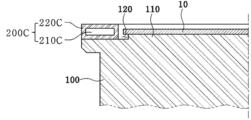
前記温度補償部材は、
前記支持部材と同じ素材からなり、前記支持部材と一体に形成される胴体部と、
前記胴体部の表面にコーティングされ、前記胴体部と異なる素材からなるコーティング層と、を含み、
前記温度補償部材の表面は洗浄ガスに対して耐食性を有する素材からなり、
前記基板は側面と縁部の下面が露出されるように前記陷沒部に配置され、前記コーティング層は前記胴体部より熱伝導率が高い材料からなり、前記コーティング層の一部は前記陷沒部の側面及び底面上に配置され、前記コーティング層の他の部分は前記基板の縁部の下面と接触するように構成され、前記コーティング層から放出される熱によって加熱されるように構成されることを特徴とする基板支持装置。 - 前記支持部材は石英からなり、前記温度補償部材は少なくとも一部が黒体からなることを特徴とする、請求項8に記載の基板支持装置。
- 前記温度補償部材の表面は、洗浄ガスに対して耐食性を有する素材でコートされることを特徴とする、請求項8に記載の基板支持装置。
- 前記黒体は、炭化ケイ素(SiC)、ブラックセラミック( Black ceramic)、酸化アルミニウム(Al2O3)、グラファイト(graphite)、及びブラック石英(Black Quartz)の少なくとも1種の物質を含むことを特徴とする、請求項9に記載の基板支持装置。
- コーティング層は、
胴体部の上面と側面の上に形成された第1コーティング層と、
前記陷沒部との下面と側面の上に形成された第2コーティング層と、
を含み、
前記第2コーティング層と前記基板の縁部は垂直方向に互いに向かい合って配置されることを特徴とする、請求項8に記載の基板支持装置。
Applications Claiming Priority (3)
| Application Number | Priority Date | Filing Date | Title |
|---|---|---|---|
| KR10-2017-0079595 | 2017-06-23 | ||
| KR20170079595 | 2017-06-23 | ||
| PCT/KR2018/007186 WO2018236201A1 (ko) | 2017-06-23 | 2018-06-25 | 기판 지지장치 |
Publications (3)
| Publication Number | Publication Date |
|---|---|
| JP2020524892A JP2020524892A (ja) | 2020-08-20 |
| JP2020524892A5 JP2020524892A5 (ja) | 2021-08-05 |
| JP7345397B2 true JP7345397B2 (ja) | 2023-09-15 |
Family
ID=64737692
Family Applications (1)
| Application Number | Title | Priority Date | Filing Date |
|---|---|---|---|
| JP2019559270A Active JP7345397B2 (ja) | 2017-06-23 | 2018-06-25 | 基板支持装置 |
Country Status (6)
| Country | Link |
|---|---|
| US (1) | US11417562B2 (ja) |
| JP (1) | JP7345397B2 (ja) |
| KR (1) | KR102147326B1 (ja) |
| CN (1) | CN110622291B (ja) |
| TW (1) | TWI793137B (ja) |
| WO (1) | WO2018236201A1 (ja) |
Families Citing this family (17)
| Publication number | Priority date | Publication date | Assignee | Title |
|---|---|---|---|---|
| US6795998B1 (en) * | 2000-07-24 | 2004-09-28 | Illinois Tool Works, Inc. | Swab with pull-truded tip |
| KR100766017B1 (ko) * | 2004-09-23 | 2007-10-10 | 유계춘 | 스티로폴 관 |
| KR100780703B1 (ko) * | 2005-04-11 | 2007-11-30 | 전남대학교산학협력단 | 연속압출식 추출장치 |
| KR100723262B1 (ko) * | 2005-06-14 | 2007-05-31 | 오현오 | 휴대용 온수공급기 |
| KR100743596B1 (ko) * | 2005-08-16 | 2007-07-27 | 주식회사 협성히스코 | 압력계 |
| KR100720002B1 (ko) * | 2006-06-09 | 2007-05-21 | 조현찬 | 금속무늬를 인쇄한 보석 및 그 제조방법 |
| KR100712227B1 (ko) * | 2006-06-15 | 2007-04-27 | 이운갑 | 정미기 및 그 정미기를 이용하여 도정된 흑미 |
| KR100764123B1 (ko) * | 2006-07-20 | 2007-10-09 | 광신금속(주) | 외줄형 가시철선 및 이를 이용한 윤형 철조망 |
| KR100746236B1 (ko) * | 2006-10-02 | 2007-08-06 | 정광용 | 자연적인 그늘막을 형성하는 나뭇가지 및 나뭇잎과 열매,꽃들로 구성된 자연 파라솔 |
| KR100741292B1 (ko) * | 2007-02-16 | 2007-07-23 | 종 완 김 | 신발끈에 의해 다양한 형태가 가능한 신발 |
| KR100727289B1 (ko) * | 2007-02-27 | 2007-06-13 | 주식회사삼영이앤티 | 슬러지 수집기의 장력조절장치 |
| KR100733029B1 (ko) * | 2007-02-27 | 2007-06-28 | 주식회사 누리플랜 | 가로등 |
| KR100746353B1 (ko) * | 2007-05-21 | 2007-08-03 | (주)맥스미디어 | 방습스피커 어셈블리 |
| KR100778779B1 (ko) * | 2007-06-22 | 2007-11-27 | 통명석재 주식회사 | 석재용 스크래치 장치 |
| DE102020110570A1 (de) * | 2020-04-17 | 2021-10-21 | Aixtron Se | CVD-Verfahren und CVD-Reaktor mit austauschbaren mit dem Substrat Wärme austauschenden Körpern |
| US20240247404A1 (en) * | 2023-01-25 | 2024-07-25 | Applied Materials, Inc. | Pre-heat rings and processing chambers including black quartz, and related methods |
| CN117594489A (zh) * | 2023-11-21 | 2024-02-23 | 深圳市华盈微技术有限公司 | 均温盘组件、半导体晶圆烘烤设备和晶圆烘烤热辐射补偿方法 |
Citations (5)
| Publication number | Priority date | Publication date | Assignee | Title |
|---|---|---|---|---|
| JP2001189375A (ja) | 1999-10-18 | 2001-07-10 | Hitachi Kokusai Electric Inc | 基板処理装置および半導体装置の製造方法 |
| JP2005142529A (ja) | 2003-10-16 | 2005-06-02 | Tokyo Electron Ltd | 成膜装置 |
| JP2010225645A (ja) | 2009-03-19 | 2010-10-07 | Dainippon Screen Mfg Co Ltd | 熱処理装置 |
| JP2012134504A (ja) | 2010-12-23 | 2012-07-12 | Samsung Led Co Ltd | 化学気相蒸着装置用サセプタ、化学気相蒸着装置及び化学気相蒸着装置を用いる基板の加熱方法 |
| JP2016530730A (ja) | 2013-09-16 | 2016-09-29 | アプライド マテリアルズ インコーポレイテッドApplied Materials,Incorporated | エピ予熱リング |
Family Cites Families (14)
| Publication number | Priority date | Publication date | Assignee | Title |
|---|---|---|---|---|
| JPH01291421A (ja) * | 1988-05-19 | 1989-11-24 | Toshiba Corp | 気相成長装置 |
| US6589352B1 (en) | 1999-12-10 | 2003-07-08 | Applied Materials, Inc. | Self aligning non contact shadow ring process kit |
| KR20030059745A (ko) * | 2002-01-04 | 2003-07-10 | 주성엔지니어링(주) | 반사기를 이용한 웨이퍼 온도 보상기 |
| DE10261362B8 (de) * | 2002-12-30 | 2008-08-28 | Osram Opto Semiconductors Gmbh | Substrat-Halter |
| US6888104B1 (en) * | 2004-02-05 | 2005-05-03 | Applied Materials, Inc. | Thermally matched support ring for substrate processing chamber |
| CN101587881A (zh) * | 2008-05-19 | 2009-11-25 | 海华科技股份有限公司 | 具有温度补偿控制石英振荡器的模块集成电路封装结构 |
| JP2011018772A (ja) * | 2009-07-09 | 2011-01-27 | Nippon Steel Corp | 炭化珪素単結晶成膜装置用サセプタ |
| KR101002748B1 (ko) * | 2009-11-17 | 2010-12-21 | (주)앤피에스 | 서셉터 유닛 및 이를 구비하는 기판 열처리 장치 |
| US8979087B2 (en) * | 2011-07-29 | 2015-03-17 | Applied Materials, Inc. | Substrate supporting edge ring with coating for improved soak performance |
| JP5965122B2 (ja) * | 2011-09-26 | 2016-08-03 | 株式会社Screenホールディングス | 熱処理方法および熱処理装置 |
| US9403251B2 (en) * | 2012-10-17 | 2016-08-02 | Applied Materials, Inc. | Minimal contact edge ring for rapid thermal processing |
| CN103074673A (zh) | 2012-12-26 | 2013-05-01 | 光达光电设备科技(嘉兴)有限公司 | 衬底支撑结构及沉积装置 |
| JP6321509B2 (ja) * | 2014-09-24 | 2018-05-09 | 東京エレクトロン株式会社 | 基板処理装置及び基板載置ユニットの製造方法 |
| JP6602145B2 (ja) * | 2015-10-13 | 2019-11-06 | 大陽日酸株式会社 | 基板載置台及び気相成長装置 |
-
2018
- 2018-06-25 JP JP2019559270A patent/JP7345397B2/ja active Active
- 2018-06-25 KR KR1020180073025A patent/KR102147326B1/ko active Active
- 2018-06-25 TW TW107121769A patent/TWI793137B/zh active
- 2018-06-25 US US16/613,115 patent/US11417562B2/en active Active
- 2018-06-25 WO PCT/KR2018/007186 patent/WO2018236201A1/ko not_active Ceased
- 2018-06-25 CN CN201880029938.2A patent/CN110622291B/zh active Active
Patent Citations (5)
| Publication number | Priority date | Publication date | Assignee | Title |
|---|---|---|---|---|
| JP2001189375A (ja) | 1999-10-18 | 2001-07-10 | Hitachi Kokusai Electric Inc | 基板処理装置および半導体装置の製造方法 |
| JP2005142529A (ja) | 2003-10-16 | 2005-06-02 | Tokyo Electron Ltd | 成膜装置 |
| JP2010225645A (ja) | 2009-03-19 | 2010-10-07 | Dainippon Screen Mfg Co Ltd | 熱処理装置 |
| JP2012134504A (ja) | 2010-12-23 | 2012-07-12 | Samsung Led Co Ltd | 化学気相蒸着装置用サセプタ、化学気相蒸着装置及び化学気相蒸着装置を用いる基板の加熱方法 |
| JP2016530730A (ja) | 2013-09-16 | 2016-09-29 | アプライド マテリアルズ インコーポレイテッドApplied Materials,Incorporated | エピ予熱リング |
Also Published As
| Publication number | Publication date |
|---|---|
| TWI793137B (zh) | 2023-02-21 |
| KR102147326B1 (ko) | 2020-08-24 |
| KR20190000850A (ko) | 2019-01-03 |
| US11417562B2 (en) | 2022-08-16 |
| TW201906069A (zh) | 2019-02-01 |
| CN110622291B (zh) | 2024-05-14 |
| WO2018236201A1 (ko) | 2018-12-27 |
| CN110622291A (zh) | 2019-12-27 |
| JP2020524892A (ja) | 2020-08-20 |
| US20210082738A1 (en) | 2021-03-18 |
Similar Documents
| Publication | Publication Date | Title |
|---|---|---|
| JP7345397B2 (ja) | 基板支持装置 | |
| JP5707766B2 (ja) | サセプタおよび半導体製造装置 | |
| TWI570258B (zh) | 具有高放射率表面的氣體散佈噴頭 | |
| JP5748699B2 (ja) | 材料層を堆積するための装置および方法 | |
| US9396909B2 (en) | Gas dispersion apparatus | |
| TWI875850B (zh) | 用於改進基板上的邊緣薄膜厚度均勻性的處理套件 | |
| US20160068996A1 (en) | Susceptor and pre-heat ring for thermal processing of substrates | |
| TWI778370B (zh) | 用於磊晶腔室的隔熱組件 | |
| WO2004090960A1 (ja) | 載置台構造及びこの載置台構造を有する熱処理装置 | |
| US9677177B2 (en) | Substrate support with quadrants | |
| KR20030097861A (ko) | 열 분산 플레이트 및 에지 지지대를 구비하는 어셈블리 | |
| KR102871352B1 (ko) | 증기 전달 방법들 및 장치 | |
| TWM545140U (zh) | 用於在cvd或pvd反應器之製程室中固持基板之裝置 | |
| KR20130073407A (ko) | 외부 가열용기를 포함하는 고온 증발원 | |
| JP5440589B2 (ja) | 気相成長装置及びエピタキシャルウェーハの製造方法 | |
| US11021790B2 (en) | Liner for processing chamber | |
| CN104934345A (zh) | 一种等离子体装置 | |
| KR100830237B1 (ko) | 대면적 기판 처리 시스템의 서셉터 구조물 | |
| KR20120038287A (ko) | 서셉터 | |
| EP4372122A2 (en) | Deposition source and deposition apparatus including the same | |
| KR20080114284A (ko) | 개선된 가열 지지부재를 구비한 화학증착장치 | |
| TW202320214A (zh) | 基板支撐件 | |
| TW202314034A (zh) | 化學氣相沉積系統及其組合 | |
| KR20020084478A (ko) | 반도체 장치의 제조를 위한 증착 장치 | |
| TW201819678A (zh) | 用於半導體製程中基板之承載及加熱之組合體及成膜裝置 |
Legal Events
| Date | Code | Title | Description |
|---|---|---|---|
| A521 | Request for written amendment filed |
Free format text: JAPANESE INTERMEDIATE CODE: A523 Effective date: 20210618 |
|
| A621 | Written request for application examination |
Free format text: JAPANESE INTERMEDIATE CODE: A621 Effective date: 20210618 |
|
| A977 | Report on retrieval |
Free format text: JAPANESE INTERMEDIATE CODE: A971007 Effective date: 20220712 |
|
| A131 | Notification of reasons for refusal |
Free format text: JAPANESE INTERMEDIATE CODE: A131 Effective date: 20220726 |
|
| A521 | Request for written amendment filed |
Free format text: JAPANESE INTERMEDIATE CODE: A523 Effective date: 20221020 |
|
| A131 | Notification of reasons for refusal |
Free format text: JAPANESE INTERMEDIATE CODE: A131 Effective date: 20230214 |
|
| A521 | Request for written amendment filed |
Free format text: JAPANESE INTERMEDIATE CODE: A523 Effective date: 20230511 |
|
| TRDD | Decision of grant or rejection written | ||
| A01 | Written decision to grant a patent or to grant a registration (utility model) |
Free format text: JAPANESE INTERMEDIATE CODE: A01 Effective date: 20230808 |
|
| A61 | First payment of annual fees (during grant procedure) |
Free format text: JAPANESE INTERMEDIATE CODE: A61 Effective date: 20230905 |
|
| R150 | Certificate of patent or registration of utility model |
Ref document number: 7345397 Country of ref document: JP Free format text: JAPANESE INTERMEDIATE CODE: R150 |