JP7200460B2 - パッケージ構造物 - Google Patents
パッケージ構造物 Download PDFInfo
- Publication number
- JP7200460B2 JP7200460B2 JP2019100507A JP2019100507A JP7200460B2 JP 7200460 B2 JP7200460 B2 JP 7200460B2 JP 2019100507 A JP2019100507 A JP 2019100507A JP 2019100507 A JP2019100507 A JP 2019100507A JP 7200460 B2 JP7200460 B2 JP 7200460B2
- Authority
- JP
- Japan
- Prior art keywords
- substrate
- package structure
- stiffener
- reinforcing member
- interposer
- Prior art date
- Legal status (The legal status is an assumption and is not a legal conclusion. Google has not performed a legal analysis and makes no representation as to the accuracy of the status listed.)
- Active
Links
Images

Classifications
-
- H—ELECTRICITY
- H01—ELECTRIC ELEMENTS
- H01L—SEMICONDUCTOR DEVICES NOT COVERED BY CLASS H10
- H01L24/00—Arrangements for connecting or disconnecting semiconductor or solid-state bodies; Methods or apparatus related thereto
- H01L24/93—Batch processes
- H01L24/95—Batch processes at chip-level, i.e. with connecting carried out on a plurality of singulated devices, i.e. on diced chips
- H01L24/97—Batch processes at chip-level, i.e. with connecting carried out on a plurality of singulated devices, i.e. on diced chips the devices being connected to a common substrate, e.g. interposer, said common substrate being separable into individual assemblies after connecting
-
- H—ELECTRICITY
- H01—ELECTRIC ELEMENTS
- H01L—SEMICONDUCTOR DEVICES NOT COVERED BY CLASS H10
- H01L23/00—Details of semiconductor or other solid state devices
- H01L23/12—Mountings, e.g. non-detachable insulating substrates
- H01L23/13—Mountings, e.g. non-detachable insulating substrates characterised by the shape
-
- H—ELECTRICITY
- H01—ELECTRIC ELEMENTS
- H01L—SEMICONDUCTOR DEVICES NOT COVERED BY CLASS H10
- H01L23/00—Details of semiconductor or other solid state devices
- H01L23/28—Encapsulations, e.g. encapsulating layers, coatings, e.g. for protection
- H01L23/29—Encapsulations, e.g. encapsulating layers, coatings, e.g. for protection characterised by the material, e.g. carbon
-
- H—ELECTRICITY
- H01—ELECTRIC ELEMENTS
- H01L—SEMICONDUCTOR DEVICES NOT COVERED BY CLASS H10
- H01L23/00—Details of semiconductor or other solid state devices
- H01L23/32—Holders for supporting the complete device in operation, i.e. detachable fixtures
Landscapes
- Engineering & Computer Science (AREA)
- Computer Hardware Design (AREA)
- Microelectronics & Electronic Packaging (AREA)
- Power Engineering (AREA)
- Physics & Mathematics (AREA)
- Condensed Matter Physics & Semiconductors (AREA)
- General Physics & Mathematics (AREA)
- Structure Of Printed Boards (AREA)
- Combinations Of Printed Boards (AREA)
Description
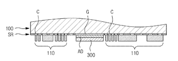
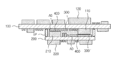
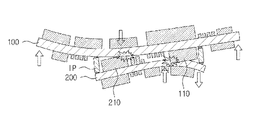
200 第2基板
IP インターポーザ
300、300' 補強材
400 充填部材
Claims (13)
- インターポーザで上下結合した第1基板及び第2基板と、
前記第1基板の前記第2基板に向かい合う一面に実装された第1素子と、
前記第1基板の前記一面に、前記第1素子から離隔して付着される補強材と、
前記補強材の向かい側に位置するように、前記第2基板の一面に実装される第2素子と、を含むパッケージ構造物。 - 前記補強材と前記第2素子との間に介在され、前記補強材及び前記第2素子のそれぞれと接触する充填部材をさらに含む請求項1に記載のパッケージ構造物。
- 前記充填部材は、熱伝導素材を含む請求項2に記載のパッケージ構造物。
- 前記インターポーザは、中空部を含み、
前記第1素子、前記補強材及び前記第2素子は、前記中空部内に収容され、
前記充填部材が前記中空部を充填する請求項2又は3に記載のパッケージ構造物。 - 前記インターポーザは、中空部を含み、
前記第1素子、前記補強材及び前記第2素子は、前記中空部内に収容される請求項1~4の何れか一項に記載のパッケージ構造物。 - 前記第1基板の最外層には、ソルダーレジストが備えられ、
前記ソルダーレジストは、前記第1基板の回路層を露出させ、
前記補強材が、露出された前記回路層に付着される請求項1~5の何れか一項に記載のパッケージ構造物。 - 前記補強材は、前記回路層よりも剛性の大きい金属を含む材質で形成される請求項6に記載のパッケージ構造物。
- 前記補強材は、ダミーダイ(dummy die)を含む請求項1~7の何れか一項に記載のパッケージ構造物。
- 前記ダミーダイの厚さは、前記第1素子の厚さよりも小さい請求項8に記載のパッケージ構造物。
- 前記第1素子は、複数で構成され、
前記補強材は、前記複数の第1素子の間に配置される請求項1~9の何れか一項に記載のパッケージ構造物。 - 前記補強材は、接着剤またはソルダーで付着される請求項1~10の何れか一項に記載のパッケージ構造物。
- 前記第2基板の前記一面に、前記第2素子から離隔して付着される第2の補強材をさらに含む請求項1~11の何れか一項に記載のパッケージ構造物。
- 前記第1素子と前記第2の補強材とは互いに向かい側に位置し、
前記第1素子と前記第2の補強材との間に介在され、前記第1素子及び前記第2の補強材のそれぞれと接触する充填部材をさらに含む請求項12に記載のパッケージ構造物。
Applications Claiming Priority (2)
| Application Number | Priority Date | Filing Date | Title |
|---|---|---|---|
| KR10-2018-0139325 | 2018-11-13 | ||
| KR1020180139325A KR102561946B1 (ko) | 2018-11-13 | 2018-11-13 | 패키지 구조물 |
Publications (2)
| Publication Number | Publication Date |
|---|---|
| JP2020080398A JP2020080398A (ja) | 2020-05-28 |
| JP7200460B2 true JP7200460B2 (ja) | 2023-01-10 |
Family
ID=70802507
Family Applications (1)
| Application Number | Title | Priority Date | Filing Date |
|---|---|---|---|
| JP2019100507A Active JP7200460B2 (ja) | 2018-11-13 | 2019-05-29 | パッケージ構造物 |
Country Status (3)
| Country | Link |
|---|---|
| JP (1) | JP7200460B2 (ja) |
| KR (1) | KR102561946B1 (ja) |
| TW (1) | TWI793319B (ja) |
Families Citing this family (1)
| Publication number | Priority date | Publication date | Assignee | Title |
|---|---|---|---|---|
| WO2025146949A1 (ko) * | 2024-01-02 | 2025-07-10 | 삼성전자주식회사 | 열 전달 물질을 포함하는 인쇄 회로 기판을 포함하는 전자 장치 |
Citations (8)
| Publication number | Priority date | Publication date | Assignee | Title |
|---|---|---|---|---|
| US20040089943A1 (en) | 2002-11-07 | 2004-05-13 | Masato Kirigaya | Electronic control device and method for manufacturing the same |
| JP2006173152A (ja) | 2004-12-13 | 2006-06-29 | Matsushita Electric Ind Co Ltd | 中継基板と立体配線構造体 |
| JP2006210852A (ja) | 2005-01-31 | 2006-08-10 | Toshiba Corp | 表面実装型回路部品を実装する回路基板及びその製造方法 |
| JP2006261387A (ja) | 2005-03-17 | 2006-09-28 | Matsushita Electric Ind Co Ltd | モジュールとその製造方法 |
| JP2009176931A (ja) | 2008-01-24 | 2009-08-06 | Panasonic Corp | 半導体装置および電子機器 |
| JP2013026346A (ja) | 2011-07-19 | 2013-02-04 | Toshiba Corp | 半導体装置 |
| JP2014165481A (ja) | 2013-02-28 | 2014-09-08 | Kyocer Slc Technologies Corp | 半導体素子実装体 |
| US20180190622A1 (en) | 2014-03-07 | 2018-07-05 | Bridge Semiconductor Corporation | 3-d stacking semiconductor assembly having heat dissipation characteristics |
Family Cites Families (9)
| Publication number | Priority date | Publication date | Assignee | Title |
|---|---|---|---|---|
| JP2004158700A (ja) * | 2002-11-07 | 2004-06-03 | Denso Corp | 電子制御装置およびその製造方法 |
| TWI460844B (zh) * | 2009-04-06 | 2014-11-11 | 金龍國際公司 | 具有內嵌式晶片及矽導通孔晶粒之堆疊封裝結構及其製造方法 |
| US8247900B2 (en) * | 2009-12-29 | 2012-08-21 | Taiwan Semiconductor Manufacturing Company, Ltd. | Flip chip package having enhanced thermal and mechanical performance |
| TW201314935A (zh) * | 2011-09-23 | 2013-04-01 | Mke Technology Co Ltd | 太陽能電池封裝結構 |
| KR20150009728A (ko) * | 2013-07-17 | 2015-01-27 | 삼성전기주식회사 | 전자 소자 모듈 및 그 실장 구조 |
| KR101324595B1 (ko) | 2013-08-07 | 2013-11-01 | (주)드림텍 | 조립성 및 유동성이 우수한 휴대 단말기용 메인 보드 |
| JP2016025143A (ja) * | 2014-07-17 | 2016-02-08 | イビデン株式会社 | 回路基板及びその製造方法 |
| JP2016173152A (ja) * | 2015-03-17 | 2016-09-29 | Ntn株式会社 | 保持器および転がり軸受 |
| WO2018125242A1 (en) * | 2016-12-30 | 2018-07-05 | Intel Corporation | Microelectronic devices designed with 3d stacked ultra thin package modules for high frequency communications |
-
2018
- 2018-11-13 KR KR1020180139325A patent/KR102561946B1/ko active Active
-
2019
- 2019-05-08 TW TW108115817A patent/TWI793319B/zh active
- 2019-05-29 JP JP2019100507A patent/JP7200460B2/ja active Active
Patent Citations (8)
| Publication number | Priority date | Publication date | Assignee | Title |
|---|---|---|---|---|
| US20040089943A1 (en) | 2002-11-07 | 2004-05-13 | Masato Kirigaya | Electronic control device and method for manufacturing the same |
| JP2006173152A (ja) | 2004-12-13 | 2006-06-29 | Matsushita Electric Ind Co Ltd | 中継基板と立体配線構造体 |
| JP2006210852A (ja) | 2005-01-31 | 2006-08-10 | Toshiba Corp | 表面実装型回路部品を実装する回路基板及びその製造方法 |
| JP2006261387A (ja) | 2005-03-17 | 2006-09-28 | Matsushita Electric Ind Co Ltd | モジュールとその製造方法 |
| JP2009176931A (ja) | 2008-01-24 | 2009-08-06 | Panasonic Corp | 半導体装置および電子機器 |
| JP2013026346A (ja) | 2011-07-19 | 2013-02-04 | Toshiba Corp | 半導体装置 |
| JP2014165481A (ja) | 2013-02-28 | 2014-09-08 | Kyocer Slc Technologies Corp | 半導体素子実装体 |
| US20180190622A1 (en) | 2014-03-07 | 2018-07-05 | Bridge Semiconductor Corporation | 3-d stacking semiconductor assembly having heat dissipation characteristics |
Also Published As
| Publication number | Publication date |
|---|---|
| KR102561946B1 (ko) | 2023-08-01 |
| KR20200055555A (ko) | 2020-05-21 |
| TWI793319B (zh) | 2023-02-21 |
| TW202018881A (zh) | 2020-05-16 |
| JP2020080398A (ja) | 2020-05-28 |
Similar Documents
| Publication | Publication Date | Title |
|---|---|---|
| US7242092B2 (en) | Substrate assembly with direct electrical connection as a semiconductor package | |
| US6525942B2 (en) | Heat dissipation ball grid array package | |
| CN101159254B (zh) | 半导体装置 | |
| KR101476385B1 (ko) | 접착성 스페이싱 구조들을 갖는 마운트가능한 집적회로패키지-인-패키지 시스템 | |
| JP3110922B2 (ja) | マルチチップ・モジュール | |
| US8553420B2 (en) | Enhanced stacked microelectronic assemblies with central contacts and improved thermal characteristics | |
| US8263871B2 (en) | Mount board and semiconductor module | |
| JP5413971B2 (ja) | 電子部品実装装置及びその製造方法 | |
| US8304922B2 (en) | Semiconductor package system with thermal die bonding | |
| TWI778236B (zh) | 半導體裝置 | |
| KR100698526B1 (ko) | 방열층을 갖는 배선기판 및 그를 이용한 반도체 패키지 | |
| KR20140057982A (ko) | 반도체 패키지 및 반도체 패키지의 제조 방법 | |
| US8970044B2 (en) | Integrated circuit packaging system with vertical interconnects and method of manufacture thereof | |
| KR100768998B1 (ko) | 다층인쇄회로기판을 사용한 범프접속형 칩실장모듈 | |
| JP7200460B2 (ja) | パッケージ構造物 | |
| TWI391084B (zh) | 具有散熱件之電路板結構 | |
| JP4627323B2 (ja) | 半導体装置 | |
| JP4919689B2 (ja) | モジュール基板 | |
| JP3024596B2 (ja) | フィルムキャリアテープを用いたbga型半導体装置 | |
| KR20210035027A (ko) | 전자 소자 모듈 및 그 제조 방법 | |
| CN120432448B (zh) | 一种ic封装结构及封装方法 | |
| US20250379113A1 (en) | Semiconductor package and manufacturing method thereof | |
| JP3965867B2 (ja) | 半導体パッケージ | |
| CN100505227C (zh) | 半导体封装直接电性连接的基板结构 | |
| JP2904754B2 (ja) | 電子部品の実装用配線基板 |
Legal Events
| Date | Code | Title | Description |
|---|---|---|---|
| A621 | Written request for application examination |
Free format text: JAPANESE INTERMEDIATE CODE: A621 Effective date: 20211104 |
|
| A977 | Report on retrieval |
Free format text: JAPANESE INTERMEDIATE CODE: A971007 Effective date: 20221110 |
|
| TRDD | Decision of grant or rejection written | ||
| A01 | Written decision to grant a patent or to grant a registration (utility model) |
Free format text: JAPANESE INTERMEDIATE CODE: A01 Effective date: 20221122 |
|
| A61 | First payment of annual fees (during grant procedure) |
Free format text: JAPANESE INTERMEDIATE CODE: A61 Effective date: 20221130 |
|
| R150 | Certificate of patent or registration of utility model |
Ref document number: 7200460 Country of ref document: JP Free format text: JAPANESE INTERMEDIATE CODE: R150 |
|
| R250 | Receipt of annual fees |
Free format text: JAPANESE INTERMEDIATE CODE: R250 |