JP7061810B2 - 低損失電送機構及びそれを使用するアンテナ - Google Patents
低損失電送機構及びそれを使用するアンテナ Download PDFInfo
- Publication number
- JP7061810B2 JP7061810B2 JP2019531126A JP2019531126A JP7061810B2 JP 7061810 B2 JP7061810 B2 JP 7061810B2 JP 2019531126 A JP2019531126 A JP 2019531126A JP 2019531126 A JP2019531126 A JP 2019531126A JP 7061810 B2 JP7061810 B2 JP 7061810B2
- Authority
- JP
- Japan
- Prior art keywords
- substrate
- conductive circuit
- insulating plate
- conductive
- dielectric
- Prior art date
- Legal status (The legal status is an assumption and is not a legal conclusion. Google has not performed a legal analysis and makes no representation as to the accuracy of the status listed.)
- Active
Links
- 230000005540 biological transmission Effects 0.000 title claims description 27
- 230000007246 mechanism Effects 0.000 title description 3
- 239000000758 substrate Substances 0.000 claims description 67
- 239000000463 material Substances 0.000 claims description 25
- 238000000034 method Methods 0.000 claims description 19
- -1 polytetrafluoroethylene Polymers 0.000 claims description 18
- 230000006835 compression Effects 0.000 claims description 14
- 238000007906 compression Methods 0.000 claims description 14
- 239000003989 dielectric material Substances 0.000 claims description 14
- 229920001343 polytetrafluoroethylene Polymers 0.000 claims description 9
- 239000004810 polytetrafluoroethylene Substances 0.000 claims description 9
- 210000004907 gland Anatomy 0.000 claims description 8
- 239000012212 insulator Substances 0.000 claims description 8
- 239000005020 polyethylene terephthalate Substances 0.000 claims description 8
- 229920000139 polyethylene terephthalate Polymers 0.000 claims description 8
- 239000004642 Polyimide Substances 0.000 claims description 7
- 229920001721 polyimide Polymers 0.000 claims description 7
- 239000004743 Polypropylene Substances 0.000 claims description 6
- 229920001155 polypropylene Polymers 0.000 claims description 6
- 239000000853 adhesive Substances 0.000 claims description 5
- 230000001070 adhesive effect Effects 0.000 claims description 5
- 238000004519 manufacturing process Methods 0.000 claims description 4
- 238000007772 electroless plating Methods 0.000 claims description 3
- 239000003365 glass fiber Substances 0.000 claims description 3
- 238000009413 insulation Methods 0.000 claims description 3
- 238000003825 pressing Methods 0.000 claims description 3
- 239000000126 substance Substances 0.000 claims 1
- 239000010408 film Substances 0.000 description 24
- 229920006362 Teflon® Polymers 0.000 description 13
- RYGMFSIKBFXOCR-UHFFFAOYSA-N Copper Chemical compound [Cu] RYGMFSIKBFXOCR-UHFFFAOYSA-N 0.000 description 11
- 239000004020 conductor Substances 0.000 description 11
- 239000011230 binding agent Substances 0.000 description 9
- 229910052802 copper Inorganic materials 0.000 description 9
- 239000010949 copper Substances 0.000 description 9
- 230000005855 radiation Effects 0.000 description 9
- 239000004809 Teflon Substances 0.000 description 8
- 239000011521 glass Substances 0.000 description 7
- 125000006850 spacer group Chemical group 0.000 description 7
- XEEYBQQBJWHFJM-UHFFFAOYSA-N Iron Chemical compound [Fe] XEEYBQQBJWHFJM-UHFFFAOYSA-N 0.000 description 6
- 230000008901 benefit Effects 0.000 description 6
- 239000010409 thin film Substances 0.000 description 6
- 238000000926 separation method Methods 0.000 description 5
- 239000011248 coating agent Substances 0.000 description 3
- 238000000576 coating method Methods 0.000 description 3
- 238000010438 heat treatment Methods 0.000 description 3
- 229910052742 iron Inorganic materials 0.000 description 3
- 239000002184 metal Substances 0.000 description 3
- 229910052751 metal Inorganic materials 0.000 description 3
- 230000008569 process Effects 0.000 description 3
- 238000004544 sputter deposition Methods 0.000 description 3
- 239000004988 Nematic liquid crystal Substances 0.000 description 2
- 230000015572 biosynthetic process Effects 0.000 description 2
- 238000013461 design Methods 0.000 description 2
- 238000009713 electroplating Methods 0.000 description 2
- 238000005516 engineering process Methods 0.000 description 2
- 238000005755 formation reaction Methods 0.000 description 2
- 239000003292 glue Substances 0.000 description 2
- 238000007747 plating Methods 0.000 description 2
- 238000007639 printing Methods 0.000 description 2
- 239000004593 Epoxy Substances 0.000 description 1
- 238000013459 approach Methods 0.000 description 1
- 239000011324 bead Substances 0.000 description 1
- 239000000969 carrier Substances 0.000 description 1
- 239000012876 carrier material Substances 0.000 description 1
- 238000004891 communication Methods 0.000 description 1
- 230000008602 contraction Effects 0.000 description 1
- 230000000694 effects Effects 0.000 description 1
- 238000007429 general method Methods 0.000 description 1
- 239000011810 insulating material Substances 0.000 description 1
- 239000004973 liquid crystal related substance Substances 0.000 description 1
- 239000000203 mixture Substances 0.000 description 1
- 238000012986 modification Methods 0.000 description 1
- 230000004048 modification Effects 0.000 description 1
- 230000010363 phase shift Effects 0.000 description 1
- 230000010287 polarization Effects 0.000 description 1
- 230000008054 signal transmission Effects 0.000 description 1
- 229910000679 solder Inorganic materials 0.000 description 1
Images


Classifications
-
- H—ELECTRICITY
- H01—ELECTRIC ELEMENTS
- H01Q—ANTENNAS, i.e. RADIO AERIALS
- H01Q13/00—Waveguide horns or mouths; Slot antennas; Leaky-waveguide antennas; Equivalent structures causing radiation along the transmission path of a guided wave
- H01Q13/20—Non-resonant leaky-waveguide or transmission-line antennas; Equivalent structures causing radiation along the transmission path of a guided wave
- H01Q13/206—Microstrip transmission line antennas
-
- H—ELECTRICITY
- H01—ELECTRIC ELEMENTS
- H01Q—ANTENNAS, i.e. RADIO AERIALS
- H01Q9/00—Electrically-short antennas having dimensions not more than twice the operating wavelength and consisting of conductive active radiating elements
- H01Q9/04—Resonant antennas
- H01Q9/0407—Substantially flat resonant element parallel to ground plane, e.g. patch antenna
- H01Q9/045—Substantially flat resonant element parallel to ground plane, e.g. patch antenna with particular feeding means
- H01Q9/0457—Substantially flat resonant element parallel to ground plane, e.g. patch antenna with particular feeding means electromagnetically coupled to the feed line
-
- H—ELECTRICITY
- H01—ELECTRIC ELEMENTS
- H01P—WAVEGUIDES; RESONATORS, LINES, OR OTHER DEVICES OF THE WAVEGUIDE TYPE
- H01P1/00—Auxiliary devices
- H01P1/18—Phase-shifters
- H01P1/181—Phase-shifters using ferroelectric devices
-
- H—ELECTRICITY
- H01—ELECTRIC ELEMENTS
- H01P—WAVEGUIDES; RESONATORS, LINES, OR OTHER DEVICES OF THE WAVEGUIDE TYPE
- H01P3/00—Waveguides; Transmission lines of the waveguide type
- H01P3/02—Waveguides; Transmission lines of the waveguide type with two longitudinal conductors
- H01P3/08—Microstrips; Strip lines
- H01P3/081—Microstriplines
- H01P3/082—Multilayer dielectric
-
- H—ELECTRICITY
- H01—ELECTRIC ELEMENTS
- H01P—WAVEGUIDES; RESONATORS, LINES, OR OTHER DEVICES OF THE WAVEGUIDE TYPE
- H01P3/00—Waveguides; Transmission lines of the waveguide type
- H01P3/02—Waveguides; Transmission lines of the waveguide type with two longitudinal conductors
- H01P3/08—Microstrips; Strip lines
- H01P3/081—Microstriplines
- H01P3/084—Suspended microstriplines
-
- H—ELECTRICITY
- H01—ELECTRIC ELEMENTS
- H01P—WAVEGUIDES; RESONATORS, LINES, OR OTHER DEVICES OF THE WAVEGUIDE TYPE
- H01P3/00—Waveguides; Transmission lines of the waveguide type
- H01P3/02—Waveguides; Transmission lines of the waveguide type with two longitudinal conductors
- H01P3/08—Microstrips; Strip lines
- H01P3/088—Stacked transmission lines
-
- H—ELECTRICITY
- H01—ELECTRIC ELEMENTS
- H01Q—ANTENNAS, i.e. RADIO AERIALS
- H01Q1/00—Details of, or arrangements associated with, antennas
- H01Q1/36—Structural form of radiating elements, e.g. cone, spiral, umbrella; Particular materials used therewith
- H01Q1/38—Structural form of radiating elements, e.g. cone, spiral, umbrella; Particular materials used therewith formed by a conductive layer on an insulating support
-
- H—ELECTRICITY
- H01—ELECTRIC ELEMENTS
- H01Q—ANTENNAS, i.e. RADIO AERIALS
- H01Q21/00—Antenna arrays or systems
- H01Q21/06—Arrays of individually energised antenna units similarly polarised and spaced apart
- H01Q21/061—Two dimensional planar arrays
- H01Q21/065—Patch antenna array
-
- H—ELECTRICITY
- H01—ELECTRIC ELEMENTS
- H01Q—ANTENNAS, i.e. RADIO AERIALS
- H01Q3/00—Arrangements for changing or varying the orientation or the shape of the directional pattern of the waves radiated from an antenna or antenna system
- H01Q3/44—Arrangements for changing or varying the orientation or the shape of the directional pattern of the waves radiated from an antenna or antenna system varying the electric or magnetic characteristics of reflecting, refracting, or diffracting devices associated with the radiating element
-
- H—ELECTRICITY
- H01—ELECTRIC ELEMENTS
- H01Q—ANTENNAS, i.e. RADIO AERIALS
- H01Q9/00—Electrically-short antennas having dimensions not more than twice the operating wavelength and consisting of conductive active radiating elements
- H01Q9/04—Resonant antennas
- H01Q9/0407—Substantially flat resonant element parallel to ground plane, e.g. patch antenna
- H01Q9/0428—Substantially flat resonant element parallel to ground plane, e.g. patch antenna radiating a circular polarised wave
- H01Q9/0435—Substantially flat resonant element parallel to ground plane, e.g. patch antenna radiating a circular polarised wave using two feed points
-
- H—ELECTRICITY
- H04—ELECTRIC COMMUNICATION TECHNIQUE
- H04B—TRANSMISSION
- H04B1/00—Details of transmission systems, not covered by a single one of groups H04B3/00 - H04B13/00; Details of transmission systems not characterised by the medium used for transmission
- H04B1/38—Transceivers, i.e. devices in which transmitter and receiver form a structural unit and in which at least one part is used for functions of transmitting and receiving
- H04B1/40—Circuits
- H04B1/50—Circuits using different frequencies for the two directions of communication
- H04B1/52—Hybrid arrangements, i.e. arrangements for transition from single-path two-direction transmission to single-direction transmission on each of two paths or vice versa
-
- H—ELECTRICITY
- H04—ELECTRIC COMMUNICATION TECHNIQUE
- H04B—TRANSMISSION
- H04B1/00—Details of transmission systems, not covered by a single one of groups H04B3/00 - H04B13/00; Details of transmission systems not characterised by the medium used for transmission
- H04B1/38—Transceivers, i.e. devices in which transmitter and receiver form a structural unit and in which at least one part is used for functions of transmitting and receiving
- H04B1/40—Circuits
- H04B1/54—Circuits using the same frequency for two directions of communication
- H04B1/58—Hybrid arrangements, i.e. arrangements for transition from single-path two-direction transmission to single-direction transmission on each of two paths or vice versa
- H04B1/586—Hybrid arrangements, i.e. arrangements for transition from single-path two-direction transmission to single-direction transmission on each of two paths or vice versa using an electronic circuit
-
- H—ELECTRICITY
- H04—ELECTRIC COMMUNICATION TECHNIQUE
- H04B—TRANSMISSION
- H04B3/00—Line transmission systems
- H04B3/54—Systems for transmission via power distribution lines
- H04B3/56—Circuits for coupling, blocking, or by-passing of signals
Landscapes
- Engineering & Computer Science (AREA)
- Computer Networks & Wireless Communication (AREA)
- Signal Processing (AREA)
- Power Engineering (AREA)
- Physics & Mathematics (AREA)
- Electromagnetism (AREA)
- Details Of Aerials (AREA)
- Waveguide Aerials (AREA)
- Waveguides (AREA)
Description
本願は、2017年6月22日に出願の米国仮特許出願第62/523,498号、2016年12月7日に出願の米国仮特許出願第62/431,393号、2017年1月31日に出願の米国特許出願第15/421,388号、及び2017年7月19日に出願の米国特許出願第15/654,643号の優先権を主張するものであり、それらのすべての開示全体が言及によって本明細書に援用される。
本開示は、一般にアンテナの分野に関する。より具体的には、本開示は、特にアンテナに適する、電磁エネルギーを伝導する伝送機構に関する。
所定の場所同士の間で電磁エネルギーを伝導する一般的な方法は、マイクロストリッププリント技術を備えた回路板を使用すること又は金属導波路を用いることである。導波路に対する回路板の利点は、回路板がより大量に生産可能であるとともに平坦であることである。不利点は、高周波電子信号が進行する距離に比例する損失である。金属導波路の利点は小さい損失で動作することだが、不利点は、回路板ほど薄くなく、コスト効率もよくないことである。
Claims (22)
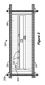
- フィルム基板と、
前記フィルム基板の一方の表面に配置された導電回路と、
前記フィルム基板に接する第1表面を有する誘電体プレートと、
前記誘電体プレートの第2表面に接する導電グランドとの組立体と、
圧縮絶縁体とを含み、
前記組立体は前記圧縮絶縁体内に配置される、電磁伝送ラインシステム。 - 前記導電回路は、前記フィルム基板と前記誘電体プレートとの間に挟まれる、請求項1に記載のシステム。
- 前記導電回路は前記フィルム基板に取り付けられ、前記誘電体プレートには取り付けられない、請求項1に記載のシステム。
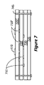
- 前記フィルム基板を覆うように配置された上部保持部材、前記導電グランドを覆うように配置された下部保持部材、及び前記上部保持部材と前記下部保持部材とに圧縮力を加える圧力アプリケータをさらに含む、請求項1に記載のシステム。
- 前記第1表面は、前記導電回路を有する前記一方の表面とは反対側で前記フィルム基板に当接する、請求項1に記載のシステム。
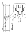
- 前記フィルム基板と前記誘電体プレートとの横方向アライメントを保持するように構成されたアライナーをさらに含む、請求項1に記載のシステム。
- 前記アライナーは誘電体ピンを含む、請求項6に記載のシステム。
- 前記フィルム基板はポリイミドを含む、請求項1に記載のシステム。
- 前記誘電体プレートは、ポリテトラフルオロエチレン、ポリエチレンテレフタレート、ポリプロピレン含浸ガラス繊維、又はポリプロピレン材料の1つを含む、請求項1に記載のシステム。
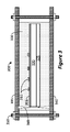
- 低誘電材料を含む絶縁プレート、前記絶縁プレートに当接する基板、前記絶縁プレートの第1表面に近接する第1導電回路、前記絶縁プレートの第2表面に近接する第2導電回路を含み、前記第1導電回路及び前記第2導電回路の少なくとも1つは、前記絶縁プレートに化学的又は機械的に接着せず、熱膨張時に前記絶縁プレートと前記第1導電回路及び前記第2導電回路の少なくとも1つとの間の滑りを可能にしつつ前記絶縁プレートに対して機械的に押圧され、
前記基板と前記絶縁プレートとの間に圧縮力を加えるよう構成された圧縮絶縁体をさらに含む、高性能電磁伝送システム。 - 前記第1導電回路及び前記第2導電回路の少なくとも1つは、前記基板に機械的又は化学的に取り付けられる、請求項10に記載のシステム。
- 前記基板と前記絶縁プレートとの間で圧縮力を加えるように構成された圧縮手段をさらに含む、請求項11に記載のシステム。
- 前記圧縮手段は、前記基板を覆うように配置された上部保持部材、前記絶縁プレートを覆うように配置された下部保持部材、及び前記上部保持部材と前記下部保持部材とに圧縮力を加える圧力アプリケータを含む、請求項12に記載のシステム。
- 前記基板は前記絶縁プレートに機械的又は化学的な手段によって物理的に取り付けられる、請求項11に記載のシステム。
- 前記第1導電回路及び前記第2導電回路の1つは、接着剤によって前記基板に固定される、請求項11に記載のシステム。
- 前記第1導電回路及び前記第2導電回路の1つは、無電解めっきによって前記基板に固定される、請求項11に記載のシステム。
- 前記基板はポリイミドを含む、請求項11に記載のシステム。
- 前記絶縁プレートは、ポリテトラフルオロエチレン、ポリエチレンテレフタレート、又はFR-4プリント回路基板の1つを含む、請求項10に記載のシステム。
- 高性能電磁伝送ラインシステムを製造する方法であって、
基板を取得するステップと、
前記基板の第1表面に第1導電回路部品を配置するステップと、
絶縁プレートを取得するステップと、
前記絶縁プレートの第1表面に第2導電回路部品を配置するステップと、
熱膨張時に前記絶縁プレートと前記第1導電回路部品と前記第2導電回路部品との少なくとも1つとの間の滑りを可能にしつつ前記基板を前記絶縁プレートに取り付けるステップと、
前記基板と前記絶縁プレートとの間に圧縮力を加えるよう構成された圧縮絶縁体を取り付けるステップとを含む、方法。 - 前記基板を前記絶縁プレートに取り付けることは、前記基板の前記第1表面を、前記絶縁プレートの第2表面に取り付けることを含む、請求項19に記載の方法。
- 前記第1導電回路部品と前記第2導電回路部品との少なくとも1つを前記絶縁プレートに接して保持するように圧力を加えることをさらに含む、請求項19に記載の方法。
- 前記絶縁プレートに誘電体ピンを挿入することをさらに含む、請求項19に記載の方法。
Applications Claiming Priority (9)
| Application Number | Priority Date | Filing Date | Title |
|---|---|---|---|
| US201662431393P | 2016-12-07 | 2016-12-07 | |
| US62/431,393 | 2016-12-07 | ||
| US15/421,388 | 2017-01-31 | ||
| US15/421,388 US10199710B2 (en) | 2016-09-01 | 2017-01-31 | Variable dielectric constant-based devices |
| US201762523498P | 2017-06-22 | 2017-06-22 | |
| US62/523,498 | 2017-06-22 | ||
| US15/654,643 | 2017-07-19 | ||
| US15/654,643 US10326205B2 (en) | 2016-09-01 | 2017-07-19 | Multi-layered software defined antenna and method of manufacture |
| PCT/US2017/063539 WO2018106485A1 (en) | 2016-12-07 | 2017-11-28 | Low loss electrical transmission mechanism and antenna using same |
Publications (2)
| Publication Number | Publication Date |
|---|---|
| JP2020501460A JP2020501460A (ja) | 2020-01-16 |
| JP7061810B2 true JP7061810B2 (ja) | 2022-05-02 |
Family
ID=62244208
Family Applications (1)
| Application Number | Title | Priority Date | Filing Date |
|---|---|---|---|
| JP2019531126A Active JP7061810B2 (ja) | 2016-12-07 | 2017-11-28 | 低損失電送機構及びそれを使用するアンテナ |
Country Status (7)
| Country | Link |
|---|---|
| US (1) | US20180159239A1 (ja) |
| EP (1) | EP3552217A4 (ja) |
| JP (1) | JP7061810B2 (ja) |
| KR (1) | KR102364013B1 (ja) |
| CN (1) | CN110140184A (ja) |
| IL (1) | IL266906B2 (ja) |
| WO (1) | WO2018106485A1 (ja) |
Families Citing this family (5)
| Publication number | Priority date | Publication date | Assignee | Title |
|---|---|---|---|---|
| WO2019079774A1 (en) * | 2017-10-19 | 2019-04-25 | Wafer, Llc | DISPERSED STATE ALIGNMENT PHASE MODULATOR DEVICE / POLYMER SHEAR |
| US10903568B2 (en) * | 2018-11-20 | 2021-01-26 | Nokia Technologies Oy | Electrochromic reflectarray antenna |
| CN110034358B (zh) * | 2019-04-04 | 2024-02-23 | 信利半导体有限公司 | 一种液晶移相器、液晶天线及液晶移相器的制作方法 |
| US11728577B2 (en) * | 2019-11-15 | 2023-08-15 | Wafer Llc | Multi-layered antenna having dual-band patch |
| CN113725597B (zh) * | 2021-09-01 | 2024-04-12 | 成都天马微电子有限公司 | 液晶天线的制作方法、液晶天线 |
Citations (1)
| Publication number | Priority date | Publication date | Assignee | Title |
|---|---|---|---|---|
| US20080238793A1 (en) | 2007-03-28 | 2008-10-02 | M/A-Com, Inc. | Compact Planar Antenna For Single and Multiple Polarization Configurations |
Family Cites Families (83)
| Publication number | Priority date | Publication date | Assignee | Title |
|---|---|---|---|---|
| US3258724A (en) * | 1966-06-28 | Strip line structures | ||
| GB1249355A (en) | 1967-12-27 | 1971-10-13 | Hitachi Ltd | Transparent sintered alumina and process for preparing the same |
| BE792698A (fr) * | 1971-12-21 | 1973-06-13 | Illinois Tool Works | Catheter-canule samenstel |
| US4105960A (en) * | 1976-12-20 | 1978-08-08 | Helmut Bacher | Broad-band continuously variable attenuator |
| US4496903A (en) * | 1981-05-11 | 1985-01-29 | Burroughs Corporation | Circuit board test fixture |
| US4657322A (en) * | 1985-10-01 | 1987-04-14 | Tektronix, Inc. | Microwave interconnect |
| US4816836A (en) * | 1986-01-29 | 1989-03-28 | Ball Corporation | Conformal antenna and method |
| US4873501A (en) * | 1986-06-27 | 1989-10-10 | The United States Of America As Represented By The Secretary Of The Navy | Internal transmission line filter element |
| US5228189A (en) * | 1988-11-12 | 1993-07-20 | Mania Gmbh & Co. | Adapter arrangement for electrically connecting flat wire carriers |
| US5155493A (en) * | 1990-08-28 | 1992-10-13 | The United States Of America As Represented By The Secretary Of The Air Force | Tape type microstrip patch antenna |
| US5406120A (en) * | 1992-10-20 | 1995-04-11 | Jones; Robert M. | Hermetically sealed semiconductor ceramic package |
| US5736783A (en) * | 1993-10-08 | 1998-04-07 | Stratedge Corporation. | High frequency microelectronics package |
| US6172412B1 (en) * | 1993-10-08 | 2001-01-09 | Stratedge Corporation | High frequency microelectronics package |
| US5753972A (en) * | 1993-10-08 | 1998-05-19 | Stratedge Corporation | Microelectronics package |
| US6271579B1 (en) * | 1993-10-08 | 2001-08-07 | Stratedge Corporation | High-frequency passband microelectronics package |
| US5465008A (en) * | 1993-10-08 | 1995-11-07 | Stratedge Corporation | Ceramic microelectronics package |
| JP3356866B2 (ja) * | 1994-04-04 | 2002-12-16 | 日立化成工業株式会社 | トリプレート給電型平面アンテナの製造法 |
| US5672226A (en) * | 1995-10-11 | 1997-09-30 | Delco Electronics Corporation | Process of forming multilayer circuit boards |
| US5726666A (en) * | 1996-04-02 | 1998-03-10 | Ems Technologies, Inc. | Omnidirectional antenna with single feedpoint |
| JPH09307342A (ja) * | 1996-05-14 | 1997-11-28 | Mitsubishi Electric Corp | アンテナ装置 |
| US5753968A (en) | 1996-08-05 | 1998-05-19 | Itt Industries, Inc. | Low loss ridged microstrip line for monolithic microwave integrated circuit (MMIC) applications |
| US6201439B1 (en) * | 1997-09-17 | 2001-03-13 | Matsushita Electric Industrial Co., Ltd. | Power splitter/ combiner circuit, high power amplifier and balun circuit |
| US6037903A (en) * | 1998-08-05 | 2000-03-14 | California Amplifier, Inc. | Slot-coupled array antenna structures |
| US6472950B1 (en) * | 1998-10-28 | 2002-10-29 | Apti, Inc. | Broadband coupled-line power combiner/divider |
| WO2001033660A1 (en) * | 1999-11-04 | 2001-05-10 | Paratek Microwave, Inc. | Microstrip tunable filters tuned by dielectric varactors |
| JP2001345212A (ja) * | 2000-05-31 | 2001-12-14 | Tdk Corp | 積層電子部品 |
| TW515890B (en) * | 2000-09-25 | 2003-01-01 | Jsr Corp | Anisotropically conductive sheet, production process thereof and applied product thereof |
| US7462852B2 (en) * | 2001-12-17 | 2008-12-09 | Tecomet, Inc. | Devices, methods, and systems involving cast collimators |
| US7785098B1 (en) * | 2001-06-05 | 2010-08-31 | Mikro Systems, Inc. | Systems for large area micro mechanical systems |
| US7518136B2 (en) * | 2001-12-17 | 2009-04-14 | Tecomet, Inc. | Devices, methods, and systems involving cast computed tomography collimators |
| CA2448736C (en) * | 2001-06-05 | 2010-08-10 | Mikro Systems, Inc. | Methods for manufacturing three-dimensional devices and devices created thereby |
| US7141812B2 (en) * | 2002-06-05 | 2006-11-28 | Mikro Systems, Inc. | Devices, methods, and systems involving castings |
| KR100588029B1 (ko) * | 2002-03-07 | 2006-06-12 | 제이에스알 가부시끼가이샤 | 이방 도전성 커넥터 및 그 제조 방법 및 회로 장치의 검사장치 |
| US6731246B2 (en) * | 2002-06-27 | 2004-05-04 | Harris Corporation | Efficient loop antenna of reduced diameter |
| US6597318B1 (en) * | 2002-06-27 | 2003-07-22 | Harris Corporation | Loop antenna and feed coupler for reduced interaction with tuning adjustments |
| US6720926B2 (en) * | 2002-06-27 | 2004-04-13 | Harris Corporation | System for improved matching and broadband performance of microwave antennas |
| US6753814B2 (en) * | 2002-06-27 | 2004-06-22 | Harris Corporation | Dipole arrangements using dielectric substrates of meta-materials |
| US6842140B2 (en) * | 2002-12-03 | 2005-01-11 | Harris Corporation | High efficiency slot fed microstrip patch antenna |
| ATE515078T1 (de) * | 2003-01-17 | 2011-07-15 | Jsr Corp | Anisotroper leitfähiger verbinder und herstellungsverfahren dafür und untersuchungseinheit für eine schaltungseinrichtung |
| US6995711B2 (en) * | 2003-03-31 | 2006-02-07 | Harris Corporation | High efficiency crossed slot microstrip antenna |
| US6791496B1 (en) * | 2003-03-31 | 2004-09-14 | Harris Corporation | High efficiency slot fed microstrip antenna having an improved stub |
| TWI239684B (en) * | 2003-04-16 | 2005-09-11 | Jsr Corp | Anisotropic conductive connector and electric inspection device for circuit device |
| WO2004112195A1 (ja) * | 2003-06-12 | 2004-12-23 | Jsr Corporation | 異方導電性コネクター装置およびその製造方法並びに回路装置の検査装置 |
| CN1842940A (zh) * | 2003-09-01 | 2006-10-04 | Jsr株式会社 | 各向异性导电片及其制造方法和用于电路板的检查设备 |
| US7416630B2 (en) * | 2003-11-24 | 2008-08-26 | Northrop Grumman Corporation | Fabrication of LTCC T/R modules with multiple cavities and an integrated ceramic ring frame |
| KR100658012B1 (ko) * | 2003-12-18 | 2006-12-15 | 제이에스알 가부시끼가이샤 | 이방 도전성 커넥터 및 회로 장치의 검사 방법 |
| WO2005103734A1 (ja) * | 2004-04-27 | 2005-11-03 | Jsr Corporation | シート状プローブおよびその製造方法並びにその応用 |
| ATE549770T1 (de) * | 2004-07-15 | 2012-03-15 | Jsr Corp | Untersuchungsgeräte für eine schaltungseinrichtung mit anisotropem leitfähigen verbinder |
| TWI388846B (zh) * | 2005-07-14 | 2013-03-11 | Jsr Corp | An electrical impedance measuring device and a measuring method for connecting an electrical resistance measuring connector and a circuit board |
| EP1936387A4 (en) * | 2005-10-11 | 2011-10-05 | Jsr Corp | ANISOTROPIC CONDUCTOR CONNECTOR AND CIRCUIT DEVICE INSPECTION EQUIPMENT |
| TWI403723B (zh) * | 2005-12-21 | 2013-08-01 | Jsr Corp | Manufacturing method of foreign - shaped conductive connector |
| US9064198B2 (en) * | 2006-04-26 | 2015-06-23 | Murata Manufacturing Co., Ltd. | Electromagnetic-coupling-module-attached article |
| US7466269B2 (en) * | 2006-05-24 | 2008-12-16 | Wavebender, Inc. | Variable dielectric constant-based antenna and array |
| TW200813450A (en) * | 2006-09-05 | 2008-03-16 | Inventec Appliances Corp | PC board inspection device |
| US9172145B2 (en) * | 2006-09-21 | 2015-10-27 | Raytheon Company | Transmit/receive daughter card with integral circulator |
| US7671696B1 (en) * | 2006-09-21 | 2010-03-02 | Raytheon Company | Radio frequency interconnect circuits and techniques |
| US7348932B1 (en) * | 2006-09-21 | 2008-03-25 | Raytheon Company | Tile sub-array and related circuits and techniques |
| US8279131B2 (en) * | 2006-09-21 | 2012-10-02 | Raytheon Company | Panel array |
| KR100799858B1 (ko) * | 2006-10-26 | 2008-01-31 | 삼성전기주식회사 | 적층 세라믹 기판 소성용 가압로더 및 이를 이용한 적층세라믹 기판 제조방법. |
| US8384199B2 (en) * | 2007-06-25 | 2013-02-26 | Epic Technologies, Inc. | Integrated conductive structures and fabrication methods thereof facilitating implementing a cell phone or other electronic system |
| CN102915462B (zh) * | 2007-07-18 | 2017-03-01 | 株式会社村田制作所 | 无线ic器件 |
| US20090207568A1 (en) * | 2008-02-18 | 2009-08-20 | Haveri Heikki Antti Mikael | Method and apparatus for cooling in miniaturized electronics |
| US8120537B2 (en) * | 2008-05-09 | 2012-02-21 | Viasat, Inc. | Inclined antenna systems and methods |
| CN104077622B (zh) * | 2008-05-26 | 2016-07-06 | 株式会社村田制作所 | 无线ic器件系统及无线ic器件的真伪判定方法 |
| KR101015889B1 (ko) * | 2008-09-23 | 2011-02-23 | 한국전자통신연구원 | 안테나 이득향상을 위한 전도성 구조체 및 안테나 |
| EP2559533B1 (en) * | 2008-09-26 | 2020-04-15 | United Technologies Corporation | Casting |
| KR101113443B1 (ko) * | 2009-09-11 | 2012-02-29 | 삼성전기주식회사 | 패치 안테나 및 무선통신 모듈 |
| US8872719B2 (en) * | 2009-11-09 | 2014-10-28 | Linear Signal, Inc. | Apparatus, system, and method for integrated modular phased array tile configuration |
| US20110163921A1 (en) * | 2010-01-06 | 2011-07-07 | Psion Teklogix Inc. | Uhf rfid internal antenna for handheld terminals |
| US8895651B2 (en) * | 2010-02-16 | 2014-11-25 | Basf Se | Composition for printing a seed layer and process for producing conductor tracks |
| US20110260925A1 (en) * | 2010-04-23 | 2011-10-27 | Laurian Petru Chirila | Multiband internal patch antenna for mobile terminals |
| US8044673B1 (en) * | 2010-04-28 | 2011-10-25 | Lajos Burgyan | Method and apparatus for positioning and contacting singulated semiconductor dies |
| TWI454708B (zh) * | 2010-08-31 | 2014-10-01 | Can be adapted to different specifications of the test machine probe card structure | |
| CN105226382B (zh) * | 2010-10-12 | 2019-06-11 | 株式会社村田制作所 | 天线装置及终端装置 |
| DE112011104333T5 (de) * | 2010-12-10 | 2013-09-05 | Northrop Grumman Systems Corporation | Elekrische Schaumstruktur mit geringer Masse |
| US8686297B2 (en) * | 2011-08-29 | 2014-04-01 | Apple Inc. | Laminated flex circuit layers for electronic device components |
| KR101266124B1 (ko) * | 2012-04-03 | 2013-05-27 | 주식회사 아이에스시 | 고밀도 도전부를 가지는 테스트용 소켓 및 그 제조방법 |
| US20140027163A1 (en) * | 2012-07-30 | 2014-01-30 | Samsung Electro-Mechanics Co., Ltd. | Printed circuit board and method for manufacturing the same |
| US9184007B1 (en) * | 2014-06-02 | 2015-11-10 | Tektronix, Inc. | Millimeter-wave electro-mechanical stripline switch |
| US9954273B2 (en) * | 2015-04-01 | 2018-04-24 | Apple Inc. | Electronic device antennas with laser-activated plastic and foam carriers |
| US10320070B2 (en) * | 2016-09-01 | 2019-06-11 | Wafer Llc | Variable dielectric constant antenna having split ground electrode |
| US10199710B2 (en) * | 2016-09-01 | 2019-02-05 | Wafer Llc | Variable dielectric constant-based devices |
| US10326205B2 (en) * | 2016-09-01 | 2019-06-18 | Wafer Llc | Multi-layered software defined antenna and method of manufacture |
-
2017
- 2017-11-28 CN CN201780082269.0A patent/CN110140184A/zh active Pending
- 2017-11-28 KR KR1020197018418A patent/KR102364013B1/ko active IP Right Grant
- 2017-11-28 JP JP2019531126A patent/JP7061810B2/ja active Active
- 2017-11-28 EP EP17877580.5A patent/EP3552217A4/en active Pending
- 2017-11-28 WO PCT/US2017/063539 patent/WO2018106485A1/en unknown
- 2017-11-28 US US15/824,996 patent/US20180159239A1/en not_active Abandoned
-
2019
- 2019-05-27 IL IL266906A patent/IL266906B2/en unknown
Patent Citations (1)
| Publication number | Priority date | Publication date | Assignee | Title |
|---|---|---|---|---|
| US20080238793A1 (en) | 2007-03-28 | 2008-10-02 | M/A-Com, Inc. | Compact Planar Antenna For Single and Multiple Polarization Configurations |
Also Published As
| Publication number | Publication date |
|---|---|
| IL266906A (en) | 2019-07-31 |
| EP3552217A4 (en) | 2020-07-22 |
| WO2018106485A1 (en) | 2018-06-14 |
| CN110140184A (zh) | 2019-08-16 |
| KR102364013B1 (ko) | 2022-02-16 |
| IL266906B2 (en) | 2023-06-01 |
| JP2020501460A (ja) | 2020-01-16 |
| US20180159239A1 (en) | 2018-06-07 |
| EP3552217A1 (en) | 2019-10-16 |
| KR20190117481A (ko) | 2019-10-16 |
Similar Documents
| Publication | Publication Date | Title |
|---|---|---|
| JP7061810B2 (ja) | 低損失電送機構及びそれを使用するアンテナ | |
| US10505280B2 (en) | Multi-layered software defined antenna and method of manufacture | |
| CN108493592B (zh) | 微带天线及其制备方法和电子设备 | |
| US10505273B2 (en) | Variable dielectric constant antenna having split ground electrode | |
| US8362856B2 (en) | RF transition with 3-dimensional molded RF structure | |
| CN112909560B (zh) | 液晶天线及其制作方法 | |
| US11509036B2 (en) | In-glass high performance antenna | |
| KR102095068B1 (ko) | 평탄화 커버층 구조를 가진 연성회로기판 | |
| US20130249653A1 (en) | Tunable High-Frequency Transmission Line | |
| US10511096B2 (en) | Low cost dielectric for electrical transmission and antenna using same | |
| US20200083594A1 (en) | Antenna assembly | |
| TWI680876B (zh) | 用於電傳輸的低成本介電質及使用該介電質的天線 | |
| KR102623151B1 (ko) | 저렴한 송전용 유전체 및 이를 이용한 안테나 | |
| CN115398746A (zh) | 天线单元及其制备方法、电子设备 |
Legal Events
| Date | Code | Title | Description |
|---|---|---|---|
| A621 | Written request for application examination |
Free format text: JAPANESE INTERMEDIATE CODE: A621 Effective date: 20201120 |
|
| A977 | Report on retrieval |
Free format text: JAPANESE INTERMEDIATE CODE: A971007 Effective date: 20210909 |
|
| A131 | Notification of reasons for refusal |
Free format text: JAPANESE INTERMEDIATE CODE: A131 Effective date: 20211005 |
|
| A601 | Written request for extension of time |
Free format text: JAPANESE INTERMEDIATE CODE: A601 Effective date: 20211224 |
|
| A521 | Request for written amendment filed |
Free format text: JAPANESE INTERMEDIATE CODE: A523 Effective date: 20220218 |
|
| TRDD | Decision of grant or rejection written | ||
| A01 | Written decision to grant a patent or to grant a registration (utility model) |
Free format text: JAPANESE INTERMEDIATE CODE: A01 Effective date: 20220322 |
|
| A61 | First payment of annual fees (during grant procedure) |
Free format text: JAPANESE INTERMEDIATE CODE: A61 Effective date: 20220412 |
|
| R150 | Certificate of patent or registration of utility model |
Ref document number: 7061810 Country of ref document: JP Free format text: JAPANESE INTERMEDIATE CODE: R150 |
|
| S111 | Request for change of ownership or part of ownership |
Free format text: JAPANESE INTERMEDIATE CODE: R313114 |
|
| R350 | Written notification of registration of transfer |
Free format text: JAPANESE INTERMEDIATE CODE: R350 |