JP6984183B2 - 半導体パッケージ、半導体装置および半導体装置の製造方法 - Google Patents
半導体パッケージ、半導体装置および半導体装置の製造方法 Download PDFInfo
- Publication number
- JP6984183B2 JP6984183B2 JP2017111214A JP2017111214A JP6984183B2 JP 6984183 B2 JP6984183 B2 JP 6984183B2 JP 2017111214 A JP2017111214 A JP 2017111214A JP 2017111214 A JP2017111214 A JP 2017111214A JP 6984183 B2 JP6984183 B2 JP 6984183B2
- Authority
- JP
- Japan
- Prior art keywords
- semiconductor package
- protrusion
- electrodes
- electrode
- semiconductor
- Prior art date
- Legal status (The legal status is an assumption and is not a legal conclusion. Google has not performed a legal analysis and makes no representation as to the accuracy of the status listed.)
- Active
Links
Images


Classifications
-
- H—ELECTRICITY
- H01—ELECTRIC ELEMENTS
- H01L—SEMICONDUCTOR DEVICES NOT COVERED BY CLASS H10
- H01L23/00—Details of semiconductor or other solid state devices
- H01L23/12—Mountings, e.g. non-detachable insulating substrates
- H01L23/13—Mountings, e.g. non-detachable insulating substrates characterised by the shape
-
- H—ELECTRICITY
- H01—ELECTRIC ELEMENTS
- H01L—SEMICONDUCTOR DEVICES NOT COVERED BY CLASS H10
- H01L23/00—Details of semiconductor or other solid state devices
- H01L23/16—Fillings or auxiliary members in containers or encapsulations, e.g. centering rings
- H01L23/18—Fillings characterised by the material, its physical or chemical properties, or its arrangement within the complete device
- H01L23/24—Fillings characterised by the material, its physical or chemical properties, or its arrangement within the complete device solid or gel at the normal operating temperature of the device
-
- H—ELECTRICITY
- H01—ELECTRIC ELEMENTS
- H01L—SEMICONDUCTOR DEVICES NOT COVERED BY CLASS H10
- H01L23/00—Details of semiconductor or other solid state devices
- H01L23/48—Arrangements for conducting electric current to or from the solid state body in operation, e.g. leads, terminal arrangements ; Selection of materials therefor
- H01L23/488—Arrangements for conducting electric current to or from the solid state body in operation, e.g. leads, terminal arrangements ; Selection of materials therefor consisting of soldered or bonded constructions
- H01L23/498—Leads, i.e. metallisations or lead-frames on insulating substrates, e.g. chip carriers
- H01L23/49811—Additional leads joined to the metallisation on the insulating substrate, e.g. pins, bumps, wires, flat leads
-
- H—ELECTRICITY
- H01—ELECTRIC ELEMENTS
- H01L—SEMICONDUCTOR DEVICES NOT COVERED BY CLASS H10
- H01L21/00—Processes or apparatus adapted for the manufacture or treatment of semiconductor or solid state devices or of parts thereof
- H01L21/70—Manufacture or treatment of devices consisting of a plurality of solid state components formed in or on a common substrate or of parts thereof; Manufacture of integrated circuit devices or of parts thereof
- H01L21/71—Manufacture of specific parts of devices defined in group H01L21/70
- H01L21/768—Applying interconnections to be used for carrying current between separate components within a device comprising conductors and dielectrics
-
- H—ELECTRICITY
- H01—ELECTRIC ELEMENTS
- H01L—SEMICONDUCTOR DEVICES NOT COVERED BY CLASS H10
- H01L23/00—Details of semiconductor or other solid state devices
- H01L23/28—Encapsulations, e.g. encapsulating layers, coatings, e.g. for protection
- H01L23/31—Encapsulations, e.g. encapsulating layers, coatings, e.g. for protection characterised by the arrangement or shape
- H01L23/3107—Encapsulations, e.g. encapsulating layers, coatings, e.g. for protection characterised by the arrangement or shape the device being completely enclosed
-
- H—ELECTRICITY
- H01—ELECTRIC ELEMENTS
- H01L—SEMICONDUCTOR DEVICES NOT COVERED BY CLASS H10
- H01L23/00—Details of semiconductor or other solid state devices
- H01L23/48—Arrangements for conducting electric current to or from the solid state body in operation, e.g. leads, terminal arrangements ; Selection of materials therefor
- H01L23/50—Arrangements for conducting electric current to or from the solid state body in operation, e.g. leads, terminal arrangements ; Selection of materials therefor for integrated circuit devices, e.g. power bus, number of leads
-
- H—ELECTRICITY
- H01—ELECTRIC ELEMENTS
- H01L—SEMICONDUCTOR DEVICES NOT COVERED BY CLASS H10
- H01L24/00—Arrangements for connecting or disconnecting semiconductor or solid-state bodies; Methods or apparatus related thereto
- H01L24/01—Means for bonding being attached to, or being formed on, the surface to be connected, e.g. chip-to-package, die-attach, "first-level" interconnects; Manufacturing methods related thereto
- H01L24/26—Layer connectors, e.g. plate connectors, solder or adhesive layers; Manufacturing methods related thereto
- H01L24/31—Structure, shape, material or disposition of the layer connectors after the connecting process
- H01L24/32—Structure, shape, material or disposition of the layer connectors after the connecting process of an individual layer connector
-
- H—ELECTRICITY
- H01—ELECTRIC ELEMENTS
- H01L—SEMICONDUCTOR DEVICES NOT COVERED BY CLASS H10
- H01L24/00—Arrangements for connecting or disconnecting semiconductor or solid-state bodies; Methods or apparatus related thereto
- H01L24/80—Methods for connecting semiconductor or other solid state bodies using means for bonding being attached to, or being formed on, the surface to be connected
- H01L24/83—Methods for connecting semiconductor or other solid state bodies using means for bonding being attached to, or being formed on, the surface to be connected using a layer connector
-
- H—ELECTRICITY
- H01—ELECTRIC ELEMENTS
- H01L—SEMICONDUCTOR DEVICES NOT COVERED BY CLASS H10
- H01L2224/00—Indexing scheme for arrangements for connecting or disconnecting semiconductor or solid-state bodies and methods related thereto as covered by H01L24/00
- H01L2224/01—Means for bonding being attached to, or being formed on, the surface to be connected, e.g. chip-to-package, die-attach, "first-level" interconnects; Manufacturing methods related thereto
- H01L2224/26—Layer connectors, e.g. plate connectors, solder or adhesive layers; Manufacturing methods related thereto
- H01L2224/31—Structure, shape, material or disposition of the layer connectors after the connecting process
- H01L2224/32—Structure, shape, material or disposition of the layer connectors after the connecting process of an individual layer connector
- H01L2224/321—Disposition
- H01L2224/32151—Disposition the layer connector connecting between a semiconductor or solid-state body and an item not being a semiconductor or solid-state body, e.g. chip-to-substrate, chip-to-passive
- H01L2224/32221—Disposition the layer connector connecting between a semiconductor or solid-state body and an item not being a semiconductor or solid-state body, e.g. chip-to-substrate, chip-to-passive the body and the item being stacked
- H01L2224/32225—Disposition the layer connector connecting between a semiconductor or solid-state body and an item not being a semiconductor or solid-state body, e.g. chip-to-substrate, chip-to-passive the body and the item being stacked the item being non-metallic, e.g. insulating substrate with or without metallisation
-
- H—ELECTRICITY
- H01—ELECTRIC ELEMENTS
- H01L—SEMICONDUCTOR DEVICES NOT COVERED BY CLASS H10
- H01L2224/00—Indexing scheme for arrangements for connecting or disconnecting semiconductor or solid-state bodies and methods related thereto as covered by H01L24/00
- H01L2224/80—Methods for connecting semiconductor or other solid state bodies using means for bonding being attached to, or being formed on, the surface to be connected
- H01L2224/83—Methods for connecting semiconductor or other solid state bodies using means for bonding being attached to, or being formed on, the surface to be connected using a layer connector
- H01L2224/83007—Methods for connecting semiconductor or other solid state bodies using means for bonding being attached to, or being formed on, the surface to be connected using a layer connector involving a permanent auxiliary member being left in the finished device, e.g. aids for holding or protecting the layer connector during or after the bonding process
-
- H—ELECTRICITY
- H01—ELECTRIC ELEMENTS
- H01L—SEMICONDUCTOR DEVICES NOT COVERED BY CLASS H10
- H01L2224/00—Indexing scheme for arrangements for connecting or disconnecting semiconductor or solid-state bodies and methods related thereto as covered by H01L24/00
- H01L2224/80—Methods for connecting semiconductor or other solid state bodies using means for bonding being attached to, or being formed on, the surface to be connected
- H01L2224/83—Methods for connecting semiconductor or other solid state bodies using means for bonding being attached to, or being formed on, the surface to be connected using a layer connector
- H01L2224/83009—Pre-treatment of the layer connector or the bonding area
- H01L2224/83024—Applying flux to the bonding area
-
- H—ELECTRICITY
- H01—ELECTRIC ELEMENTS
- H01L—SEMICONDUCTOR DEVICES NOT COVERED BY CLASS H10
- H01L23/00—Details of semiconductor or other solid state devices
- H01L23/48—Arrangements for conducting electric current to or from the solid state body in operation, e.g. leads, terminal arrangements ; Selection of materials therefor
- H01L23/488—Arrangements for conducting electric current to or from the solid state body in operation, e.g. leads, terminal arrangements ; Selection of materials therefor consisting of soldered or bonded constructions
- H01L23/498—Leads, i.e. metallisations or lead-frames on insulating substrates, e.g. chip carriers
- H01L23/49838—Geometry or layout
Description
特許文献1 特開平7−249707号公報
特許文献2 特開2006−210956号公報
特許文献3 特開平3−147353号公報
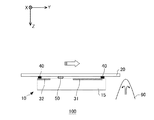
図1は、実施例1に係る半導体装置100を説明するための図である。半導体装置100は、半導体パッケージ10および実装基板20を備える。図1は、半導体パッケージ10と実装基板20とをはんだ付けするためのフロー工程を示している。
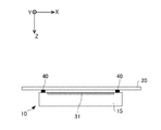
図3は、実施例2に係る半導体パッケージ10の構成の一例を示す。本例の半導体パッケージ10は、第1電極31と、第2電極32と、第1突起部41とを備える。
図4は、実施例3に係る半導体パッケージ10の構成の一例を示す。本例の半導体パッケージ10は、第1電極31と、第2電極32と、第1突起部41と、第2突起部42とを備える。本例の半導体パッケージ10は、第1突起部41の個数が実施例2に係る半導体パッケージ10と相違する。また、本例の半導体パッケージ10は、第2突起部42を備える点で、実施例2に係る半導体パッケージ10と相違する。本例では、実施例2に係る半導体パッケージ10と相違する点について特に説明する。
図5は、実施例4に係る半導体パッケージ10の構成の一例を示す。本例の半導体パッケージ10は、第1電極31と、4つの第2電極32a〜32dと、2つの第1突起部41a,41bと、1つの第2突起部42とを備える。本例の半導体パッケージ10は、第2突起部42を1つ備える点で、実施例3に係る半導体パッケージ10と相違する。本例では、実施例3に係る半導体パッケージ10と相違する点について特に説明する。
[0]
図6は、実施例5に係る半導体パッケージ10の構成の一例を示す。本例の半導体パッケージ10は、第1電極31と、4つの第2電極32a〜32dと、2つの第1突起部41a,41bと、第2突起部42とを備える。本例の半導体パッケージ10は、第2突起部42の配置が実施例4に係る半導体パッケージ10と相違する。本例では、実施例4と相違する点について特に説明する。
図7は、実施例6に係る半導体パッケージ10の構成の一例を示す。本例の半導体パッケージ10は、第1電極31と、4つの第2電極32a〜32dと、4つの第1突起部41a〜41dとを備える。本例の半導体パッケージ10は、第2突起部42の配置および形状が実施例2に係る半導体パッケージ10と相違する。本例では、実施例2に係る半導体パッケージ10と相違する点について特に説明する。
Claims (16)
- 半導体チップを含む半導体パッケージであって、
パッケージ本体と、
前記パッケージ本体の底面において露出した複数の電極と、
前記パッケージ本体の底面から、前記複数の電極よりも突出した突起部と
を備え、
前記突起部は、前記複数の電極のうち、最も間隔の狭い2つの電極が配列された第1方向と異なる第2方向において、当該2つの電極と重ならないように配置され、
前記複数の電極は、
前記第2方向において前記突起部と重なる第1電極と、
前記第1電極よりも露出面積が小さく、前記第2方向において前記突起部と重ならない第2電極と
を有する
半導体パッケージ。 - 半導体チップを含む半導体パッケージであって、
パッケージ本体と、
前記パッケージ本体の底面において露出した複数の電極と、
前記パッケージ本体の底面から、前記複数の電極よりも突出した突起部と
を備え、
前記突起部は、前記複数の電極のうち、前記半導体パッケージの端部に設けられた最も間隔の狭い2つの電極が配列された第1方向と異なる第2方向において、当該2つの電極と重ならないように配置されている
半導体パッケージ。 - 複数の前記突起部を備え、
複数の前記突起部は、前記第2方向において、前記2つの電極と重ならないように配置されている
請求項1又は2に記載の半導体パッケージ。 - 前記複数の電極は、
前記第2方向において前記突起部と重なる第1電極と、
前記第1電極よりも露出面積が小さく、前記第2方向において前記突起部と重ならない第2電極と
を有する
請求項2に記載の半導体パッケージ。 - 前記突起部は、
前記パッケージ本体の底面の角に配置された第1突起部と、
前記第1電極と前記第2電極との間に配置された第2突起部と
を有する
請求項4に記載の半導体パッケージ。 - 前記第1方向に配列された複数の前記第2電極を備え、
前記第2突起部の前記第1方向における幅が、複数の前記第2電極の前記第1方向における間隔と同一である
請求項5に記載の半導体パッケージ。 - 前記第2突起部の前記第1方向における幅が、前記第1突起部の前記第1方向における幅よりも大きい
請求項5又は6に記載の半導体パッケージ。 - 前記第2突起部の前記第2方向における幅は、前記第2突起部の前記第1方向における幅よりも大きい
請求項5から7のいずれか一項に記載の半導体パッケージ。 - 前記第2方向における前記第1電極と前記第2突起部との間の距離L1は、前記第2方向における前記第2電極と前記第2突起部との間の距離L2よりも小さい
請求項5から8のいずれか一項に記載の半導体パッケージ。 - 前記第2方向における前記第1電極と前記第2突起部との間の距離L1は、前記第2方向における前記第2電極と前記第2突起部との間の距離L2よりも大きい
請求項5から8のいずれか一項に記載の半導体パッケージ。 - 前記突起部の先端が丸みを有する
請求項1から10のいずれか一項に記載の半導体パッケージ。 - 前記突起部の平面形状が丸みを有する
請求項1から11のいずれか一項に記載の半導体パッケージ。 - 請求項1から12のいずれか一項に記載の半導体パッケージと、
前記半導体パッケージが取り付けられた実装基板と、
前記実装基板と前記半導体パッケージとの間に設けられたはんだと
を備える半導体装置。 - パッケージ本体と、前記パッケージ本体の底面において露出した複数の電極と、前記複数の電極のうち、最も間隔の狭い2つの電極が配列された第1方向と異なる第2方向において、当該2つの電極と重ならないように配置され、前記複数の電極よりも突出した突起部とを備える半導体パッケージを用意する段階と、
前記半導体パッケージと実装基板とを仮止めする段階と、
前記半導体パッケージと前記実装基板との間にはんだを流す段階と
を備え、
前記複数の電極は、
前記第2方向において前記突起部と重なる第1電極と、
前記第1電極よりも露出面積が小さく、前記第2方向において前記突起部と重ならない第2電極と
を有する
半導体装置の製造方法。 - パッケージ本体と、前記パッケージ本体の底面において露出した複数の電極と、前記複数の電極のうち、半導体パッケージの端部に設けられた最も間隔の狭い2つの電極が配列された第1方向と異なる第2方向において、当該2つの電極と重ならないように配置され、前記複数の電極よりも突出した突起部とを備える半導体パッケージを用意する段階と、
前記半導体パッケージと実装基板とを仮止めする段階と、
前記半導体パッケージと前記実装基板との間にはんだを流す段階と
を備える
半導体装置の製造方法。 - 前記はんだを流す段階において、前記半導体パッケージが前記第2方向に移動する
請求項14又は15に記載の半導体装置の製造方法。
Priority Applications (4)
| Application Number | Priority Date | Filing Date | Title |
|---|---|---|---|
| JP2017111214A JP6984183B2 (ja) | 2017-06-05 | 2017-06-05 | 半導体パッケージ、半導体装置および半導体装置の製造方法 |
| CN201810177954.8A CN108987353B (zh) | 2017-06-05 | 2018-03-05 | 半导体封装件、半导体装置以及半导体装置的制造方法 |
| US15/914,990 US10607906B2 (en) | 2017-06-05 | 2018-03-07 | Semiconductor package, semiconductor device and semiconductor device manufacturing method |
| TW107107816A TWI745558B (zh) | 2017-06-05 | 2018-03-08 | 半導體封裝、半導體裝置及半導體裝置之製造方法 |
Applications Claiming Priority (1)
| Application Number | Priority Date | Filing Date | Title |
|---|---|---|---|
| JP2017111214A JP6984183B2 (ja) | 2017-06-05 | 2017-06-05 | 半導体パッケージ、半導体装置および半導体装置の製造方法 |
Publications (3)
| Publication Number | Publication Date |
|---|---|
| JP2018206977A JP2018206977A (ja) | 2018-12-27 |
| JP2018206977A5 JP2018206977A5 (ja) | 2020-07-16 |
| JP6984183B2 true JP6984183B2 (ja) | 2021-12-17 |
Family
ID=64460337
Family Applications (1)
| Application Number | Title | Priority Date | Filing Date |
|---|---|---|---|
| JP2017111214A Active JP6984183B2 (ja) | 2017-06-05 | 2017-06-05 | 半導体パッケージ、半導体装置および半導体装置の製造方法 |
Country Status (4)
| Country | Link |
|---|---|
| US (1) | US10607906B2 (ja) |
| JP (1) | JP6984183B2 (ja) |
| CN (1) | CN108987353B (ja) |
| TW (1) | TWI745558B (ja) |
Family Cites Families (19)
| Publication number | Priority date | Publication date | Assignee | Title |
|---|---|---|---|---|
| JPH03147353A (ja) | 1989-11-02 | 1991-06-24 | New Japan Radio Co Ltd | 表面実装型半導体パッケージ |
| US5220200A (en) * | 1990-12-10 | 1993-06-15 | Delco Electronics Corporation | Provision of substrate pillars to maintain chip standoff |
| US5186383A (en) * | 1991-10-02 | 1993-02-16 | Motorola, Inc. | Method for forming solder bump interconnections to a solder-plated circuit trace |
| US5269453A (en) * | 1992-04-02 | 1993-12-14 | Motorola, Inc. | Low temperature method for forming solder bump interconnections to a plated circuit trace |
| JPH07249707A (ja) | 1994-03-09 | 1995-09-26 | Fujitsu Ltd | 半導体パッケージ |
| JP2944449B2 (ja) * | 1995-02-24 | 1999-09-06 | 日本電気株式会社 | 半導体パッケージとその製造方法 |
| US5796169A (en) * | 1996-11-19 | 1998-08-18 | International Business Machines Corporation | Structurally reinforced ball grid array semiconductor package and systems |
| JP2006210956A (ja) | 1997-02-27 | 2006-08-10 | Fujitsu Ltd | 半導体装置 |
| US6118182A (en) * | 1998-06-25 | 2000-09-12 | Intel Corporation | Integrated circuit package with rectangular contact pads |
| US6122171A (en) * | 1999-07-30 | 2000-09-19 | Micron Technology, Inc. | Heat sink chip package and method of making |
| US6531335B1 (en) * | 2000-04-28 | 2003-03-11 | Micron Technology, Inc. | Interposers including upwardly protruding dams, semiconductor device assemblies including the interposers, and methods |
| US7041533B1 (en) * | 2000-06-08 | 2006-05-09 | Micron Technology, Inc. | Stereolithographic method for fabricating stabilizers for semiconductor devices |
| JP3942457B2 (ja) * | 2002-02-27 | 2007-07-11 | Necエレクトロニクス株式会社 | 電子部品の製造方法 |
| US20060108678A1 (en) * | 2002-05-07 | 2006-05-25 | Microfabrica Inc. | Probe arrays and method for making |
| CN100587930C (zh) * | 2005-05-17 | 2010-02-03 | 松下电器产业株式会社 | 倒装片安装体及倒装片安装方法 |
| US20090085227A1 (en) * | 2005-05-17 | 2009-04-02 | Matsushita Electric Industrial Co., Ltd. | Flip-chip mounting body and flip-chip mounting method |
| WO2007039960A1 (ja) * | 2005-10-05 | 2007-04-12 | Sharp Kabushiki Kaisha | 配線基板及びそれを備えた表示装置 |
| JP2007123443A (ja) * | 2005-10-26 | 2007-05-17 | Shinko Electric Ind Co Ltd | 回路基板、半導体装置、及び半導体装置の製造方法 |
| JP4752586B2 (ja) * | 2006-04-12 | 2011-08-17 | ソニー株式会社 | 半導体装置の製造方法 |
-
2017
- 2017-06-05 JP JP2017111214A patent/JP6984183B2/ja active Active
-
2018
- 2018-03-05 CN CN201810177954.8A patent/CN108987353B/zh active Active
- 2018-03-07 US US15/914,990 patent/US10607906B2/en active Active
- 2018-03-08 TW TW107107816A patent/TWI745558B/zh active
Also Published As
| Publication number | Publication date |
|---|---|
| TW201903978A (zh) | 2019-01-16 |
| TWI745558B (zh) | 2021-11-11 |
| CN108987353B (zh) | 2023-10-24 |
| JP2018206977A (ja) | 2018-12-27 |
| US10607906B2 (en) | 2020-03-31 |
| CN108987353A (zh) | 2018-12-11 |
| US20180350705A1 (en) | 2018-12-06 |
Similar Documents
| Publication | Publication Date | Title |
|---|---|---|
| JP4536603B2 (ja) | 半導体装置の製造方法及び半導体装置用実装基板及び半導体装置 | |
| JP2007134540A (ja) | 半導体装置およびその製造方法 | |
| JP6984183B2 (ja) | 半導体パッケージ、半導体装置および半導体装置の製造方法 | |
| JP2007165832A (ja) | 電子部品の実装構造、及びその実装方法 | |
| JP4976673B2 (ja) | 半導体装置、基板及び半導体装置の製造方法 | |
| KR102408126B1 (ko) | 솔더 브릿지를 억제할 수 있는 전기적 패턴을 갖는 전기적 장치 | |
| US9595488B2 (en) | Semiconductor device | |
| JP5062376B1 (ja) | 電子部品実装基板の製造方法 | |
| JP6706994B2 (ja) | 基板、半導体モジュール、および、半導体モジュールの製造方法 | |
| JP2019009216A (ja) | 半導体装置の製造方法および半導体装置 | |
| JP7074621B2 (ja) | 半導体装置及びその製造方法 | |
| KR101216850B1 (ko) | 카메라 모듈용 인쇄회로기판 | |
| JP4735352B2 (ja) | 電子部品の配置構造及び配置方法 | |
| JP2008091758A (ja) | 半導体装置およびその製造方法 | |
| JP5741458B2 (ja) | 半導体パッケージの実装方法 | |
| JP2004319692A (ja) | 電子回路基板 | |
| JP2013254797A (ja) | 表面実装素子 | |
| JP2006253165A (ja) | 半導体装置および半導体装置の製造方法 | |
| TWI249824B (en) | Semiconductor package with passive component | |
| JP2010080732A (ja) | 半導体モジュールおよびその製造方法 | |
| JP2017195290A (ja) | 基板構造 | |
| JP2004342712A (ja) | 半導体装置の製造方法 | |
| JP2006049528A (ja) | 半導体装置および半導体装置の製造方法 | |
| JPH08330714A (ja) | 半導体フラットパッケージの表面実装方法及び半導体フラットパッケージ用実装配線板 |
Legal Events
| Date | Code | Title | Description |
|---|---|---|---|
| A621 | Written request for application examination |
Free format text: JAPANESE INTERMEDIATE CODE: A621 Effective date: 20200514 |
|
| A521 | Request for written amendment filed |
Free format text: JAPANESE INTERMEDIATE CODE: A523 Effective date: 20200608 |
|
| A977 | Report on retrieval |
Free format text: JAPANESE INTERMEDIATE CODE: A971007 Effective date: 20210524 |
|
| A131 | Notification of reasons for refusal |
Free format text: JAPANESE INTERMEDIATE CODE: A131 Effective date: 20210601 |
|
| A521 | Request for written amendment filed |
Free format text: JAPANESE INTERMEDIATE CODE: A523 Effective date: 20210716 |
|
| TRDD | Decision of grant or rejection written | ||
| A01 | Written decision to grant a patent or to grant a registration (utility model) |
Free format text: JAPANESE INTERMEDIATE CODE: A01 Effective date: 20211026 |
|
| A61 | First payment of annual fees (during grant procedure) |
Free format text: JAPANESE INTERMEDIATE CODE: A61 Effective date: 20211108 |
|
| R150 | Certificate of patent or registration of utility model |
Ref document number: 6984183 Country of ref document: JP Free format text: JAPANESE INTERMEDIATE CODE: R150 |