JP6976686B2 - エッジリング特性評価を実行するためのシステムおよび方法 - Google Patents
エッジリング特性評価を実行するためのシステムおよび方法 Download PDFInfo
- Publication number
- JP6976686B2 JP6976686B2 JP2017006322A JP2017006322A JP6976686B2 JP 6976686 B2 JP6976686 B2 JP 6976686B2 JP 2017006322 A JP2017006322 A JP 2017006322A JP 2017006322 A JP2017006322 A JP 2017006322A JP 6976686 B2 JP6976686 B2 JP 6976686B2
- Authority
- JP
- Japan
- Prior art keywords
- edge ring
- substrate
- contact
- inner portion
- support
- Prior art date
- Legal status (The legal status is an assumption and is not a legal conclusion. Google has not performed a legal analysis and makes no representation as to the accuracy of the status listed.)
- Active
Links
Images


Classifications
-
- H—ELECTRICITY
- H01—ELECTRIC ELEMENTS
- H01L—SEMICONDUCTOR DEVICES NOT COVERED BY CLASS H10
- H01L21/00—Processes or apparatus adapted for the manufacture or treatment of semiconductor or solid state devices or of parts thereof
- H01L21/02—Manufacture or treatment of semiconductor devices or of parts thereof
- H01L21/04—Manufacture or treatment of semiconductor devices or of parts thereof the devices having at least one potential-jump barrier or surface barrier, e.g. PN junction, depletion layer or carrier concentration layer
- H01L21/18—Manufacture or treatment of semiconductor devices or of parts thereof the devices having at least one potential-jump barrier or surface barrier, e.g. PN junction, depletion layer or carrier concentration layer the devices having semiconductor bodies comprising elements of Group IV of the Periodic System or AIIIBV compounds with or without impurities, e.g. doping materials
- H01L21/30—Treatment of semiconductor bodies using processes or apparatus not provided for in groups H01L21/20 - H01L21/26
- H01L21/302—Treatment of semiconductor bodies using processes or apparatus not provided for in groups H01L21/20 - H01L21/26 to change their surface-physical characteristics or shape, e.g. etching, polishing, cutting
- H01L21/306—Chemical or electrical treatment, e.g. electrolytic etching
- H01L21/3065—Plasma etching; Reactive-ion etching
-
- H—ELECTRICITY
- H01—ELECTRIC ELEMENTS
- H01J—ELECTRIC DISCHARGE TUBES OR DISCHARGE LAMPS
- H01J37/00—Discharge tubes with provision for introducing objects or material to be exposed to the discharge, e.g. for the purpose of examination or processing thereof
- H01J37/32—Gas-filled discharge tubes
- H01J37/32431—Constructional details of the reactor
- H01J37/32623—Mechanical discharge control means
- H01J37/32642—Focus rings
-
- H—ELECTRICITY
- H01—ELECTRIC ELEMENTS
- H01J—ELECTRIC DISCHARGE TUBES OR DISCHARGE LAMPS
- H01J37/00—Discharge tubes with provision for introducing objects or material to be exposed to the discharge, e.g. for the purpose of examination or processing thereof
- H01J37/32—Gas-filled discharge tubes
- H01J37/32431—Constructional details of the reactor
- H01J37/32715—Workpiece holder
-
- H—ELECTRICITY
- H01—ELECTRIC ELEMENTS
- H01J—ELECTRIC DISCHARGE TUBES OR DISCHARGE LAMPS
- H01J37/00—Discharge tubes with provision for introducing objects or material to be exposed to the discharge, e.g. for the purpose of examination or processing thereof
- H01J37/32—Gas-filled discharge tubes
- H01J37/32009—Arrangements for generation of plasma specially adapted for examination or treatment of objects, e.g. plasma sources
- H01J37/32082—Radio frequency generated discharge
- H01J37/321—Radio frequency generated discharge the radio frequency energy being inductively coupled to the plasma
-
- H—ELECTRICITY
- H01—ELECTRIC ELEMENTS
- H01J—ELECTRIC DISCHARGE TUBES OR DISCHARGE LAMPS
- H01J37/00—Discharge tubes with provision for introducing objects or material to be exposed to the discharge, e.g. for the purpose of examination or processing thereof
- H01J37/32—Gas-filled discharge tubes
- H01J37/32009—Arrangements for generation of plasma specially adapted for examination or treatment of objects, e.g. plasma sources
- H01J37/32082—Radio frequency generated discharge
- H01J37/32174—Circuits specially adapted for controlling the RF discharge
- H01J37/32183—Matching circuits
-
- H—ELECTRICITY
- H01—ELECTRIC ELEMENTS
- H01J—ELECTRIC DISCHARGE TUBES OR DISCHARGE LAMPS
- H01J37/00—Discharge tubes with provision for introducing objects or material to be exposed to the discharge, e.g. for the purpose of examination or processing thereof
- H01J37/32—Gas-filled discharge tubes
- H01J37/32431—Constructional details of the reactor
- H01J37/32798—Further details of plasma apparatus not provided for in groups H01J37/3244 - H01J37/32788; special provisions for cleaning or maintenance of the apparatus
- H01J37/3288—Maintenance
-
- H—ELECTRICITY
- H01—ELECTRIC ELEMENTS
- H01L—SEMICONDUCTOR DEVICES NOT COVERED BY CLASS H10
- H01L21/00—Processes or apparatus adapted for the manufacture or treatment of semiconductor or solid state devices or of parts thereof
- H01L21/02—Manufacture or treatment of semiconductor devices or of parts thereof
- H01L21/02104—Forming layers
- H01L21/02107—Forming insulating materials on a substrate
- H01L21/02296—Forming insulating materials on a substrate characterised by the treatment performed before or after the formation of the layer
- H01L21/02299—Forming insulating materials on a substrate characterised by the treatment performed before or after the formation of the layer pre-treatment
- H01L21/02312—Forming insulating materials on a substrate characterised by the treatment performed before or after the formation of the layer pre-treatment treatment by exposure to a gas or vapour
- H01L21/02315—Forming insulating materials on a substrate characterised by the treatment performed before or after the formation of the layer pre-treatment treatment by exposure to a gas or vapour treatment by exposure to a plasma
-
- H—ELECTRICITY
- H01—ELECTRIC ELEMENTS
- H01L—SEMICONDUCTOR DEVICES NOT COVERED BY CLASS H10
- H01L21/00—Processes or apparatus adapted for the manufacture or treatment of semiconductor or solid state devices or of parts thereof
- H01L21/02—Manufacture or treatment of semiconductor devices or of parts thereof
- H01L21/04—Manufacture or treatment of semiconductor devices or of parts thereof the devices having at least one potential-jump barrier or surface barrier, e.g. PN junction, depletion layer or carrier concentration layer
- H01L21/18—Manufacture or treatment of semiconductor devices or of parts thereof the devices having at least one potential-jump barrier or surface barrier, e.g. PN junction, depletion layer or carrier concentration layer the devices having semiconductor bodies comprising elements of Group IV of the Periodic System or AIIIBV compounds with or without impurities, e.g. doping materials
- H01L21/30—Treatment of semiconductor bodies using processes or apparatus not provided for in groups H01L21/20 - H01L21/26
- H01L21/31—Treatment of semiconductor bodies using processes or apparatus not provided for in groups H01L21/20 - H01L21/26 to form insulating layers thereon, e.g. for masking or by using photolithographic techniques; After treatment of these layers; Selection of materials for these layers
- H01L21/3205—Deposition of non-insulating-, e.g. conductive- or resistive-, layers on insulating layers; After-treatment of these layers
- H01L21/321—After treatment
- H01L21/3213—Physical or chemical etching of the layers, e.g. to produce a patterned layer from a pre-deposited extensive layer
- H01L21/32133—Physical or chemical etching of the layers, e.g. to produce a patterned layer from a pre-deposited extensive layer by chemical means only
- H01L21/32135—Physical or chemical etching of the layers, e.g. to produce a patterned layer from a pre-deposited extensive layer by chemical means only by vapour etching only
- H01L21/32136—Physical or chemical etching of the layers, e.g. to produce a patterned layer from a pre-deposited extensive layer by chemical means only by vapour etching only using plasmas
-
- H—ELECTRICITY
- H01—ELECTRIC ELEMENTS
- H01L—SEMICONDUCTOR DEVICES NOT COVERED BY CLASS H10
- H01L21/00—Processes or apparatus adapted for the manufacture or treatment of semiconductor or solid state devices or of parts thereof
- H01L21/67—Apparatus specially adapted for handling semiconductor or electric solid state devices during manufacture or treatment thereof; Apparatus specially adapted for handling wafers during manufacture or treatment of semiconductor or electric solid state devices or components ; Apparatus not specifically provided for elsewhere
- H01L21/67005—Apparatus not specifically provided for elsewhere
- H01L21/67242—Apparatus for monitoring, sorting or marking
- H01L21/67259—Position monitoring, e.g. misposition detection or presence detection
-
- H—ELECTRICITY
- H01—ELECTRIC ELEMENTS
- H01L—SEMICONDUCTOR DEVICES NOT COVERED BY CLASS H10
- H01L21/00—Processes or apparatus adapted for the manufacture or treatment of semiconductor or solid state devices or of parts thereof
- H01L21/67—Apparatus specially adapted for handling semiconductor or electric solid state devices during manufacture or treatment thereof; Apparatus specially adapted for handling wafers during manufacture or treatment of semiconductor or electric solid state devices or components ; Apparatus not specifically provided for elsewhere
- H01L21/68—Apparatus specially adapted for handling semiconductor or electric solid state devices during manufacture or treatment thereof; Apparatus specially adapted for handling wafers during manufacture or treatment of semiconductor or electric solid state devices or components ; Apparatus not specifically provided for elsewhere for positioning, orientation or alignment
- H01L21/681—Apparatus specially adapted for handling semiconductor or electric solid state devices during manufacture or treatment thereof; Apparatus specially adapted for handling wafers during manufacture or treatment of semiconductor or electric solid state devices or components ; Apparatus not specifically provided for elsewhere for positioning, orientation or alignment using optical controlling means
-
- H—ELECTRICITY
- H01—ELECTRIC ELEMENTS
- H01L—SEMICONDUCTOR DEVICES NOT COVERED BY CLASS H10
- H01L21/00—Processes or apparatus adapted for the manufacture or treatment of semiconductor or solid state devices or of parts thereof
- H01L21/67—Apparatus specially adapted for handling semiconductor or electric solid state devices during manufacture or treatment thereof; Apparatus specially adapted for handling wafers during manufacture or treatment of semiconductor or electric solid state devices or components ; Apparatus not specifically provided for elsewhere
- H01L21/683—Apparatus specially adapted for handling semiconductor or electric solid state devices during manufacture or treatment thereof; Apparatus specially adapted for handling wafers during manufacture or treatment of semiconductor or electric solid state devices or components ; Apparatus not specifically provided for elsewhere for supporting or gripping
- H01L21/6835—Apparatus specially adapted for handling semiconductor or electric solid state devices during manufacture or treatment thereof; Apparatus specially adapted for handling wafers during manufacture or treatment of semiconductor or electric solid state devices or components ; Apparatus not specifically provided for elsewhere for supporting or gripping using temporarily an auxiliary support
-
- H—ELECTRICITY
- H01—ELECTRIC ELEMENTS
- H01L—SEMICONDUCTOR DEVICES NOT COVERED BY CLASS H10
- H01L21/00—Processes or apparatus adapted for the manufacture or treatment of semiconductor or solid state devices or of parts thereof
- H01L21/67—Apparatus specially adapted for handling semiconductor or electric solid state devices during manufacture or treatment thereof; Apparatus specially adapted for handling wafers during manufacture or treatment of semiconductor or electric solid state devices or components ; Apparatus not specifically provided for elsewhere
- H01L21/683—Apparatus specially adapted for handling semiconductor or electric solid state devices during manufacture or treatment thereof; Apparatus specially adapted for handling wafers during manufacture or treatment of semiconductor or electric solid state devices or components ; Apparatus not specifically provided for elsewhere for supporting or gripping
- H01L21/687—Apparatus specially adapted for handling semiconductor or electric solid state devices during manufacture or treatment thereof; Apparatus specially adapted for handling wafers during manufacture or treatment of semiconductor or electric solid state devices or components ; Apparatus not specifically provided for elsewhere for supporting or gripping using mechanical means, e.g. chucks, clamps or pinches
- H01L21/68714—Apparatus specially adapted for handling semiconductor or electric solid state devices during manufacture or treatment thereof; Apparatus specially adapted for handling wafers during manufacture or treatment of semiconductor or electric solid state devices or components ; Apparatus not specifically provided for elsewhere for supporting or gripping using mechanical means, e.g. chucks, clamps or pinches the wafers being placed on a susceptor, stage or support
- H01L21/68721—Apparatus specially adapted for handling semiconductor or electric solid state devices during manufacture or treatment thereof; Apparatus specially adapted for handling wafers during manufacture or treatment of semiconductor or electric solid state devices or components ; Apparatus not specifically provided for elsewhere for supporting or gripping using mechanical means, e.g. chucks, clamps or pinches the wafers being placed on a susceptor, stage or support characterised by edge clamping, e.g. clamping ring
-
- H—ELECTRICITY
- H01—ELECTRIC ELEMENTS
- H01L—SEMICONDUCTOR DEVICES NOT COVERED BY CLASS H10
- H01L21/00—Processes or apparatus adapted for the manufacture or treatment of semiconductor or solid state devices or of parts thereof
- H01L21/67—Apparatus specially adapted for handling semiconductor or electric solid state devices during manufacture or treatment thereof; Apparatus specially adapted for handling wafers during manufacture or treatment of semiconductor or electric solid state devices or components ; Apparatus not specifically provided for elsewhere
- H01L21/683—Apparatus specially adapted for handling semiconductor or electric solid state devices during manufacture or treatment thereof; Apparatus specially adapted for handling wafers during manufacture or treatment of semiconductor or electric solid state devices or components ; Apparatus not specifically provided for elsewhere for supporting or gripping
- H01L21/687—Apparatus specially adapted for handling semiconductor or electric solid state devices during manufacture or treatment thereof; Apparatus specially adapted for handling wafers during manufacture or treatment of semiconductor or electric solid state devices or components ; Apparatus not specifically provided for elsewhere for supporting or gripping using mechanical means, e.g. chucks, clamps or pinches
- H01L21/68714—Apparatus specially adapted for handling semiconductor or electric solid state devices during manufacture or treatment thereof; Apparatus specially adapted for handling wafers during manufacture or treatment of semiconductor or electric solid state devices or components ; Apparatus not specifically provided for elsewhere for supporting or gripping using mechanical means, e.g. chucks, clamps or pinches the wafers being placed on a susceptor, stage or support
- H01L21/68735—Apparatus specially adapted for handling semiconductor or electric solid state devices during manufacture or treatment thereof; Apparatus specially adapted for handling wafers during manufacture or treatment of semiconductor or electric solid state devices or components ; Apparatus not specifically provided for elsewhere for supporting or gripping using mechanical means, e.g. chucks, clamps or pinches the wafers being placed on a susceptor, stage or support characterised by edge profile or support profile
-
- H—ELECTRICITY
- H01—ELECTRIC ELEMENTS
- H01L—SEMICONDUCTOR DEVICES NOT COVERED BY CLASS H10
- H01L21/00—Processes or apparatus adapted for the manufacture or treatment of semiconductor or solid state devices or of parts thereof
- H01L21/67—Apparatus specially adapted for handling semiconductor or electric solid state devices during manufacture or treatment thereof; Apparatus specially adapted for handling wafers during manufacture or treatment of semiconductor or electric solid state devices or components ; Apparatus not specifically provided for elsewhere
- H01L21/683—Apparatus specially adapted for handling semiconductor or electric solid state devices during manufacture or treatment thereof; Apparatus specially adapted for handling wafers during manufacture or treatment of semiconductor or electric solid state devices or components ; Apparatus not specifically provided for elsewhere for supporting or gripping
- H01L21/687—Apparatus specially adapted for handling semiconductor or electric solid state devices during manufacture or treatment thereof; Apparatus specially adapted for handling wafers during manufacture or treatment of semiconductor or electric solid state devices or components ; Apparatus not specifically provided for elsewhere for supporting or gripping using mechanical means, e.g. chucks, clamps or pinches
- H01L21/68714—Apparatus specially adapted for handling semiconductor or electric solid state devices during manufacture or treatment thereof; Apparatus specially adapted for handling wafers during manufacture or treatment of semiconductor or electric solid state devices or components ; Apparatus not specifically provided for elsewhere for supporting or gripping using mechanical means, e.g. chucks, clamps or pinches the wafers being placed on a susceptor, stage or support
- H01L21/68742—Apparatus specially adapted for handling semiconductor or electric solid state devices during manufacture or treatment thereof; Apparatus specially adapted for handling wafers during manufacture or treatment of semiconductor or electric solid state devices or components ; Apparatus not specifically provided for elsewhere for supporting or gripping using mechanical means, e.g. chucks, clamps or pinches the wafers being placed on a susceptor, stage or support characterised by a lifting arrangement, e.g. lift pins
-
- H—ELECTRICITY
- H05—ELECTRIC TECHNIQUES NOT OTHERWISE PROVIDED FOR
- H05H—PLASMA TECHNIQUE; PRODUCTION OF ACCELERATED ELECTRICALLY-CHARGED PARTICLES OR OF NEUTRONS; PRODUCTION OR ACCELERATION OF NEUTRAL MOLECULAR OR ATOMIC BEAMS
- H05H1/00—Generating plasma; Handling plasma
- H05H1/24—Generating plasma
- H05H1/46—Generating plasma using applied electromagnetic fields, e.g. high frequency or microwave energy
Description
本願は、2016年3月29日出願の米国仮出願第62/314,659号の利益を主張する。上記の出願の開示全体が、参照によって本明細書に組み込まれる。
[適用例1]
基板処理システム内の基板支持体であって、
基板を支持するよう構成された内側部分と、
前記内側部分を囲むエッジリングと、
コントローラと、
を備え、
前記コントローラは、
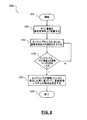
(i)前記エッジリングを上げて、前記エッジリングを前記基板と選択的に係合させること、および、(ii)前記内側部分を下げて、前記エッジリングを前記基板と選択的に係合させること、の内の少なくとも一方を実行し、
前記エッジリングが前記基板と係合した時を決定し、
前記エッジリングが前記基板と係合した時の決定に基づいて、前記基板処理システムの少なくとも1つの特性を計算する、基板支持体。
[適用例2]
適用例1に記載の基板支持体であって、前記エッジリングが前記基板と係合した時を決定することは、前記エッジリングを前記基板と係合させるために前記エッジリングが上げられた量および前記内側部分が下げられた量の少なくとも一方を決定することを含む、基板支持体。
[適用例3]
適用例1に記載の基板支持体であって、前記少なくとも1つの特性は、前記エッジリングの寸法である、基板支持体。
[適用例4]
適用例1に記載の基板支持体であって、前記基板は、前記基板の縁部から外向きに伸びる少なくとも1つの接触フィンガを備え、前記少なくとも1つの接触フィンガは、前記エッジリングと係合するよう構成されている、基板支持体。
[適用例5]
適用例4に記載の基板支持体であって、前記接触フィンガは、前記エッジリングの内径と係合するよう構成されている、基板支持体。
[適用例6]
適用例1に記載の基板支持体であって、前記エッジリングが前記基板と係合した時を決定するために、前記コントローラは、前記基板の表面から反射された信号を監視する、基板支持体。
[適用例7]
適用例1に記載の基板支持体であって、前記基板処理システムの前記少なくとも1つの特性を計算するために、前記コントローラは、前記エッジリングを前記基板と係合させるために前記エッジリングが上げられた量および前記内側部分が下げられた量の少なくとも一方を決定する、基板支持体。
[適用例8]
適用例1に記載の基板支持体であって、さらに、
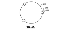
前記エッジリングを支持するために配置された複数のピンと、
前記コントローラに応答して、前記複数のピンのそれぞれを選択的に上下させるよう構成された複数のアクチュエータと、
を備える、基板支持体。
[適用例9]
適用例1に記載の基板支持体であって、さらに、
前記コントローラに応答して、前記内側部分を選択的に上下させるよう構成された少なくとも1つのアクチュエータを備える、基板支持体。
[適用例10]
基板処理システムの特性を決定する方法であって、
基板支持体の内側部分の上にテスト基板を配置する工程であって、前記テスト基板は、前記テスト基板の縁部から外向きに伸びる接触フィンガを備える、工程と、
(i)前記内側部分を囲むエッジリングを上げて、前記エッジリングの内径を前記接触フィンガと係合させること、および、(ii)前記内側部分を下げて、前記エッジリングの前記内径を前記接触フィンガと係合させること、の内の少なくとも一方を実行する工程と、
前記エッジリングの前記内径が前記接触フィンガと係合した時を決定する工程と、
前記エッジリングの前記内径が前記接触フィンガと係合した時の決定に基づいて、前記基板処理システムの少なくとも1つの特性を計算する工程と、
を備える、方法。
[適用例11]
適用例10に記載の方法であって、前記エッジリングの前記内径が前記基板と係合した時を決定する工程は、前記エッジリングの前記内径を前記基板と係合させるために前記エッジリングが上げられた量および前記内側部分が下げられた量の少なくとも一方を決定する工程を含む、方法。
[適用例12]
適用例10に記載の方法であって、前記少なくとも1つの特性は、前記エッジリングの寸法である、方法。
[適用例13]
適用例10に記載の方法であって、前記基板は、前記基板の縁部から外向きに伸びる少なくとも1つの接触フィンガを備え、前記少なくとも1つの接触フィンガは、前記エッジリングと係合するよう構成されている、方法。
[適用例14]
適用例13に記載の方法であって、前記接触フィンガは、前記エッジリングの内径と係合するよう構成されている、方法。
[適用例15]
適用例10に記載の方法であって、前記エッジリングが前記基板と係合した時を決定する工程は、前記基板の表面から反射された信号を監視する工程を含む、方法。
[適用例16]
適用例10に記載の方法であって、前記基板処理システムの前記少なくとも1つの特性を計算する工程は、前記エッジリングを前記基板と係合させるために前記エッジリングが上げられた量および前記内側部分が下げられた量の少なくとも一方を決定する工程を含む、方法。
[適用例17]
適用例10に記載の方法であって、前記エッジリングを上げる工程は、前記エッジリングを支持するために配置された複数のピンと、前記複数のピンのそれぞれを選択的に上下させるよう構成された複数のアクチュエータとを用いて、前記エッジリングを上げる工程を含む、方法。
[適用例18]
適用例10に記載の方法であって、前記内側部分を下げる工程は、前記内側部分を選択的に上下させるよう構成された少なくとも1つのアクチュエータを用いて、前記内側部分を下げる工程を含む、方法。
Claims (16)
- 基板処理システム内の基板支持体であって、
基板を支持するよう構成された内側部分と、
前記内側部分を囲むエッジリングと、
コントローラと、
を備え、
前記コントローラは、
(i)前記エッジリングを上げて、前記エッジリングを前記基板と選択的に接触させること、および、(ii)前記内側部分を下げて、前記エッジリングを前記基板と選択的に接触させること、の内の少なくとも一方を実行し、
前記エッジリングが前記基板に接触したことを示す測定信号に応答して、前記エッジリングが前記基板と接触した時を決定し、
前記エッジリングが前記基板と接触した時の決定に基づいて、前記エッジリングの厚さを計算するように構成されている、基板支持体。 - 請求項1に記載の基板支持体であって、前記エッジリングが前記基板と接触した時を決定するために、前記コントローラは、更に、前記エッジリングを前記基板と接触させるために前記エッジリングが上げられた量および前記内側部分が下げられた量の少なくとも一方を決定するように構成されている、基板支持体。
- 請求項1に記載の基板支持体であって、更に、前記基板を備え、前記基板は、前記基板の縁部から外向きに伸びる少なくとも1つの接触フィンガを備え、前記少なくとも1つの接触フィンガは、前記エッジリングと接触するよう構成されている、基板支持体。
- 請求項3に記載の基板支持体であって、前記接触フィンガは、前記エッジリングの内径と接触するよう構成されている、基板支持体。
- 請求項1に記載の基板支持体であって、前記エッジリングが前記基板と接触した時を決定するために、前記コントローラは、前記測定信号を用いて、前記基板の表面から反射された信号を監視するように構成されている、基板支持体。
- 請求項1に記載の基板支持体であって、前記エッジリングの厚さを計算するために、前記コントローラは、前記エッジリングを前記基板と接触させるために前記エッジリングが上げられた量および前記内側部分が下げられた量の少なくとも一方を決定するように構成されている、基板支持体。
- 請求項1に記載の基板支持体であって、さらに、
前記エッジリングを支持するために配置された複数のピンと、
前記コントローラに応答して、前記複数のピンのそれぞれを選択的に上下させるよう構成された複数のアクチュエータと、
を備える、基板支持体。 - 請求項1に記載の基板支持体であって、さらに、
前記コントローラに応答して、前記内側部分を選択的に上下させるよう構成された少なくとも1つのアクチュエータを備える、基板支持体。 - 基板処理システムにおけるエッジリングの厚さを決定する方法であって、
基板支持体の内側部分の上にテスト基板を配置する工程であって、前記テスト基板は、前記テスト基板の縁部から外向きに伸びる接触フィンガを備える、工程と、
(i)前記内側部分を囲むエッジリングを上げて、前記エッジリングの内径を前記接触フィンガと接触させること、および、(ii)前記内側部分を下げて、前記エッジリングの前記内径を前記接触フィンガと接触させること、の内の少なくとも一方を実行する工程と、
前記エッジリングの前記内径が前記テスト基板の前記接触フィンガに接触したことを示す測定信号に応答して、前記エッジリングの前記内径が前記接触フィンガと接触した時を決定する工程と、
前記エッジリングの前記内径が前記接触フィンガと接触した時の決定に基づいて、前記エッジリングの前記厚さを決定する工程と、
を備える、方法。 - 請求項9に記載の方法であって、前記エッジリングの前記内径が前記テスト基板と接触した時を決定する工程は、前記エッジリングの前記内径を前記テスト基板と接触させるために前記エッジリングが上げられた量および前記内側部分が下げられた量の少なくとも一方を決定する工程を含む、方法。
- 請求項9に記載の方法であって、前記テスト基板は、前記テスト基板の縁部から外向きに伸びる少なくとも1つの接触フィンガを備え、前記少なくとも1つの接触フィンガは、前記エッジリングと接触するよう構成されている、方法。
- 請求項11に記載の方法であって、前記接触フィンガは、前記エッジリングの内径と接触するよう構成されている、方法。
- 請求項9に記載の方法であって、前記エッジリングが前記テスト基板と接触した時を決定する工程は、前記測定信号を用いて、前記テスト基板の表面から反射された信号を監視する工程を含む、方法。
- 請求項9に記載の方法であって、前記エッジリングの前記厚さを決定する工程は、前記エッジリングを前記テスト基板と接触させるために前記エッジリングが上げられた量および前記内側部分が下げられた量の少なくとも一方を決定する工程を含む、方法。
- 請求項9に記載の方法であって、前記エッジリングを上げる工程は、前記エッジリングを支持するために配置された複数のピンと、前記複数のピンのそれぞれを選択的に上下させるよう構成された複数のアクチュエータとを用いて、前記エッジリングを上げる工程を含む、方法。
- 請求項9に記載の方法であって、前記内側部分を下げる工程は、前記内側部分を選択的に上下させるよう構成された少なくとも1つのアクチュエータを用いて、前記内側部分を下げる工程を含む、方法。
Applications Claiming Priority (4)
| Application Number | Priority Date | Filing Date | Title |
|---|---|---|---|
| US201662314659P | 2016-03-29 | 2016-03-29 | |
| US62/314,659 | 2016-03-29 | ||
| US15/403,786 US11011353B2 (en) | 2016-03-29 | 2017-01-11 | Systems and methods for performing edge ring characterization |
| US15/403,786 | 2017-01-11 |
Publications (3)
| Publication Number | Publication Date |
|---|---|
| JP2017183701A JP2017183701A (ja) | 2017-10-05 |
| JP2017183701A5 JP2017183701A5 (ja) | 2020-03-19 |
| JP6976686B2 true JP6976686B2 (ja) | 2021-12-08 |
Family
ID=59959706
Family Applications (1)
| Application Number | Title | Priority Date | Filing Date |
|---|---|---|---|
| JP2017006322A Active JP6976686B2 (ja) | 2016-03-29 | 2017-01-18 | エッジリング特性評価を実行するためのシステムおよび方法 |
Country Status (5)
| Country | Link |
|---|---|
| US (1) | US11011353B2 (ja) |
| JP (1) | JP6976686B2 (ja) |
| KR (1) | KR20170113014A (ja) |
| CN (2) | CN107240541B (ja) |
| TW (1) | TWI774652B (ja) |
Families Citing this family (35)
| Publication number | Priority date | Publication date | Assignee | Title |
|---|---|---|---|---|
| US10957561B2 (en) | 2015-07-30 | 2021-03-23 | Lam Research Corporation | Gas delivery system |
| US10825659B2 (en) | 2016-01-07 | 2020-11-03 | Lam Research Corporation | Substrate processing chamber including multiple gas injection points and dual injector |
| WO2017131927A1 (en) | 2016-01-26 | 2017-08-03 | Applied Materials, Inc. | Wafer edge ring lifting solution |
| US10651015B2 (en) | 2016-02-12 | 2020-05-12 | Lam Research Corporation | Variable depth edge ring for etch uniformity control |
| US10699878B2 (en) | 2016-02-12 | 2020-06-30 | Lam Research Corporation | Chamber member of a plasma source and pedestal with radially outward positioned lift pins for translation of a substrate c-ring |
| US10410832B2 (en) | 2016-08-19 | 2019-09-10 | Lam Research Corporation | Control of on-wafer CD uniformity with movable edge ring and gas injection adjustment |
| US9947517B1 (en) | 2016-12-16 | 2018-04-17 | Applied Materials, Inc. | Adjustable extended electrode for edge uniformity control |
| US10553404B2 (en) | 2017-02-01 | 2020-02-04 | Applied Materials, Inc. | Adjustable extended electrode for edge uniformity control |
| US11075105B2 (en) | 2017-09-21 | 2021-07-27 | Applied Materials, Inc. | In-situ apparatus for semiconductor process module |
| JP6966286B2 (ja) * | 2017-10-11 | 2021-11-10 | 東京エレクトロン株式会社 | プラズマ処理装置、フォーカスリングの昇降制御方法およびフォーカスリングの昇降制御プログラム |
| CN109841536A (zh) * | 2017-11-29 | 2019-06-04 | 长鑫存储技术有限公司 | 边缘补偿系统、晶圆载台系统及晶圆安装方法 |
| US11043400B2 (en) | 2017-12-21 | 2021-06-22 | Applied Materials, Inc. | Movable and removable process kit |
| JP7037964B2 (ja) * | 2018-03-09 | 2022-03-17 | 東京エレクトロン株式会社 | 測定器、及びフォーカスリングを検査するためのシステムの動作方法 |
| US10790123B2 (en) | 2018-05-28 | 2020-09-29 | Applied Materials, Inc. | Process kit with adjustable tuning ring for edge uniformity control |
| US11935773B2 (en) | 2018-06-14 | 2024-03-19 | Applied Materials, Inc. | Calibration jig and calibration method |
| KR102433436B1 (ko) | 2018-07-04 | 2022-08-17 | 삼성전자주식회사 | 기판 처리 시스템, 기판 처리 시스템에서의 에지 링 정렬 검사 방법 및 이를 수행하기 위한 원반형 비젼 센서 |
| KR20230106754A (ko) * | 2018-08-13 | 2023-07-13 | 램 리써치 코포레이션 | 에지 링 포지셔닝 및 센터링 피처들을 포함하는 플라즈마 시스 튜닝을 위한 교체가능한 에지 링 어셈블리 및/또는 접을 수 있는 에지 링 어셈블리 |
| JP7076351B2 (ja) * | 2018-10-03 | 2022-05-27 | 東京エレクトロン株式会社 | プラズマ処理装置、及びリング部材の厚さ測定方法 |
| JP2020087969A (ja) * | 2018-11-15 | 2020-06-04 | 東京エレクトロン株式会社 | プラズマ処理装置、及びリング部材の形状測定方法 |
| US11289310B2 (en) | 2018-11-21 | 2022-03-29 | Applied Materials, Inc. | Circuits for edge ring control in shaped DC pulsed plasma process device |
| JP2020115499A (ja) * | 2019-01-17 | 2020-07-30 | 東京エレクトロン株式会社 | プラズマ処理装置、及びリング部材の位置ずれ測定方法 |
| US20220146258A1 (en) * | 2019-03-06 | 2022-05-12 | Lam Research Corporation | Measurement system to measure a thickness of an adjustable edge ring for a substrate processing system |
| US11279032B2 (en) | 2019-04-11 | 2022-03-22 | Applied Materials, Inc. | Apparatus, systems, and methods for improved joint coordinate teaching accuracy of robots |
| WO2020214327A1 (en) | 2019-04-19 | 2020-10-22 | Applied Materials, Inc. | Ring removal from processing chamber |
| US10964584B2 (en) | 2019-05-20 | 2021-03-30 | Applied Materials, Inc. | Process kit ring adaptor |
| US11913777B2 (en) * | 2019-06-11 | 2024-02-27 | Applied Materials, Inc. | Detector for process kit ring wear |
| US11626305B2 (en) | 2019-06-25 | 2023-04-11 | Applied Materials, Inc. | Sensor-based correction of robot-held object |
| KR20210002175A (ko) | 2019-06-26 | 2021-01-07 | 삼성전자주식회사 | 센서 모듈 및 이를 구비하는 식각 장치 |
| CN112216646A (zh) * | 2019-07-10 | 2021-01-12 | Asm Ip私人控股有限公司 | 基板支撑组件及包括其的基板处理装置 |
| US11211269B2 (en) | 2019-07-19 | 2021-12-28 | Applied Materials, Inc. | Multi-object capable loadlock system |
| CN112701027A (zh) * | 2019-10-22 | 2021-04-23 | 夏泰鑫半导体(青岛)有限公司 | 等离子体处理装置及边缘环的更换方法 |
| US11370114B2 (en) | 2019-12-09 | 2022-06-28 | Applied Materials, Inc. | Autoteach enclosure system |
| CN111341698B (zh) * | 2020-03-09 | 2022-07-26 | 苏州能讯高能半导体有限公司 | 一种刻蚀设备 |
| USD980176S1 (en) | 2020-06-02 | 2023-03-07 | Applied Materials, Inc. | Substrate processing system carrier |
| USD954769S1 (en) | 2020-06-02 | 2022-06-14 | Applied Materials, Inc. | Enclosure system shelf |
Family Cites Families (52)
| Publication number | Priority date | Publication date | Assignee | Title |
|---|---|---|---|---|
| JP2638443B2 (ja) | 1993-08-31 | 1997-08-06 | 日本電気株式会社 | ドライエッチング方法およびドライエッチング装置 |
| US5762714A (en) | 1994-10-18 | 1998-06-09 | Applied Materials, Inc. | Plasma guard for chamber equipped with electrostatic chuck |
| JP2713276B2 (ja) | 1995-12-07 | 1998-02-16 | 日本電気株式会社 | 半導体装置の製造装置およびこれを用いた半導体装置の製造方法 |
| US6075606A (en) | 1996-02-16 | 2000-06-13 | Doan; Trung T. | Endpoint detector and method for measuring a change in wafer thickness in chemical-mechanical polishing of semiconductor wafers and other microelectronic substrates |
| US6022809A (en) | 1998-12-03 | 2000-02-08 | Taiwan Semiconductor Manufacturing Company, Ltd. | Composite shadow ring for an etch chamber and method of using |
| US6206976B1 (en) * | 1999-08-27 | 2001-03-27 | Lucent Technologies Inc. | Deposition apparatus and related method with controllable edge exclusion |
| US6589352B1 (en) | 1999-12-10 | 2003-07-08 | Applied Materials, Inc. | Self aligning non contact shadow ring process kit |
| JP2001230239A (ja) * | 2000-02-15 | 2001-08-24 | Tokyo Electron Ltd | 処理装置及び処理方法 |
| TW506234B (en) | 2000-09-18 | 2002-10-11 | Tokyo Electron Ltd | Tunable focus ring for plasma processing |
| JP3388228B2 (ja) * | 2000-12-07 | 2003-03-17 | 株式会社半導体先端テクノロジーズ | プラズマエッチング装置、及びプラズマエッチング方法 |
| US6744212B2 (en) | 2002-02-14 | 2004-06-01 | Lam Research Corporation | Plasma processing apparatus and method for confining an RF plasma under very high gas flow and RF power density conditions |
| US20040040664A1 (en) | 2002-06-03 | 2004-03-04 | Yang Jang Gyoo | Cathode pedestal for a plasma etch reactor |
| US6938505B2 (en) * | 2002-08-13 | 2005-09-06 | Taiwan Semiconductor Manufacturing Co., Ltd. | Chamber wafer detection |
| US6896765B2 (en) | 2002-09-18 | 2005-05-24 | Lam Research Corporation | Method and apparatus for the compensation of edge ring wear in a plasma processing chamber |
| US7311784B2 (en) | 2002-11-26 | 2007-12-25 | Tokyo Electron Limited | Plasma processing device |
| US6898558B2 (en) | 2002-12-31 | 2005-05-24 | Tokyo Electron Limited | Method and apparatus for monitoring a material processing system |
| US7064812B2 (en) | 2003-08-19 | 2006-06-20 | Tokyo Electron Limited | Method of using a sensor gas to determine erosion level of consumable system components |
| JP2006173223A (ja) | 2004-12-14 | 2006-06-29 | Toshiba Corp | プラズマエッチング装置およびそれを用いたプラズマエッチング方法 |
| JP4006004B2 (ja) | 2004-12-28 | 2007-11-14 | 株式会社東芝 | 半導体製造装置及び半導体装置の製造方法 |
| KR20060121362A (ko) * | 2005-05-24 | 2006-11-29 | 삼성전자주식회사 | 정전척 에지 링 측정 장치 |
| KR20080023569A (ko) | 2006-09-11 | 2008-03-14 | 주식회사 하이닉스반도체 | 식각프로파일 변형을 방지하는 플라즈마식각장치 |
| KR100783062B1 (ko) | 2006-12-27 | 2007-12-07 | 세메스 주식회사 | 기판 지지 장치, 플라즈마 식각 장치 및 플라즈마 식각방법 |
| US7968469B2 (en) | 2007-01-30 | 2011-06-28 | Applied Materials, Inc. | Method of processing a workpiece in a plasma reactor with variable height ground return path to control plasma ion density uniformity |
| US7988813B2 (en) | 2007-03-12 | 2011-08-02 | Tokyo Electron Limited | Dynamic control of process chemistry for improved within-substrate process uniformity |
| JP5317424B2 (ja) | 2007-03-28 | 2013-10-16 | 東京エレクトロン株式会社 | プラズマ処理装置 |
| US7832354B2 (en) | 2007-09-05 | 2010-11-16 | Applied Materials, Inc. | Cathode liner with wafer edge gas injection in a plasma reactor chamber |
| US7824146B2 (en) | 2007-09-07 | 2010-11-02 | Advanced Technology Development Facility | Automated systems and methods for adapting semiconductor fabrication tools to process wafers of different diameters |
| US8999106B2 (en) | 2007-12-19 | 2015-04-07 | Applied Materials, Inc. | Apparatus and method for controlling edge performance in an inductively coupled plasma chamber |
| JP2009188173A (ja) | 2008-02-06 | 2009-08-20 | Tokyo Electron Ltd | 基板処理方法及び基板処理装置 |
| JP2010034416A (ja) | 2008-07-30 | 2010-02-12 | Hitachi High-Technologies Corp | プラズマ処理装置およびプラズマ処理方法 |
| US8409995B2 (en) | 2009-08-07 | 2013-04-02 | Tokyo Electron Limited | Substrate processing apparatus, positioning method and focus ring installation method |
| JP2011210853A (ja) | 2010-03-29 | 2011-10-20 | Tokyo Electron Ltd | 消耗量測定方法 |
| JP5584517B2 (ja) | 2010-05-12 | 2014-09-03 | 東京エレクトロン株式会社 | プラズマ処理装置及び半導体装置の製造方法 |
| US8485128B2 (en) | 2010-06-30 | 2013-07-16 | Lam Research Corporation | Movable ground ring for a plasma processing chamber |
| JP6046128B2 (ja) | 2011-05-31 | 2016-12-14 | アプライド マテリアルズ インコーポレイテッドApplied Materials,Incorporated | 誘導結合プラズマ(icp)リアクタ用動的イオンラジカルシーブ及びイオンラジカルアパーチャ |
| JP5948026B2 (ja) | 2011-08-17 | 2016-07-06 | 東京エレクトロン株式会社 | 半導体製造装置及び処理方法 |
| US8933628B2 (en) | 2011-10-28 | 2015-01-13 | Applied Materials, Inc. | Inductively coupled plasma source with phase control |
| US8900469B2 (en) | 2011-12-19 | 2014-12-02 | Applied Materials, Inc. | Etch rate detection for anti-reflective coating layer and absorber layer etching |
| US20140273460A1 (en) | 2013-03-13 | 2014-09-18 | Applied Materials, Inc. | Passive control for through silicon via tilt in icp chamber |
| US10105883B2 (en) * | 2013-03-15 | 2018-10-23 | Nanonex Corporation | Imprint lithography system and method for manufacturing |
| US9425077B2 (en) | 2013-03-15 | 2016-08-23 | Taiwan Semiconductor Manufacturing Co., Ltd. | Semiconductor apparatus with transportable edge ring for substrate transport |
| CN104299929A (zh) | 2013-07-19 | 2015-01-21 | 朗姆研究公司 | 用于原位晶片边缘和背侧等离子体清洁的系统和方法 |
| CN103730318B (zh) | 2013-11-15 | 2016-04-06 | 中微半导体设备(上海)有限公司 | 一种晶圆边缘保护环及减少晶圆边缘颗粒的方法 |
| WO2015099892A1 (en) | 2013-12-23 | 2015-07-02 | Applied Materials, Inc. | Extreme edge and skew control in icp plasma reactor |
| CN104752141B (zh) | 2013-12-31 | 2017-02-08 | 中微半导体设备(上海)有限公司 | 一种等离子体处理装置及其运行方法 |
| CN104851832B (zh) | 2014-02-18 | 2018-01-19 | 北京北方华创微电子装备有限公司 | 一种固定装置、反应腔室及等离子体加工设备 |
| JP6204869B2 (ja) | 2014-04-09 | 2017-09-27 | 東京エレクトロン株式会社 | プラズマ処理装置及びプラズマ処理方法 |
| CN105336561B (zh) | 2014-07-18 | 2017-07-21 | 中微半导体设备(上海)有限公司 | 等离子体刻蚀装置 |
| US11605546B2 (en) | 2015-01-16 | 2023-03-14 | Lam Research Corporation | Moveable edge coupling ring for edge process control during semiconductor wafer processing |
| US10658222B2 (en) | 2015-01-16 | 2020-05-19 | Lam Research Corporation | Moveable edge coupling ring for edge process control during semiconductor wafer processing |
| US10438833B2 (en) * | 2016-02-16 | 2019-10-08 | Lam Research Corporation | Wafer lift ring system for wafer transfer |
| US10312121B2 (en) * | 2016-03-29 | 2019-06-04 | Lam Research Corporation | Systems and methods for aligning measurement device in substrate processing systems |
-
2017
- 2017-01-11 US US15/403,786 patent/US11011353B2/en active Active
- 2017-01-16 TW TW106101332A patent/TWI774652B/zh active
- 2017-01-17 CN CN201710036188.9A patent/CN107240541B/zh active Active
- 2017-01-17 KR KR1020170007917A patent/KR20170113014A/ko not_active Application Discontinuation
- 2017-01-17 CN CN201910856579.4A patent/CN110767525B/zh active Active
- 2017-01-18 JP JP2017006322A patent/JP6976686B2/ja active Active
Also Published As
| Publication number | Publication date |
|---|---|
| TWI774652B (zh) | 2022-08-21 |
| US20170287682A1 (en) | 2017-10-05 |
| CN107240541A (zh) | 2017-10-10 |
| CN110767525B (zh) | 2022-08-02 |
| JP2017183701A (ja) | 2017-10-05 |
| KR20170113014A (ko) | 2017-10-12 |
| TW201735235A (zh) | 2017-10-01 |
| CN107240541B (zh) | 2019-10-15 |
| US11011353B2 (en) | 2021-05-18 |
| CN110767525A (zh) | 2020-02-07 |
Similar Documents
| Publication | Publication Date | Title |
|---|---|---|
| JP6976686B2 (ja) | エッジリング特性評価を実行するためのシステムおよび方法 | |
| US11342163B2 (en) | Variable depth edge ring for etch uniformity control | |
| US20210183687A1 (en) | Edge ring arrangement with moveable edge rings | |
| US11424103B2 (en) | Control of on-wafer cd uniformity with movable edge ring and gas injection adjustment | |
| US10541168B2 (en) | Edge ring centering method using ring dynamic alignment data | |
| US11605546B2 (en) | Moveable edge coupling ring for edge process control during semiconductor wafer processing | |
| CN212874424U (zh) | 用于等离子体处理系统的边缘环和包括该边缘环的系统 | |
| US20220134568A1 (en) | Fixture for automatic calibration of substrate transfer robot | |
| US20230083737A1 (en) | System, method, and user interface for edge ring wear compensation | |
| KR20230119592A (ko) | 다운스트림 플라즈마 챔버에서 에지 라디칼 플럭스 최적화 |
Legal Events
| Date | Code | Title | Description |
|---|---|---|---|
| A521 | Request for written amendment filed |
Free format text: JAPANESE INTERMEDIATE CODE: A523 Effective date: 20170329 |
|
| A621 | Written request for application examination |
Free format text: JAPANESE INTERMEDIATE CODE: A621 Effective date: 20200115 |
|
| A521 | Request for written amendment filed |
Free format text: JAPANESE INTERMEDIATE CODE: A523 Effective date: 20200206 |
|
| A977 | Report on retrieval |
Free format text: JAPANESE INTERMEDIATE CODE: A971007 Effective date: 20210224 |
|
| A131 | Notification of reasons for refusal |
Free format text: JAPANESE INTERMEDIATE CODE: A131 Effective date: 20210330 |
|
| A521 | Request for written amendment filed |
Free format text: JAPANESE INTERMEDIATE CODE: A523 Effective date: 20210622 |
|
| TRDD | Decision of grant or rejection written | ||
| A01 | Written decision to grant a patent or to grant a registration (utility model) |
Free format text: JAPANESE INTERMEDIATE CODE: A01 Effective date: 20211012 |
|
| A61 | First payment of annual fees (during grant procedure) |
Free format text: JAPANESE INTERMEDIATE CODE: A61 Effective date: 20211110 |
|
| R150 | Certificate of patent or registration of utility model |
Ref document number: 6976686 Country of ref document: JP Free format text: JAPANESE INTERMEDIATE CODE: R150 |