JP6906397B2 - 表示装置 - Google Patents
表示装置 Download PDFInfo
- Publication number
- JP6906397B2 JP6906397B2 JP2017155333A JP2017155333A JP6906397B2 JP 6906397 B2 JP6906397 B2 JP 6906397B2 JP 2017155333 A JP2017155333 A JP 2017155333A JP 2017155333 A JP2017155333 A JP 2017155333A JP 6906397 B2 JP6906397 B2 JP 6906397B2
- Authority
- JP
- Japan
- Prior art keywords
- insulating layer
- layer
- detection electrode
- inorganic insulating
- terminal
- Prior art date
- Legal status (The legal status is an assumption and is not a legal conclusion. Google has not performed a legal analysis and makes no representation as to the accuracy of the status listed.)
- Active
Links
Images


Classifications
-
- G—PHYSICS
- G06—COMPUTING OR CALCULATING; COUNTING
- G06F—ELECTRIC DIGITAL DATA PROCESSING
- G06F3/00—Input arrangements for transferring data to be processed into a form capable of being handled by the computer; Output arrangements for transferring data from processing unit to output unit, e.g. interface arrangements
- G06F3/01—Input arrangements or combined input and output arrangements for interaction between user and computer
- G06F3/03—Arrangements for converting the position or the displacement of a member into a coded form
- G06F3/041—Digitisers, e.g. for touch screens or touch pads, characterised by the transducing means
- G06F3/044—Digitisers, e.g. for touch screens or touch pads, characterised by the transducing means by capacitive means
- G06F3/0445—Digitisers, e.g. for touch screens or touch pads, characterised by the transducing means by capacitive means using two or more layers of sensing electrodes, e.g. using two layers of electrodes separated by a dielectric layer
-
- G—PHYSICS
- G06—COMPUTING OR CALCULATING; COUNTING
- G06F—ELECTRIC DIGITAL DATA PROCESSING
- G06F3/00—Input arrangements for transferring data to be processed into a form capable of being handled by the computer; Output arrangements for transferring data from processing unit to output unit, e.g. interface arrangements
- G06F3/01—Input arrangements or combined input and output arrangements for interaction between user and computer
- G06F3/03—Arrangements for converting the position or the displacement of a member into a coded form
- G06F3/041—Digitisers, e.g. for touch screens or touch pads, characterised by the transducing means
- G06F3/0412—Digitisers structurally integrated in a display
-
- G—PHYSICS
- G06—COMPUTING OR CALCULATING; COUNTING
- G06F—ELECTRIC DIGITAL DATA PROCESSING
- G06F3/00—Input arrangements for transferring data to be processed into a form capable of being handled by the computer; Output arrangements for transferring data from processing unit to output unit, e.g. interface arrangements
- G06F3/01—Input arrangements or combined input and output arrangements for interaction between user and computer
- G06F3/03—Arrangements for converting the position or the displacement of a member into a coded form
- G06F3/041—Digitisers, e.g. for touch screens or touch pads, characterised by the transducing means
- G06F3/0416—Control or interface arrangements specially adapted for digitisers
- G06F3/04164—Connections between sensors and controllers, e.g. routing lines between electrodes and connection pads
-
- G—PHYSICS
- G06—COMPUTING OR CALCULATING; COUNTING
- G06F—ELECTRIC DIGITAL DATA PROCESSING
- G06F3/00—Input arrangements for transferring data to be processed into a form capable of being handled by the computer; Output arrangements for transferring data from processing unit to output unit, e.g. interface arrangements
- G06F3/01—Input arrangements or combined input and output arrangements for interaction between user and computer
- G06F3/03—Arrangements for converting the position or the displacement of a member into a coded form
- G06F3/041—Digitisers, e.g. for touch screens or touch pads, characterised by the transducing means
- G06F3/044—Digitisers, e.g. for touch screens or touch pads, characterised by the transducing means by capacitive means
- G06F3/0446—Digitisers, e.g. for touch screens or touch pads, characterised by the transducing means by capacitive means using a grid-like structure of electrodes in at least two directions, e.g. using row and column electrodes
-
- G—PHYSICS
- G09—EDUCATION; CRYPTOGRAPHY; DISPLAY; ADVERTISING; SEALS
- G09F—DISPLAYING; ADVERTISING; SIGNS; LABELS OR NAME-PLATES; SEALS
- G09F9/00—Indicating arrangements for variable information in which the information is built-up on a support by selection or combination of individual elements
- G09F9/30—Indicating arrangements for variable information in which the information is built-up on a support by selection or combination of individual elements in which the desired character or characters are formed by combining individual elements
-
- H—ELECTRICITY
- H05—ELECTRIC TECHNIQUES NOT OTHERWISE PROVIDED FOR
- H05B—ELECTRIC HEATING; ELECTRIC LIGHT SOURCES NOT OTHERWISE PROVIDED FOR; CIRCUIT ARRANGEMENTS FOR ELECTRIC LIGHT SOURCES, IN GENERAL
- H05B33/00—Electroluminescent light sources
- H05B33/02—Details
- H05B33/04—Sealing arrangements, e.g. against humidity
-
- H—ELECTRICITY
- H05—ELECTRIC TECHNIQUES NOT OTHERWISE PROVIDED FOR
- H05B—ELECTRIC HEATING; ELECTRIC LIGHT SOURCES NOT OTHERWISE PROVIDED FOR; CIRCUIT ARRANGEMENTS FOR ELECTRIC LIGHT SOURCES, IN GENERAL
- H05B33/00—Electroluminescent light sources
- H05B33/02—Details
- H05B33/06—Electrode terminals
-
- H—ELECTRICITY
- H05—ELECTRIC TECHNIQUES NOT OTHERWISE PROVIDED FOR
- H05B—ELECTRIC HEATING; ELECTRIC LIGHT SOURCES NOT OTHERWISE PROVIDED FOR; CIRCUIT ARRANGEMENTS FOR ELECTRIC LIGHT SOURCES, IN GENERAL
- H05B33/00—Electroluminescent light sources
- H05B33/10—Apparatus or processes specially adapted to the manufacture of electroluminescent light sources
-
- H—ELECTRICITY
- H05—ELECTRIC TECHNIQUES NOT OTHERWISE PROVIDED FOR
- H05B—ELECTRIC HEATING; ELECTRIC LIGHT SOURCES NOT OTHERWISE PROVIDED FOR; CIRCUIT ARRANGEMENTS FOR ELECTRIC LIGHT SOURCES, IN GENERAL
- H05B33/00—Electroluminescent light sources
- H05B33/12—Light sources with substantially two-dimensional [2D] radiating surfaces
- H05B33/22—Light sources with substantially two-dimensional [2D] radiating surfaces characterised by the chemical or physical composition or the arrangement of auxiliary dielectric or reflective layers
-
- H—ELECTRICITY
- H10—SEMICONDUCTOR DEVICES; ELECTRIC SOLID-STATE DEVICES NOT OTHERWISE PROVIDED FOR
- H10K—ORGANIC ELECTRIC SOLID-STATE DEVICES
- H10K50/00—Organic light-emitting devices
- H10K50/80—Constructional details
- H10K50/84—Passivation; Containers; Encapsulations
- H10K50/844—Encapsulations
-
- H—ELECTRICITY
- H10—SEMICONDUCTOR DEVICES; ELECTRIC SOLID-STATE DEVICES NOT OTHERWISE PROVIDED FOR
- H10K—ORGANIC ELECTRIC SOLID-STATE DEVICES
- H10K59/00—Integrated devices, or assemblies of multiple devices, comprising at least one organic light-emitting element covered by group H10K50/00
- H10K59/10—OLED displays
- H10K59/12—Active-matrix OLED [AMOLED] displays
- H10K59/131—Interconnections, e.g. wiring lines or terminals
-
- H—ELECTRICITY
- H10—SEMICONDUCTOR DEVICES; ELECTRIC SOLID-STATE DEVICES NOT OTHERWISE PROVIDED FOR
- H10K—ORGANIC ELECTRIC SOLID-STATE DEVICES
- H10K59/00—Integrated devices, or assemblies of multiple devices, comprising at least one organic light-emitting element covered by group H10K50/00
- H10K59/40—OLEDs integrated with touch screens
-
- H—ELECTRICITY
- H10—SEMICONDUCTOR DEVICES; ELECTRIC SOLID-STATE DEVICES NOT OTHERWISE PROVIDED FOR
- H10K—ORGANIC ELECTRIC SOLID-STATE DEVICES
- H10K59/00—Integrated devices, or assemblies of multiple devices, comprising at least one organic light-emitting element covered by group H10K50/00
- H10K59/80—Constructional details
- H10K59/87—Passivation; Containers; Encapsulations
- H10K59/873—Encapsulations
- H10K59/8731—Encapsulations multilayered coatings having a repetitive structure, e.g. having multiple organic-inorganic bilayers
-
- G—PHYSICS
- G06—COMPUTING OR CALCULATING; COUNTING
- G06F—ELECTRIC DIGITAL DATA PROCESSING
- G06F2203/00—Indexing scheme relating to G06F3/00 - G06F3/048
- G06F2203/041—Indexing scheme relating to G06F3/041 - G06F3/045
- G06F2203/04103—Manufacturing, i.e. details related to manufacturing processes specially suited for touch sensitive devices
-
- G—PHYSICS
- G06—COMPUTING OR CALCULATING; COUNTING
- G06F—ELECTRIC DIGITAL DATA PROCESSING
- G06F2203/00—Indexing scheme relating to G06F3/00 - G06F3/048
- G06F2203/041—Indexing scheme relating to G06F3/041 - G06F3/045
- G06F2203/04112—Electrode mesh in capacitive digitiser: electrode for touch sensing is formed of a mesh of very fine, normally metallic, interconnected lines that are almost invisible to see. This provides a quite large but transparent electrode surface, without need for ITO or similar transparent conductive material
-
- H—ELECTRICITY
- H10—SEMICONDUCTOR DEVICES; ELECTRIC SOLID-STATE DEVICES NOT OTHERWISE PROVIDED FOR
- H10K—ORGANIC ELECTRIC SOLID-STATE DEVICES
- H10K71/00—Manufacture or treatment specially adapted for the organic devices covered by this subclass
Landscapes
- Engineering & Computer Science (AREA)
- Theoretical Computer Science (AREA)
- General Engineering & Computer Science (AREA)
- Physics & Mathematics (AREA)
- General Physics & Mathematics (AREA)
- Human Computer Interaction (AREA)
- Inorganic Chemistry (AREA)
- Chemical & Material Sciences (AREA)
- Microelectronics & Electronic Packaging (AREA)
- Devices For Indicating Variable Information By Combining Individual Elements (AREA)
- Manufacturing & Machinery (AREA)
- Computer Networks & Wireless Communication (AREA)
- Optics & Photonics (AREA)
- Electroluminescent Light Sources (AREA)
Description
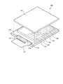
図1は、本発明の一実施形態に係る表示装置100を示す斜視図である。表示装置100は、絶縁表面を有する基板102の一主面に画素部104、タッチセンサ108が配置されている。画素部104は、複数の画素106が配置される。複数の画素106は、画素部104において、例えば、行方向及び列方向に配列される。タッチセンサ108は、画素部104に重ねて配置される。別言すれば、タッチセンサ108は、複数の画素106と重なるように配置される。タッチセンサ108は、複数の検出電極107がマトリクス状に配置され、それぞれが行方向あるいは列方向に接続される。なお、ここでは画素106およびタッチセンサ108は模式的に表現されており、その大小関係は図1記載の限りではない。
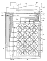
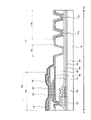
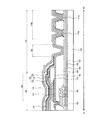
図8は、本実施形態に係る表示装置200の周辺領域の構成を示す平面図であり、図9は、本実施形態に係る表示装置200の構成を示す断面図である。図8及び図9に示す表示装置200は、第1実施形態にかかる表示装置100と異なり、第1検出電極134と第1配線136とを接続する開口部133が、開口領域120の外側に設けられている。本実施形態では、第1配線136は、開口領域120を横断して開口部133まで延長されている。
ただし、第1検出電極134と第2検出電極140とは、少なくとも第2無機絶縁層132によって絶縁されていれば足りるため、本実施形態においても表示装置100と同様に第1検出電極134が、第1無機絶縁層128と有機絶縁層130との間に設けられていてもよい。
図10は、本実施形態に係る表示装置300の周辺領域の構成を示す平面図であり、図11は、本実施形態に係る表示装置300の構成を示す断面図である。図10及び図11に示す表示装置300は、第1実施形態にかかる表示装置100と異なり、開口領域120が、第2端子115a、115bの外側に設けられており、かつ、第1検出電極134と第1配線136とを接続する開口部133が、第2端子115a、115bの内側に設けられている。表示装置300のその他の構成は表示装置100と同様である。
Claims (9)
- 絶縁表面を有する基板と、
前記絶縁表面に配置された複数の画素が配列する画素部と、
前記絶縁表面上で前記画素部の外側の領域に配置される第1端子と、前記第1端子より内側の領域に配置された第2端子と、を含む端子部と、
前記画素部と前記端子部との間に配置される第1配線を含む配線部と、
前記画素部に重ねて配置されたセンシング部と、
前記画素部及び前記配線部を覆う封止部と、を含み、
前記封止部は、
第1無機絶縁層、有機絶縁層、及び第2無機絶縁層を前記基板側からこの順で含み、
前記有機絶縁層は前記画素部と重なる領域に配置され、前記第1無機絶縁層及び前記第2無機絶縁層は前記画素部及び前記配線部と重なる領域に配置され、
前記基板と前記第1無機絶縁層との間に層間絶縁膜を含み、
前記センシング部は、
前記第1無機絶縁層より上層側であって、前記第2無機絶縁層より下層側に配置された第1検出電極と、
前記第2無機絶縁層の上層側に配置された第2検出電極と、を含み、
前記配線部は、
前記第1配線が、前記第2無機絶縁層に設けられた開口部で、前記第1検出電極と電気的に接続され、かつ、前記第2無機絶縁層の外側領域に延伸して、前記第2端子と電気的に接続され、
前記層間絶縁膜は、前記第1端子と前記第2端子との間に、前記層間絶縁膜を貫通する開口領域を有することを特徴とする表示装置。 - 前記第1検出電極は、前記第1無機絶縁層と前記有機絶縁層との間に配置される、請求項1に記載の表示装置。
- 前記第1検出電極は、前記有機絶縁層と前記第2無機絶縁層との間に配置される、請求項1に記載の表示装置。
- 前記層間絶縁膜は、前記第2端子と前記開口部との間に、前記層間絶縁膜を貫通する開口領域をさらに有する、請求項1から請求項3のいずれか一つに記載の表示装置。
- 前記基板と前記第1無機絶縁層との間に層間絶縁膜を含み、
前記層間絶縁膜は、前記開口部と前記画素部との間に、前記層間絶縁膜を貫通する開口領域をさらに有する、請求項1から請求項3のいずれか一つに記載の表示装置。 - 前記第1検出電極及び前記第2検出電極は、いずれも、チタン層、アルミニウム層及びチタン層を含む積層構造を有するメッシュ配線で形成されることを特徴とする請求項1に記載の表示装置。
- 前記第1検出電極は、チタン層、アルミニウム層及びチタン層を含む積層構造を有するメッシュ配線で形成され、前記第2検出電極は、透明電極からなるダイヤモンド電極であることを特徴とする請求項1に記載の表示装置。
- 前記第1検出電極は、透明電極からなるダイヤモンド電極であり、前記第2検出電極は、チタン層、アルミニウム層及びチタン層を含む積層構造を有するメッシュ配線で形成されることを特徴とする請求項1に記載の表示装置。
- 絶縁表面を有する基板上に複数の画素を配列した画素部を形成し、
前記絶縁表面上で前記画素部の外側の領域に第1端子を含む端子部を形成し、
前記絶縁表面上で前記画素部と前記端子部の間に第2端子を形成し、
前記画素部を覆う第1無機絶縁層を形成し、
前記第1無機絶縁層上に、第1方向に延びる第1検出電極層を形成し、
前記第1検出電極層を覆う有機絶縁層を形成し、
前記有機絶縁層を覆う第2無機絶縁層を形成し、
前記基板と前記第1無機絶縁層との間に層間絶縁膜を形成し、
前記第2端子上の前記第1無機絶縁層と前記第2無機絶縁層とを除去するとともに、前記第2無機絶縁層に前記第1検出電極層を露出する開口部を形成し、
前記第1端子と前記第2端子との間に、前記層間絶縁膜を貫通する開口領域を形成し、
前記第2無機絶縁層上に、前記第1方向と交差する方向に延びる第2検出電極層を形成するとともに、前記第2端子に接続し、前記第2無機絶縁層に設けられた開口部で、前記第1検出電極層に接続する第1配線を形成することを特徴とする表示装置の製造方法。
Priority Applications (5)
| Application Number | Priority Date | Filing Date | Title |
|---|---|---|---|
| JP2017155333A JP6906397B2 (ja) | 2017-08-10 | 2017-08-10 | 表示装置 |
| PCT/JP2018/029905 WO2019031579A1 (ja) | 2017-08-10 | 2018-08-09 | 表示装置 |
| CN201880048513.6A CN110959147B (zh) | 2017-08-10 | 2018-08-09 | 显示装置 |
| US16/773,066 US20200159356A1 (en) | 2017-08-10 | 2020-01-27 | Display device |
| JP2021107983A JP7119180B2 (ja) | 2017-08-10 | 2021-06-29 | 表示装置 |
Applications Claiming Priority (1)
| Application Number | Priority Date | Filing Date | Title |
|---|---|---|---|
| JP2017155333A JP6906397B2 (ja) | 2017-08-10 | 2017-08-10 | 表示装置 |
Related Child Applications (1)
| Application Number | Title | Priority Date | Filing Date |
|---|---|---|---|
| JP2021107983A Division JP7119180B2 (ja) | 2017-08-10 | 2021-06-29 | 表示装置 |
Publications (3)
| Publication Number | Publication Date |
|---|---|
| JP2019036016A JP2019036016A (ja) | 2019-03-07 |
| JP2019036016A5 JP2019036016A5 (ja) | 2020-09-24 |
| JP6906397B2 true JP6906397B2 (ja) | 2021-07-21 |
Family
ID=65272437
Family Applications (2)
| Application Number | Title | Priority Date | Filing Date |
|---|---|---|---|
| JP2017155333A Active JP6906397B2 (ja) | 2017-08-10 | 2017-08-10 | 表示装置 |
| JP2021107983A Active JP7119180B2 (ja) | 2017-08-10 | 2021-06-29 | 表示装置 |
Family Applications After (1)
| Application Number | Title | Priority Date | Filing Date |
|---|---|---|---|
| JP2021107983A Active JP7119180B2 (ja) | 2017-08-10 | 2021-06-29 | 表示装置 |
Country Status (4)
| Country | Link |
|---|---|
| US (1) | US20200159356A1 (ja) |
| JP (2) | JP6906397B2 (ja) |
| CN (1) | CN110959147B (ja) |
| WO (1) | WO2019031579A1 (ja) |
Families Citing this family (10)
| Publication number | Priority date | Publication date | Assignee | Title |
|---|---|---|---|---|
| JP7110764B2 (ja) * | 2017-10-17 | 2022-08-02 | 株式会社デンソー | ヒータ装置 |
| KR102819120B1 (ko) * | 2019-06-18 | 2025-06-13 | 삼성디스플레이 주식회사 | 표시 장치 |
| US11943989B2 (en) * | 2019-11-01 | 2024-03-26 | Chengdu Boe Optoelectronics Technology Co., Ltd. | Display module and display device |
| CN114442832B (zh) * | 2020-11-04 | 2024-09-17 | 宸美(厦门)光电有限公司 | 触控面板及其制造方法 |
| KR20220072017A (ko) | 2020-11-23 | 2022-06-02 | 삼성디스플레이 주식회사 | 표시 장치 및 그 제조 방법 |
| US11675448B2 (en) | 2020-12-11 | 2023-06-13 | Tpk Advanced Solutions Inc. | Touch panel and method for forming the same |
| TW202306773A (zh) | 2021-03-26 | 2023-02-16 | 日商琳得科股份有限公司 | 積層體 |
| WO2024033737A1 (ja) * | 2022-08-10 | 2024-02-15 | 株式会社半導体エネルギー研究所 | タッチパネル、及びタッチパネルの作製方法 |
| KR20240094219A (ko) | 2022-12-15 | 2024-06-25 | 삼성디스플레이 주식회사 | 표시 모듈 및 이를 포함하는 전자 장치 |
| KR20250031265A (ko) * | 2023-08-28 | 2025-03-07 | 엘지디스플레이 주식회사 | 표시 장치 및 이의 제조 방법 |
Family Cites Families (19)
| Publication number | Priority date | Publication date | Assignee | Title |
|---|---|---|---|---|
| JP5120528B2 (ja) * | 2006-03-29 | 2013-01-16 | カシオ計算機株式会社 | 表示装置の製造方法 |
| KR100838082B1 (ko) * | 2007-03-16 | 2008-06-16 | 삼성에스디아이 주식회사 | 유기발광 표시장치 및 그 제조방법 |
| JP2008281615A (ja) * | 2007-05-08 | 2008-11-20 | Seiko Epson Corp | 電気光学装置及びその製造方法、電子機器 |
| JP5267845B2 (ja) * | 2008-03-05 | 2013-08-21 | カシオ計算機株式会社 | 表示装置の製造方法 |
| JP6216167B2 (ja) * | 2013-06-26 | 2017-10-18 | 株式会社ジャパンディスプレイ | 端子接続構造及びタッチセンサ内蔵表示装置 |
| KR20150011231A (ko) * | 2013-07-22 | 2015-01-30 | 삼성디스플레이 주식회사 | 유기 발광 표시 장치 및 이의 제조 방법 |
| JP6253923B2 (ja) * | 2013-08-30 | 2017-12-27 | 株式会社ジャパンディスプレイ | タッチセンサ内蔵有機エレクトロルミネッセンス装置 |
| JP6371094B2 (ja) * | 2014-03-31 | 2018-08-08 | 株式会社ジャパンディスプレイ | 有機el表示装置 |
| US10073571B2 (en) * | 2014-05-02 | 2018-09-11 | Semiconductor Energy Laboratory Co., Ltd. | Touch sensor and touch panel including capacitor |
| KR102284754B1 (ko) * | 2014-10-27 | 2021-08-03 | 삼성디스플레이 주식회사 | 박막 트랜지스터 어레이 기판, 및 이를 포함하는 유기 발광 표시 장치 |
| JP2016201216A (ja) * | 2015-04-08 | 2016-12-01 | 株式会社ジャパンディスプレイ | 表示装置及び表示装置の製造方法 |
| US10168844B2 (en) * | 2015-06-26 | 2019-01-01 | Samsung Display Co., Ltd. | Flexible display device |
| JP2017068928A (ja) * | 2015-09-28 | 2017-04-06 | セイコーエプソン株式会社 | 有機発光装置および電子機器 |
| JP6545083B2 (ja) * | 2015-11-09 | 2019-07-17 | 三菱電機株式会社 | タッチスクリーン、タッチパネル、表示装置および電子機器 |
| KR102528294B1 (ko) * | 2015-11-12 | 2023-05-04 | 삼성디스플레이 주식회사 | 유기 발광 표시 장치 및 그 제조 방법 |
| US9837475B2 (en) * | 2015-12-21 | 2017-12-05 | Japan Display Inc. | Display device |
| JP6636807B2 (ja) * | 2016-01-15 | 2020-01-29 | 株式会社ジャパンディスプレイ | 有機el表示装置 |
| KR102456154B1 (ko) * | 2016-01-29 | 2022-10-19 | 삼성디스플레이 주식회사 | 센서, 터치 센서 및 표시 장치 |
| KR102810070B1 (ko) * | 2016-12-27 | 2025-05-21 | 엘지디스플레이 주식회사 | 표시 장치 |
-
2017
- 2017-08-10 JP JP2017155333A patent/JP6906397B2/ja active Active
-
2018
- 2018-08-09 CN CN201880048513.6A patent/CN110959147B/zh active Active
- 2018-08-09 WO PCT/JP2018/029905 patent/WO2019031579A1/ja not_active Ceased
-
2020
- 2020-01-27 US US16/773,066 patent/US20200159356A1/en not_active Abandoned
-
2021
- 2021-06-29 JP JP2021107983A patent/JP7119180B2/ja active Active
Also Published As
| Publication number | Publication date |
|---|---|
| JP2021180007A (ja) | 2021-11-18 |
| CN110959147A (zh) | 2020-04-03 |
| US20200159356A1 (en) | 2020-05-21 |
| CN110959147B (zh) | 2023-11-21 |
| JP2019036016A (ja) | 2019-03-07 |
| WO2019031579A1 (ja) | 2019-02-14 |
| JP7119180B2 (ja) | 2022-08-16 |
Similar Documents
| Publication | Publication Date | Title |
|---|---|---|
| JP6906397B2 (ja) | 表示装置 | |
| US11985884B2 (en) | Display device | |
| JP6975033B2 (ja) | 表示装置 | |
| US11462597B2 (en) | Organic light-emitting display device having touch sensor | |
| KR101939479B1 (ko) | 표시 장치 | |
| US20240381736A1 (en) | Organic Light Emitting Display Having Touch Sensors and Method of Fabricating the Same, and Display Device | |
| JP7529698B2 (ja) | 表示基板及び表示装置 | |
| US10868088B2 (en) | Display device | |
| US11903291B2 (en) | Organic light-emitting display device having touch sensor | |
| KR101905315B1 (ko) | 표시 장치 | |
| US10795472B2 (en) | Display device | |
| KR20190076384A (ko) | 터치 센서를 가지는 유기 발광 표시 장치 | |
| US20240251593A1 (en) | Display device | |
| JP6815173B2 (ja) | タッチセンサ及び表示装置 |
Legal Events
| Date | Code | Title | Description |
|---|---|---|---|
| A521 | Request for written amendment filed |
Free format text: JAPANESE INTERMEDIATE CODE: A523 Effective date: 20200729 |
|
| A621 | Written request for application examination |
Free format text: JAPANESE INTERMEDIATE CODE: A621 Effective date: 20200729 |
|
| A131 | Notification of reasons for refusal |
Free format text: JAPANESE INTERMEDIATE CODE: A131 Effective date: 20210302 |
|
| A521 | Request for written amendment filed |
Free format text: JAPANESE INTERMEDIATE CODE: A523 Effective date: 20210427 |
|
| TRDD | Decision of grant or rejection written | ||
| A01 | Written decision to grant a patent or to grant a registration (utility model) |
Free format text: JAPANESE INTERMEDIATE CODE: A01 Effective date: 20210601 |
|
| A61 | First payment of annual fees (during grant procedure) |
Free format text: JAPANESE INTERMEDIATE CODE: A61 Effective date: 20210629 |
|
| R150 | Certificate of patent or registration of utility model |
Ref document number: 6906397 Country of ref document: JP Free format text: JAPANESE INTERMEDIATE CODE: R150 |
|
| R250 | Receipt of annual fees |
Free format text: JAPANESE INTERMEDIATE CODE: R250 |
|
| R250 | Receipt of annual fees |
Free format text: JAPANESE INTERMEDIATE CODE: R250 |
|
| S111 | Request for change of ownership or part of ownership |
Free format text: JAPANESE INTERMEDIATE CODE: R313113 |
|
| R350 | Written notification of registration of transfer |
Free format text: JAPANESE INTERMEDIATE CODE: R350 |