JP6906397B2 - Display device - Google Patents
Display device Download PDFInfo
- Publication number
- JP6906397B2 JP6906397B2 JP2017155333A JP2017155333A JP6906397B2 JP 6906397 B2 JP6906397 B2 JP 6906397B2 JP 2017155333 A JP2017155333 A JP 2017155333A JP 2017155333 A JP2017155333 A JP 2017155333A JP 6906397 B2 JP6906397 B2 JP 6906397B2
- Authority
- JP
- Japan
- Prior art keywords
- insulating layer
- layer
- detection electrode
- inorganic insulating
- terminal
- Prior art date
- Legal status (The legal status is an assumption and is not a legal conclusion. Google has not performed a legal analysis and makes no representation as to the accuracy of the status listed.)
- Active
Links
Images


Classifications
-
- G—PHYSICS
- G06—COMPUTING OR CALCULATING; COUNTING
- G06F—ELECTRIC DIGITAL DATA PROCESSING
- G06F3/00—Input arrangements for transferring data to be processed into a form capable of being handled by the computer; Output arrangements for transferring data from processing unit to output unit, e.g. interface arrangements
- G06F3/01—Input arrangements or combined input and output arrangements for interaction between user and computer
- G06F3/03—Arrangements for converting the position or the displacement of a member into a coded form
- G06F3/041—Digitisers, e.g. for touch screens or touch pads, characterised by the transducing means
- G06F3/044—Digitisers, e.g. for touch screens or touch pads, characterised by the transducing means by capacitive means
- G06F3/0445—Digitisers, e.g. for touch screens or touch pads, characterised by the transducing means by capacitive means using two or more layers of sensing electrodes, e.g. using two layers of electrodes separated by a dielectric layer
-
- G—PHYSICS
- G06—COMPUTING OR CALCULATING; COUNTING
- G06F—ELECTRIC DIGITAL DATA PROCESSING
- G06F3/00—Input arrangements for transferring data to be processed into a form capable of being handled by the computer; Output arrangements for transferring data from processing unit to output unit, e.g. interface arrangements
- G06F3/01—Input arrangements or combined input and output arrangements for interaction between user and computer
- G06F3/03—Arrangements for converting the position or the displacement of a member into a coded form
- G06F3/041—Digitisers, e.g. for touch screens or touch pads, characterised by the transducing means
- G06F3/0412—Digitisers structurally integrated in a display
-
- G—PHYSICS
- G06—COMPUTING OR CALCULATING; COUNTING
- G06F—ELECTRIC DIGITAL DATA PROCESSING
- G06F3/00—Input arrangements for transferring data to be processed into a form capable of being handled by the computer; Output arrangements for transferring data from processing unit to output unit, e.g. interface arrangements
- G06F3/01—Input arrangements or combined input and output arrangements for interaction between user and computer
- G06F3/03—Arrangements for converting the position or the displacement of a member into a coded form
- G06F3/041—Digitisers, e.g. for touch screens or touch pads, characterised by the transducing means
- G06F3/0416—Control or interface arrangements specially adapted for digitisers
- G06F3/04164—Connections between sensors and controllers, e.g. routing lines between electrodes and connection pads
-
- G—PHYSICS
- G06—COMPUTING OR CALCULATING; COUNTING
- G06F—ELECTRIC DIGITAL DATA PROCESSING
- G06F3/00—Input arrangements for transferring data to be processed into a form capable of being handled by the computer; Output arrangements for transferring data from processing unit to output unit, e.g. interface arrangements
- G06F3/01—Input arrangements or combined input and output arrangements for interaction between user and computer
- G06F3/03—Arrangements for converting the position or the displacement of a member into a coded form
- G06F3/041—Digitisers, e.g. for touch screens or touch pads, characterised by the transducing means
- G06F3/044—Digitisers, e.g. for touch screens or touch pads, characterised by the transducing means by capacitive means
- G06F3/0446—Digitisers, e.g. for touch screens or touch pads, characterised by the transducing means by capacitive means using a grid-like structure of electrodes in at least two directions, e.g. using row and column electrodes
-
- G—PHYSICS
- G09—EDUCATION; CRYPTOGRAPHY; DISPLAY; ADVERTISING; SEALS
- G09F—DISPLAYING; ADVERTISING; SIGNS; LABELS OR NAME-PLATES; SEALS
- G09F9/00—Indicating arrangements for variable information in which the information is built-up on a support by selection or combination of individual elements
- G09F9/30—Indicating arrangements for variable information in which the information is built-up on a support by selection or combination of individual elements in which the desired character or characters are formed by combining individual elements
-
- H—ELECTRICITY
- H05—ELECTRIC TECHNIQUES NOT OTHERWISE PROVIDED FOR
- H05B—ELECTRIC HEATING; ELECTRIC LIGHT SOURCES NOT OTHERWISE PROVIDED FOR; CIRCUIT ARRANGEMENTS FOR ELECTRIC LIGHT SOURCES, IN GENERAL
- H05B33/00—Electroluminescent light sources
- H05B33/02—Details
- H05B33/04—Sealing arrangements, e.g. against humidity
-
- H—ELECTRICITY
- H05—ELECTRIC TECHNIQUES NOT OTHERWISE PROVIDED FOR
- H05B—ELECTRIC HEATING; ELECTRIC LIGHT SOURCES NOT OTHERWISE PROVIDED FOR; CIRCUIT ARRANGEMENTS FOR ELECTRIC LIGHT SOURCES, IN GENERAL
- H05B33/00—Electroluminescent light sources
- H05B33/02—Details
- H05B33/06—Electrode terminals
-
- H—ELECTRICITY
- H05—ELECTRIC TECHNIQUES NOT OTHERWISE PROVIDED FOR
- H05B—ELECTRIC HEATING; ELECTRIC LIGHT SOURCES NOT OTHERWISE PROVIDED FOR; CIRCUIT ARRANGEMENTS FOR ELECTRIC LIGHT SOURCES, IN GENERAL
- H05B33/00—Electroluminescent light sources
- H05B33/10—Apparatus or processes specially adapted to the manufacture of electroluminescent light sources
-
- H—ELECTRICITY
- H05—ELECTRIC TECHNIQUES NOT OTHERWISE PROVIDED FOR
- H05B—ELECTRIC HEATING; ELECTRIC LIGHT SOURCES NOT OTHERWISE PROVIDED FOR; CIRCUIT ARRANGEMENTS FOR ELECTRIC LIGHT SOURCES, IN GENERAL
- H05B33/00—Electroluminescent light sources
- H05B33/12—Light sources with substantially two-dimensional [2D] radiating surfaces
- H05B33/22—Light sources with substantially two-dimensional [2D] radiating surfaces characterised by the chemical or physical composition or the arrangement of auxiliary dielectric or reflective layers
-
- H—ELECTRICITY
- H10—SEMICONDUCTOR DEVICES; ELECTRIC SOLID-STATE DEVICES NOT OTHERWISE PROVIDED FOR
- H10K—ORGANIC ELECTRIC SOLID-STATE DEVICES
- H10K50/00—Organic light-emitting devices
- H10K50/80—Constructional details
- H10K50/84—Passivation; Containers; Encapsulations
- H10K50/844—Encapsulations
-
- H—ELECTRICITY
- H10—SEMICONDUCTOR DEVICES; ELECTRIC SOLID-STATE DEVICES NOT OTHERWISE PROVIDED FOR
- H10K—ORGANIC ELECTRIC SOLID-STATE DEVICES
- H10K59/00—Integrated devices, or assemblies of multiple devices, comprising at least one organic light-emitting element covered by group H10K50/00
- H10K59/10—OLED displays
- H10K59/12—Active-matrix OLED [AMOLED] displays
- H10K59/131—Interconnections, e.g. wiring lines or terminals
-
- H—ELECTRICITY
- H10—SEMICONDUCTOR DEVICES; ELECTRIC SOLID-STATE DEVICES NOT OTHERWISE PROVIDED FOR
- H10K—ORGANIC ELECTRIC SOLID-STATE DEVICES
- H10K59/00—Integrated devices, or assemblies of multiple devices, comprising at least one organic light-emitting element covered by group H10K50/00
- H10K59/40—OLEDs integrated with touch screens
-
- H—ELECTRICITY
- H10—SEMICONDUCTOR DEVICES; ELECTRIC SOLID-STATE DEVICES NOT OTHERWISE PROVIDED FOR
- H10K—ORGANIC ELECTRIC SOLID-STATE DEVICES
- H10K59/00—Integrated devices, or assemblies of multiple devices, comprising at least one organic light-emitting element covered by group H10K50/00
- H10K59/80—Constructional details
- H10K59/87—Passivation; Containers; Encapsulations
- H10K59/873—Encapsulations
- H10K59/8731—Encapsulations multilayered coatings having a repetitive structure, e.g. having multiple organic-inorganic bilayers
-
- G—PHYSICS
- G06—COMPUTING OR CALCULATING; COUNTING
- G06F—ELECTRIC DIGITAL DATA PROCESSING
- G06F2203/00—Indexing scheme relating to G06F3/00 - G06F3/048
- G06F2203/041—Indexing scheme relating to G06F3/041 - G06F3/045
- G06F2203/04103—Manufacturing, i.e. details related to manufacturing processes specially suited for touch sensitive devices
-
- G—PHYSICS
- G06—COMPUTING OR CALCULATING; COUNTING
- G06F—ELECTRIC DIGITAL DATA PROCESSING
- G06F2203/00—Indexing scheme relating to G06F3/00 - G06F3/048
- G06F2203/041—Indexing scheme relating to G06F3/041 - G06F3/045
- G06F2203/04112—Electrode mesh in capacitive digitiser: electrode for touch sensing is formed of a mesh of very fine, normally metallic, interconnected lines that are almost invisible to see. This provides a quite large but transparent electrode surface, without need for ITO or similar transparent conductive material
-
- H—ELECTRICITY
- H10—SEMICONDUCTOR DEVICES; ELECTRIC SOLID-STATE DEVICES NOT OTHERWISE PROVIDED FOR
- H10K—ORGANIC ELECTRIC SOLID-STATE DEVICES
- H10K71/00—Manufacture or treatment specially adapted for the organic devices covered by this subclass
Landscapes
- Engineering & Computer Science (AREA)
- Theoretical Computer Science (AREA)
- General Engineering & Computer Science (AREA)
- Physics & Mathematics (AREA)
- General Physics & Mathematics (AREA)
- Human Computer Interaction (AREA)
- Inorganic Chemistry (AREA)
- Chemical & Material Sciences (AREA)
- Microelectronics & Electronic Packaging (AREA)
- Devices For Indicating Variable Information By Combining Individual Elements (AREA)
- Manufacturing & Machinery (AREA)
- Computer Networks & Wireless Communication (AREA)
- Optics & Photonics (AREA)
- Electroluminescent Light Sources (AREA)
Description
本発明の一実施形態は入力機能を有する表示装置に関する。本明細書で開示される発明の一実施形態は、タッチセンサが組み込まれた表示装置の配線構造に関する。 One embodiment of the present invention relates to a display device having an input function. One embodiment of the invention disclosed herein relates to a wiring structure of a display device incorporating a touch sensor.
画面に表示されたアイコン等の画像を触れることで操作が行われる電子機器が普及している。このような電子機器に使用される表示パネルはタッチパネル(若しくはタッチスクリーン)とも呼ばれる。タッチパネルでは、静電容量式のタッチセンサが採用されている。静電容量式のタッチセンサには、Tx電極及びRx電極とも呼ばれる一対のセンサ電極間の静電容量の変化を入力信号として検出しているものがある。 Electronic devices that can be operated by touching images such as icons displayed on the screen are widespread. The display panel used in such an electronic device is also called a touch panel (or touch screen). A capacitive touch sensor is used for the touch panel. Some capacitive touch sensors detect a change in capacitance between a pair of sensor electrodes, also called a Tx electrode and an Rx electrode, as an input signal.
従来のタッチパネルは、タッチセンサパネルと表示パネルとを重ね合わせた構造を有する。しかし、2つのパネルを重ね合わせた構造は、表示装置の厚みが増加することが問題となる。例えば、フレキシブルディスプレイと呼ばれるような、湾曲させたり折り曲げたりする表示装置では、タッチセンサパネルと表示パネルとを重ね合わせた構造が柔軟性を阻害する要因となる。 A conventional touch panel has a structure in which a touch sensor panel and a display panel are overlapped. However, in the structure in which the two panels are overlapped, there is a problem that the thickness of the display device increases. For example, in a display device that is curved or bent, such as a flexible display, the structure in which the touch sensor panel and the display panel are overlapped becomes a factor that hinders flexibility.
そこで、タッチセンサの機能を表示パネル内に作り込んだ構造が開示されている。例えば、有機エレクトロルミネセンス素子(以下、「有機EL素子」ともいう。)を用いた表示パネルにおいて、封止膜として設けられる無機絶縁膜を挟んで第1検出電極と第2検出電極とを配置し、タッチセンサをパネル内に設けたインセル型と呼ばれる表示装置が開示されている(特許文献1参照)。 Therefore, a structure in which the function of the touch sensor is built in the display panel is disclosed. For example, in a display panel using an organic electroluminescence element (hereinafter, also referred to as “organic EL element”), a first detection electrode and a second detection electrode are arranged with an inorganic insulating film provided as a sealing film interposed therebetween. However, a display device called an in-cell type in which a touch sensor is provided in a panel is disclosed (see Patent Document 1).
表示パネルにタッチセンサを組み入れようとすると、検出電極と接続する配線が必要となり、配線層の数が増加する。また、配線層の数が増加しない場合でも、表示パネルは、封止層により表示素子を保護する必要があるため、検出電極と配線、または検出電極に接続する配線と端子電極とを形成するプロセスが複雑になり、封止層の封止性能を劣化させずに接続構造を設ける必要がある。 Incorporating a touch sensor into the display panel requires wiring to connect to the detection electrode, increasing the number of wiring layers. Further, even if the number of wiring layers does not increase, the display panel needs to protect the display element by the sealing layer, so that the process of forming the detection electrode and the wiring, or the wiring and the terminal electrode connected to the detection electrode. However, it is necessary to provide a connection structure without deteriorating the sealing performance of the sealing layer.
本発明の一実施形態に係る表示装置は、絶縁表面を有する基板と、絶縁表面に配置された複数の画素が配列する画素部と、絶縁表面上で画素部の外側の領域に配置される第1端子と、第1端子より内側の領域に配置された第2端子と、を含む端子部と、画素部と端子部の間に配置される第1配線を含む配線部と、画素部に重ねて配置されたセンシング部と、画素部及び配線部を覆う封止部と、を含み、封止部は、第1無機絶縁層、有機絶縁層、及び第2無機絶縁層を基板側からこの順で含み、有機絶縁層は画素部と重なる領域に配置され、第1無機絶縁層及び第2無機絶縁層は画素部及び配線部と重なる領域に配置され、センシング部は、第1無機絶縁層より上層側であって第2無機絶縁層より下層側に配置された第1検出電極と、第2無機絶縁層の上層側に配置された第2検出電極と、を含み、配線部は、第1配線が、第2無機絶縁層に設けられた開口部で、第1検出電極と電気的に接続され、かつ、第2無機絶縁膜の外側領域に延伸して、第2端子電極と電気的に接続される。 The display device according to an embodiment of the present invention has a substrate having an insulating surface, a pixel portion in which a plurality of pixels arranged on the insulating surface are arranged, and a region outside the pixel portion on the insulating surface. A terminal portion including one terminal and a second terminal arranged in an area inside the first terminal, a wiring portion including a first wiring arranged between the pixel portion and the terminal portion, and an overlapping portion on the pixel portion. The sealing portion includes a sensing portion and a sealing portion that covers the pixel portion and the wiring portion, and the sealing portion includes a first inorganic insulating layer, an organic insulating layer, and a second inorganic insulating layer in this order from the substrate side. The organic insulating layer is arranged in the region overlapping the pixel portion, the first inorganic insulating layer and the second inorganic insulating layer are arranged in the region overlapping the pixel portion and the wiring portion, and the sensing portion is from the first inorganic insulating layer. The wiring portion includes a first detection electrode that is on the upper layer side and is arranged on the lower layer side of the second inorganic insulating layer and a second detection electrode that is arranged on the upper layer side of the second inorganic insulating layer. The wiring is electrically connected to the first detection electrode at the opening provided in the second inorganic insulating layer, and extends to the outer region of the second inorganic insulating film to be electrically connected to the second terminal electrode. Be connected.
本発明の一実施形態による表示装置の製造方法は、絶縁表面を有する基板上に複数の画素を配列した画素部を形成し、絶縁表面上で画素部の外側の領域に第1端子を含む端子部を形成し、絶縁表面上で画素部と端子部の間に第2端子を形成し、画素部を覆う第1無機絶縁膜を形成し、第1無機絶縁膜上に、第1方向に延びる第1検出電極層を形成し、第1検出電極層を覆う有機絶縁膜を形成し、有機絶縁膜を覆う第2無機絶縁膜を形成し、第2端子上の第1無機絶縁層と第2無機絶縁層とを除去するとともに、第2絶縁層に第1検出電極層を露出する開口部を形成し、第2無機絶縁層上に、第1方向と交差する方向に延びる第2検出電極層を形成するとともに、第2端子に接続し、第2無機絶縁層に設けられた開口部で、第1検出電極に接続する第1配線を形成する。 In the method of manufacturing a display device according to an embodiment of the present invention, a pixel portion in which a plurality of pixels are arranged is formed on a substrate having an insulating surface, and a terminal including a first terminal is included in a region outside the pixel portion on the insulating surface. A portion is formed, a second terminal is formed between the pixel portion and the terminal portion on the insulating surface, a first inorganic insulating film covering the pixel portion is formed, and the portion extends in the first direction on the first inorganic insulating film. A first detection electrode layer is formed, an organic insulating film covering the first detection electrode layer is formed, a second inorganic insulating film covering the organic insulating film is formed, and a first inorganic insulating layer and a second inorganic insulating layer on the second terminal are formed. A second detection electrode layer extending in a direction intersecting the first direction on the second inorganic insulating layer by forming an opening in the second insulating layer to expose the first detection electrode layer while removing the inorganic insulating layer. The first wiring is formed by connecting to the second terminal and connecting to the first detection electrode at the opening provided in the second inorganic insulating layer.
以下、本発明の実施の形態を、図面等を参照しながら説明する。但し、本発明は多くの異なる態様で実施することが可能であり、以下に例示する実施の形態の記載内容に限定して解釈されるものではない。図面は説明をより明確にするため、実際の態様に比べ、各部の幅、厚さ、形状等について模式的に表される場合があるが、あくまで一例であって、本発明の解釈を限定するものではない。また、本明細書と各図において、既出の図に関して前述したものと同様の要素には、同一の符号(又は数字の後にa、bなどを付した符号)を付して、詳細な説明を適宜省略することがある。さらに各要素に対する「第1」、「第2」と付記された文字は、各要素を区別するために用いられる便宜的な標識であり、特段の説明がない限りそれ以上の意味を有さない。 Hereinafter, embodiments of the present invention will be described with reference to drawings and the like. However, the present invention can be implemented in many different modes and is not construed as being limited to the description of the embodiments illustrated below. In order to clarify the description, the drawings may schematically represent the width, thickness, shape, etc. of each part as compared with the actual embodiment, but this is merely an example and limits the interpretation of the present invention. It's not a thing. Further, in the present specification and each figure, the same elements as those described above with respect to the above-mentioned figures are designated by the same reference numerals (or reference numerals having a, b, etc. added after the numbers) to provide detailed explanations. It may be omitted as appropriate. Furthermore, the letters "1st" and "2nd" for each element are convenient signs used to distinguish each element, and have no further meaning unless otherwise specified. ..
本明細書において、ある部材又は領域が他の部材又は領域の「上に(又は下に)」あるとする場合、特段の限定がない限りこれは他の部材又は領域の直上(又は直下)にある場合のみでなく他の部材又は領域の上方(又は下方)にある場合を含み、すなわち、他の部材又は領域の上方(又は下方)において間に別の構成要素が含まれている場合も含む。なお、以下の説明では、特に断りのない限り、断面視においては、基板の一主面に対して画素領域、タッチセンサが配置される側を「上方」に該当するとして説明する。 As used herein, when a member or region is "above (or below)" another member or region, it is directly above (or directly below) the other member or region, unless otherwise specified. Not only in some cases, but also in the case of being above (or below) the other member or region, that is, including the case where another component is included above (or below) the other member or region. .. In the following description, unless otherwise specified, in the cross-sectional view, the pixel region and the side on which the touch sensor is arranged with respect to one main surface of the substrate are described as “upper”.
第1実施形態:
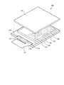
図1は、本発明の一実施形態に係る表示装置100を示す斜視図である。表示装置100は、絶縁表面を有する基板102の一主面に画素部104、タッチセンサ108が配置されている。画素部104は、複数の画素106が配置される。複数の画素106は、画素部104において、例えば、行方向及び列方向に配列される。タッチセンサ108は、画素部104に重ねて配置される。別言すれば、タッチセンサ108は、複数の画素106と重なるように配置される。タッチセンサ108は、複数の検出電極107がマトリクス状に配置され、それぞれが行方向あるいは列方向に接続される。なお、ここでは画素106およびタッチセンサ108は模式的に表現されており、その大小関係は図1記載の限りではない。
First Embodiment:
FIG. 1 is a perspective view showing a
表示装置100は、映像信号等が入力される第1端子領域112a、タッチセンサ108の信号が入出力される第2端子領域112bを有する。第1端子領域112a及び第2端子領域112bは、絶縁表面を有する基板102の一主面における一端部に配置される。第1端子領域112a及び第2端子領域112bは、絶縁表面を有する基板102の端部に沿って複数の端子電極が配列している。第1端子領域112a及び第2端子領域112bの複数の端子電極は、フレキシブルプリント配線基板114と接続される。駆動回路110は、映像信号を画素106に出力する。駆動回路110は、基板102の一主面、又はフレキシブルプリント配線基板114に付設される。
The
絶縁表面を有する基板102は、ガラス、プラスチック(ポリカーボネート、ポリエチレンテレフタレート、ポリイミド、ポリアクリレート等)等の部材で構成される。基板102の材質がプラスチックである場合、基板の薄板化により表示装置100に可撓性を付与することが可能となる。すなわち、基板102としてプラスチック基板を用いることにより、フレキシブルディスプレイを提供することができる。
The
画素部104及びタッチセンサ108の上には、偏光子を含む偏光板116が設けられていてもよい。例えば、偏光板116は、円偏光性を示す偏光子により構成される。偏光板116は、偏光子を含むフィルム基材により形成される。画素部104に重ねて偏光板116を設けることにより、表示画面の映り込み(鏡面化)を防止することができる。
A
なお、図1では省略されているが、画素106は表示素子及び回路素子を含んで構成される。タッチセンサ108は静電容量式であることが好ましく、タッチセンサ108において、第1検出電極(Tx配線)と第2検出電極(Rx配線)によりセンシング部が構成される。画素部104とタッチセンサ108との間には層間絶縁層が設けられ、電気的に相互に短絡しないように配置される。
Although omitted in FIG. 1, the
図2は、画素部104と、その上に配置されるタッチセンサ108の構成を示す斜視図である。図2に示すように、画素部104は、基板102上に回路素子が設けられる回路素子層122、表示素子が設けられる表示素子層124を含む。表示素子層124の上には、タッチセンサ用の検出電極を含む封止層126が設けられる。封止層126は、観察者側の主面を上としたとき画素領域の上側の面を覆うように設けられる。
FIG. 2 is a perspective view showing the configuration of the
回路素子層122は、層間絶縁層を含む。層間絶縁層は、異なる層に設けられる配線を絶縁する。層間絶縁層は、少なくとも一層の無機層間絶縁層と、少なくとも一層の有機層間絶縁層を含む。無機層間絶縁層は、酸化シリコン、窒化シリコン、酸窒化シリコン、酸化アルミニウム等の無機絶縁材料によって形成される。有機層間絶縁層は、アクリル、ポリイミドなどの有機絶縁材料によって形成される。回路素子層122は、トランジスタ等の能動素子、キャパシタ、抵抗等の受動素子、これらの素子を繋ぐ配線を含み、これらが層間絶縁層に埋設するように設けられる。
The
表示素子層124は、表示素子として、発光素子又は電圧の印加により電気光学効果を発現する電気光学素子等が用いられる。発光素子として有機EL素子が用いられる場合、表示素子層124は、アノード及びカソードとして区別される一対の電極、有機EL材料を含む有機層、隣接する有機EL素子間を分離する絶縁性の隔壁層を含んで構成される。有機EL素子は、回路素子層122のトランジスタと電気的に接続される。
As the
封止層126は、複数の絶縁膜が積層された構造を有する。図2は、封止層126として、第1無機絶縁層128、有機絶縁層130及び第2無機絶縁層132が積層された構造を有する。封止層126は、異なる素材を組み合わせた積層構造により、封止性能を高めている。例えば、第1無機絶縁層128に欠陥が含まれても、有機絶縁層130がその欠陥部分を埋め込み、さらに第2無機絶縁層132を設けることで当該欠陥による封止性能の劣化を補うことのできる構造を有している。このとき第2無機絶縁層132は画素部104の全面と、画素部104の外側の領域の少なくとも一部を覆うように設けられてもよく、第1無機絶縁層128と第2無機絶縁層132は第2無機絶縁層132のさらに外側の領域を覆うように形成されてもよい。また第1無機絶縁層128と第2無機絶縁層132の外周端部は必ずしも一致して無くてもよい。
The
タッチセンサ108のセンシング部を構成する第1検出電極134及び第2検出電極140のうち、第1検出電極134は封止層126に内包され、第2検出電極140は封止層126の上側に配置される。なお、図2には示されていないが、第2検出電極140の上側の面は、オーバーコート層184により被覆されていてもよい。
Of the
第1検出電極134は第1方向に延伸するように配置され、第2検出電極140は第1方向と交差する第2方向に延伸するように配置される。第1方向は任意の方向とすることができるが、例えば、画素の配列に対応して列方向に沿った方向としてもよい。この場合第2方向としては、画素の行方向の配列に沿った方向としてもよい。第1検出電極134と第2検出電極140は、それぞれ複数配置される。本実施形態では、複数の第1検出電極134による一群を第1検出電極パターンとも呼び、複数の第2検出電極140による一群を第2検出電極パターンとも呼ぶ。なお、図2では、第1検出電極134及び第2検出電極140の一部が示されているにすぎず、これらの検出電極は、画素部104の略全体に亘って、複数並んで配置される。
The
このような第1検出電極134と第2検出電極140とは、少なくとも封止層126を構成する第2無機絶縁層132を挟んで配置される。第1検出電極134と第2検出電極140とは、少なくとも第2無機絶縁層132により絶縁されている。すなわち、少なくとも第2無機絶縁層132より下層に第1検出電極134が配置され、少なくとも第2無機絶縁層132より上層に第2検出電極140が配置される。第1検出電極134と第2検出電極140とは、少なくとも第2無機絶縁層132を挟んで配置されることにより絶縁され、両検出電極の間に静電容量が発生する。タッチセンサ108のセンシング部は、第1検出電極134と第2検出電極140との間に生ずる静電容量の変化を検知することで、タッチの有無を判別する。
Such a
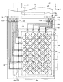
図3は、表示装置100の平面図を示す。図3は、第1検出電極134及び第2検出電極140の配置を模式的に示す。図3は、説明の便宜上、紙面に対して上下方向をY方向、左右方向をX方向として示す。
FIG. 3 shows a plan view of the
図3において、複数の第1検出電極134はY方向に延伸し、複数の第2検出電極140がX方向に延伸している。ここで、複数の第1検出電極134の一群を第1検出電極パターン138とし、複数の第2検出電極140の一群を第2検出電極パターン144とする。
In FIG. 3, the plurality of
なお、第1検出電極134及び第2検出電極140の形状は任意である。第1検出電極134及び第2検出電極140は、長方形(ストライプ)型であってもよいし、図3に示されるように菱(ダイヤモンド)型の電極を連接した形状を有していてもよい。このような長方形(ストライプ)型ないし菱(ダイヤモンド)型を連続して配置した形状の検出電極を採用することにより、タッチセンサ108の検出感度の向上が図られる。
The shapes of the
第1検出電極パターン138及び第2検出電極パターン144は画素部104と重なる領域に配置される。別言すれば、第1検出電極と第2検出電極は、少なくとも画素106の一部(画素に設けられた発光素子の一部分)と重なるように配置される。このように配置されることで、画素部104にアイコン等の画像を表示させつつ、タッチセンサ108によりタッチの有無をセンシングすることができる。
The first
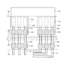
図4は本発明の一実施形態に係る表示装置100の周辺領域の構成を示す平面図である。図4は、図3に示す平面図の一部拡大図である。図3及び図4を参照すると、画素部104は、封止層126で覆われている。第1検出電極134は、画素部104の外側において、封止層126に設けられる開口部133において第1配線136aと電気的に接続される。第1配線136aは、第2端子領域112bに設けられる、タッチパネル用の接続端子である第2端子115aと電気的に接続される。第2端子115aは、フレキシブルプリント配線基板114と接続される第1端子113aと第2配線137aにより電気的に接続される。
FIG. 4 is a plan view showing the configuration of the peripheral region of the
第2検出電極140は、画素部104の外側に設けられる第1配線136bと電気的に接続される。第1配線136bは、第2端子領域112bの第2端子115bと電気的に接続される。第1配線136b、第1端子113b及び第2端子115bの構成は、第1配線136a、第1端子113a及び第2端子115aの構成と、それぞれ同様である。
The
図2において、画素部104の外側にある周辺領域118に含まれる駆動回路110bは、図示しないが、複数のトランジスタが設けられる。例えば、複数のトランジスタは、nチャネル型トランジスタ、又はpチャネル型トランジスタ、あるいはその両方を含む。このようなトランジスタによって駆動回路が形成される。
In FIG. 2, the
基板102には、画素部104を囲む開口領域120が設けられている。この開口領域120においては、基板102と第2無機絶縁層との間にある有機材料が除去されている。別言すれば、基板102上の層間絶縁層は、少なくとも一層の無機層間絶縁層及び有機層間絶縁層を含み、無機層間絶縁層と有機層間絶縁層が積層される積層領域と、有機層間絶縁層が除去され無機層間絶縁層が残存する開口領域とを有する。開口領域120の詳細は、後述される画素部104の断面構造によって説明される。第1配線136a、136bは、画素部104から、この開口領域120の上を通って基板102の周縁部に引き出されてもよい。
The
図4に示すように、本発明の一実施形態に係る表示装置100では、開口領域120は、平面視において開口部133と第2端子115a、115bとの間を横断する位置に配置される。この実施形態では、画素部104から、第1配線136a、136bが、この開口領域120の上を通って基板102の周縁部まで引き出されている。
As shown in FIG. 4, in the
図3に示すように、第2端子領域112bは、フレキシブルプリント配線基板114を介してタッチセンサ制御部109と接続される。すなわち、第1検出電極134及び第2検出電極140により得られる検知信号は、第1配線136a、136b、並びに第2配線137a、137bにより第2端子領域112bに伝達され、フレキシブルプリント配線基板114を介してタッチセンサ制御部109に出力される。
As shown in FIG. 3, the second
本発明の一実施形態に係る表示装置100は、タッチセンサ108のセンシング部を構成する第1検出電極パターン138と第2検出電極パターン144とが、基板102上に設けられる。このような構成により、別部品として提供されるタッチセンサを外付けする必要がないので、表示装置100の薄型化を図ることができる。図2で示すように、第1検出電極134は封止層126に埋設されるように設けられ、第2検出電極140は封止層126の上に接するように設けられる。この構成により、第1検出電極134と第2検出電極140との間で静電容量を形成するための誘電体層が、封止層126の一部で代替されるため、表示装置100の薄型化が図られる。
In the
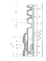
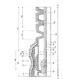
図5は、本発明の一実施形態に係る表示装置100の断面構造を示す。図5は、画素部104及び画素部104の外側に位置する周辺領域118の断面構造を模式的に示す。この断面構造は、図3で示すX1−X2線に沿った構造に対応する。
FIG. 5 shows a cross-sectional structure of the
図5で示すように、基板102上に画素部104と周辺領域118とが設けられる。周辺領域118は第1配線136aを含む配線部と、第1端子113a及び第2端子115aを含む第2端子領域112bとを含む。また、周辺領域118には、画素部104及び有機絶縁層130が形成された領域の外周に沿って形成される開口領域120を含む。画素部104は、トランジスタ146、有機EL素子150、第1容量素子152、第2容量素子154を含む。これらの素子を含む画素106の詳細を図6に示す。
As shown in FIG. 5, a
図6で示すように、有機EL素子150はトランジスタ146と電気的に接続される。トランジスタ146はゲートに印加される映像信号によってソース・ドレイン間を流れる電流が制御され、この電流によって有機EL素子150の発光輝度が制御される。第1容量素子152はトランジスタ146のゲート電圧を保持し、第2容量素子154は画素電極170の電位が不用意に変動するのを防ぐために設けられる。なお、第2容量素子154は必須の構成ではなく省略可能である。
As shown in FIG. 6, the
図6で示すように、基板102の第1面には下地絶縁層156が設けられる。トランジスタ146は、下地絶縁層156上に設けられる。トランジスタ146は、半導体層158、ゲート絶縁層160、ゲート電極162が積層された構造を含む。半導体層158は、非晶質又は多結晶のシリコン、若しくは酸化物半導体等で形成される。ソース・ドレイン配線164は、第1絶縁層166を介して、ゲート電極162の上層に設けられる。ソース・ドレイン配線164の上層には平坦化層としての第2絶縁層168が設けられる。
As shown in FIG. 6, a
第1絶縁層166、第2絶縁層168は層間絶縁層である。第1絶縁層166は、無機層間絶縁層の一種であり、酸化シリコン、窒化シリコン、酸窒化シリコン、酸化アルミニウム等の無機絶縁材料で形成される。第2絶縁層168は、有機層間絶縁層の一種であり、ポリイミド、アクリル等の有機絶縁材料で形成される。層間絶縁層は、基板102側から第1絶縁層166、第2絶縁層168の順に積層される。有機絶縁材料で形成される第2絶縁層168を第1絶縁層166の上層に設けることで、トランジスタ146等に起因する凹凸を埋め込み、表面が平坦化される。
The first insulating
第2絶縁層168の上面に有機EL素子150が設けられる。有機EL素子150は、トランジスタ146と電気的に接続される画素電極170と、有機層172及び対向電極174とが積層された構造を有する。有機EL素子150は2端子素子であり、画素電極170と対向電極174との間の電圧を制御することで発光が制御される。第2絶縁層168上には、画素電極170の周縁部を覆い内側領域を露出するように、隔壁層176が設けられる。対向電極174は、有機層172の上面に設けられる。有機層172は、画素電極170と重なる領域から隔壁層176の上面部にかけて設けられる。隔壁層176は、画素電極170の周縁部を覆うと共に、画素電極170の端部で滑らかな段差を形成するために、有機樹脂材料で形成される。有機樹脂材料としては、アクリルやポリイミドなどが用いられる。
The
有機層172は、有機EL材料を含む単層又は複数の層で形成される。有機層172は、低分子系又は高分子系の有機材料を用いて形成される。低分子系の有機材料を用いる場合、有機層172は有機EL材料を含む発光層に加え、当該発光層を挟むように正孔注入層や電子注入層、さらに正孔輸送層や電子輸送層等含んで構成される。例えば、有機層172は、発光層をホール注入層と電子注入層とで挟んだ構造とすることができる。また、有機層172は、ホール注入層と電子注入層に加え、ホール輸送層、電子輸送層、ホールブロック層、電子ブロック層などを適宜付加されてもよい。
The
なお、本実施形態において、有機EL素子150は、有機層172で発光した光を対向電極174側に放射する、いわゆるトップエミッション型の構造を有する。そのため、画素電極170は光反射性を有することが好ましい。画素電極170は、アルミニウム(Al)、銀(Ag)等の光反射性の金属材料によって形成されることの他、正孔注入性に優れるITO(Indium Tin Oxide:酸化インジウム・スズ)やIZO(Indium Zinc Oxide:酸化インジウム・亜鉛)による透明導電層と、光反射性の金属層とが積層された構造を有する。
In the present embodiment, the
対向電極174は、有機層172で発光した光を透過させるため、透光性を有しかつ導電性を有するITOやIZO等の透明導電膜で形成されている。対向電極174と有機層172との界面には、キャリア注入性を高めるために、リチウム等のアルカリ金属又はマグネシウム等のアルカリ土類金属を含む層が設けられていてもよい。
The
第1容量素子152は、ゲート絶縁層160を誘電体膜として用い、半導体層158と第1容量電極178とが重畳する領域に形成される。また、第2容量素子154は、画素電極170と第2容量電極180との間に設けられる第3絶縁層182を誘電体膜として用い、画素電極170と画素電極に重畳して設けられる第2容量電極180とにより形成される。第3絶縁層182は、窒化シリコン等の無機絶縁材料で形成される。
The
有機EL素子150の上層には封止層126が設けられる。封止層126は、有機EL素子150に水分等が浸入することを防ぐために設けられる。封止層126は、有機EL素子150の側から、第1無機絶縁層128、有機絶縁層130及び第2無機絶縁層132が積層された構造を有する。第1無機絶縁層128及び第2無機絶縁層132は、窒化シリコン、窒酸化シリコン、酸化アルミニウム等の無機絶縁材料により形成される。第1無機絶縁層128及び第2無機絶縁層132は、これらの無機絶縁材料の被膜を、スパッタリング法、プラズマCVD法等により形成される。第1無機絶縁層128及び第2無機絶縁層132は、0.1μm〜10μm、好ましくは0.5μm〜5μmの厚さで形成される。
A
有機絶縁層130は、アクリル樹脂、ポリイミド樹脂、エポキシ樹脂等により形成されることが好ましい。有機絶縁層130は、1μm〜20μm、好ましくは2μm〜10μmの厚さで設けられる。有機絶縁層130は、スピンコーティング等の塗布法や、有機材料ソースを用いた蒸着法によって成膜される。有機絶縁層130は、画素部104を覆うと共に、端部が第1無機絶縁層128及び第2無機絶縁層132で封止されるように、画素部104を含む所定の領域内に形成されることが好ましい。例えば、図5に示すように、有機絶縁層130の端部(輪郭部)は、画素部104と開口領域120との間に設けられることが好ましい。このため、有機絶縁層130は、塗布法により基板102へ全面成膜した後、エッチングにより外周領域を除去するか、被蒸着面を開口するマスクを用いた蒸着法(マスク蒸着)、インクジェット印刷、フレキソ印刷、グラビア印刷により、予め所定のパターンに形成することが好ましい。さらに、図5に示すように、封止層126の上層には、画素部104及び周辺領域118のうちの配線部及び第2端子115aを覆い、第1端子113aを露出するオーバーコート層184が設けられてもよい。
The organic insulating
なお、図5では省略されているが、封止層126の上面には、図1で示すように偏光板116が設けられる。偏光板116には、偏光子の他、カラーフィルタ層、遮光層が適宜含まれていてもよい。
Although omitted in FIG. 5, a
タッチセンサ108の第1検出電極134は、第1無機絶縁層128と有機絶縁層130との間に設けられ、第2検出電極140は、第2無機絶縁層132の上に設けられる。第1検出電極134及び第2検出電極140は、有機EL素子150から出射される光を透過するために透明導電膜で形成された透明電極であってもよい。透明導電膜の一種であるITOやIZOの被膜はスパッタリング法で作製される。
The
第1検出電極134及び第2検出電極140は、ITO、IZO等の酸化物導電材料の他、金属ナノワイヤーを用いて印刷法で透明電極として作製されてもよいし、金属膜を用いたメッシュ金属配線であってもよい。この場合、メッシュ金属配線とは、第1検出電極134及び第2検出電極140を構成する導電層部分が、有機EL素子150と重ならない領域のみに形成されることにより得られる形状を意味している。例えば、第1検出電極134及び第2検出電極140のうち少なくとも1方の電極は、チタン(Ti)層、アルミニウム(Al)層及びチタン(Ti)層を含む積層構造を有するメッシュ配線で形成されてもよい。
The
好ましくは、第1検出電極134がチタン層、アルミニウム層及びチタン層を含む積層構造を有するメッシュ配線で形成され、第2検出電極140がITOやIZOなどの透明導電膜で形成されたダイヤモンド電極であってもよい。この場合、第1検出電極134が、第2無機絶縁層132上の第1配線136a、136bと電気的に接続するための開口部133を形成するとともに、第1端子領域112a及び第2端子領域112b上の無機絶縁層を除去して端子を露出するプロセスにおいて、第1検出電極134の最表面にチタンが位置するので、プロセス尤度が大きくなる。
Preferably, the
より好ましくは、第1検出電極134及び第2検出電極140が、いずれもチタン層、アルミニウム層及びチタン層を含む積層構造を有するメッシュ配線で形成されてもよい。この場合も、第1検出電極134が、第2無機絶縁層132上の第1配線136a、136bと電気的に接続するための開口部133を形成するとともに、第1端子領域112a及び第2端子領域112b上の無機絶縁層を除去して端子を露出するプロセスにおいて、第1検出電極134の最表面にチタンが位置するので、プロセス尤度が大きくなる。さらに、第1検出電極134又は第2検出電極140のいずれを用いて画素部104から周辺領域118まで引き回すための配線を形成しても、ITOやIZOなどの透明導電膜で引き回し配線を形成する場合と異なり、エッチングによる膜厚減少を考慮する必要がないため、厚膜化が不要となり低抵抗を実現することができる。
More preferably, the
本実施形態においては、第1検出電極134の上層に有機絶縁層130が形成されるので、第1検出電極134を形成する透明導電膜等を成膜した後に異物が付着していても、当該異物を有機絶縁層130で被覆することができる。それにより、有機絶縁層130上に形成される第2検出電極140と、第1検出電極134とが短絡するのを防ぐことができる。さらに、有機絶縁層130の上層には第2無機絶縁層132が設けられるので、封止層126としての機能を維持することができる。
In the present embodiment, since the organic insulating
図3に示すように、開口領域120は、画素部104と駆動回路110bとの間に設けられる。開口領域120は、第2絶縁層168を貫通する開口部を含む。開口領域120は、画素部104の少なくとも一辺に沿って設けられる。好ましくは、開口領域120は、画素部104を囲むように設けられる。図5に示すように、第2絶縁層168は、開口領域120によって画素部104側と駆動回路110b側とに分断されている。別言すれば、開口領域120の開口部において、有機材料によって形成される第2絶縁層168が除去されている。
As shown in FIG. 3, the
図5に示すように、封止層126を構成する有機絶縁層130は、開口領域120と画素部104との間に端部が配置される。第1無機絶縁層128及び第2無機絶縁層132は、有機絶縁層130の端部の外側まで延設される。これにより有機絶縁層130の外側領域では、第1無機絶縁層128と第2無機絶縁層132とが接する構造が形成される。別言すれば、有機絶縁層130は、第1無機絶縁層128と第2無機絶縁層132により挟み込まれ、端部が露出しない構造を有している。この構造により、有機絶縁層130の端部から水分等が浸入することを防止することができる。
As shown in FIG. 5, the organic insulating
このように、周辺領域118において有機絶縁材料で形成される第2絶縁層168を開口領域120によって分断し、開口領域120の側面及び底面を被覆するように無機材料層が配設されることで、封止構造が形成される。有機絶縁材料で形成される第2絶縁層168を、無機材料の層により挟み込むことで、基板102の端部から画素部104に水分が浸入することを防ぐことができる。第2絶縁層168を分離する開口領域120は水分遮断領域として機能させることができ、その構造を「水分遮断構造」ということができる。
In this way, the second insulating
次に、表示装置100の製造方法を説明する。図7は本発明の一実施形態に係る表示装置100の製造方法を説明するフローチャートであり、封止層126及び第1検出電極134、及び第2検出電極140を作製する工程を示す。
Next, a method of manufacturing the
まず、絶縁表面を有する基板102の一主面に有機EL素子150を形成した後、第1無機絶縁層128を作製する(図7、S10)。図12は、この段階における表示装置100の断面図を示す。図12に示すように、基板102上に、トランジスタ146、有機EL素子150、第1容量素子152、第2容量素子154、第2端子115、開口領域120が形成された後、これらを覆うように第1無機絶縁層128が形成される。第1無機絶縁層128は、プラズマCVD(Chemical Vapor Deposition)法のような気相成長法により作製される。第1無機絶縁層128は、窒化シリコン膜、窒酸化シリコン膜などで作製される。
First, the
第1無機絶縁層128を作製後、第1検出電極134を作製する(図7、S12及びS14)。図13に示すように、第1検出電極134は、第1無機絶縁層128の上に形成される。第1検出電極134を作製するために、まず、スパッタリング法によりIZOなどの透明導電膜が、第1無機絶縁層134の略全面に成膜される(図7、S12)。その後、フォトリソグラフィ工程により所定の形状にパターニングされることで、第1検出電極134が形成される(図7、S14)。
After producing the first inorganic insulating
次に、印刷法などにより有機絶縁層130を形成する(図7、S16)。図14に示すように、有機絶縁層130は、画素部104を覆い、開口領域120からはみ出さないように形成される。有機絶縁層130は、インクジェット法などにより作製される。有機絶縁層130は、アクリル樹脂、ポリイミド樹脂、エポキシ樹脂などの所定の有機樹脂材料の前駆体を含む組成物を、インクヘッドから吐出させ、画素部104の上に塗布した後、焼成することにより作製される。有機絶縁層130は感光性材料を用いて現像工程を経て形成されてもよい。
Next, the organic insulating
そして、第2無機絶縁層132を形成する(図7、S18)。図14に示すように、第2無機絶縁層132は、基板102の略全面に形成される。第2無機絶縁層132は、有機絶縁層130を覆い、有機絶縁層130が設けられない領域では、第1検出電極134を覆い、さらにその外側の領域では第1無機絶縁層128と密接するように形成される。
Then, the second inorganic insulating
以上までの段階で、封止層126が形成される。この段階では、封止層126が第1端子領域112a及び第2端子領域112bを覆ってしまうので、これらの領域を覆う封止層126を除去するために、第1無機絶縁層128及び第2無機絶縁層132をパターニングする工程が行われる(図7、S20)。図15は、第1無機絶縁層132の上に、フォトリソグラフィ工程によりマスクを形成し、第2端子領域112bを露出させた段階を示す。この段階で、第2無機絶縁層132には、第1検出電極134を露出させる開口部133が同時に一括形成される。
At the above steps, the
その後、第1検出電極140を作製する(図7、S22及びS24)。第2検出電極140は、第2無機絶縁層134の上に形成される。第2検出電極140を作製するために、まず、スパッタリング法によりIZOなどの透明導電膜が、第2無機絶縁層132の略全面に成膜される(図7、S22)。その後、フォトリソグラフィ工程により所定の形状にパターニングされることで、図5に示すように、第2検出電極140が形成される(図7、S24)。
Then, the
本実施形態では、第1無機絶縁層及び第2無機絶縁層をエッチングする段階(S20)において、第1無機絶縁層128及び第2無機絶縁層132をエッチングする際に、第1検出電極134を露出させる開口部133を第2無機絶縁層132に形成する。ここで、第1検出電極134を構成する金属と第1無機絶縁層128及び第2無機絶縁層132を構成する無機絶縁膜(窒化シリコン膜)とのエッチングレートに差があるため、開口部133の形成と第2端子領域112bの無機絶縁層除去とを同一のエッチング工程にて一括してパターニングすることができる。これにより、表示装置100の製造工程を低減し、製造コストを削減することができる。
In the present embodiment, in the step (S20) of etching the first inorganic insulating layer and the second inorganic insulating layer, when the first inorganic insulating
本実施形態によれば、第1検出電極134と第2検出電極140との間で静電容量を形成するための誘電体層が、封止層126の一部で代替されるため、表示装置の層数を低減して薄型化を図ることができる。また、第2無機絶縁層132上の開口部133となるコンタクトホールの形成工程と、第2端子領域上の無機絶縁層の除去工程(端子出し)とを一括してパターニングすることができるので、表示装置の層数及び製造工程の低減を同時に実現することができるので、製造コストを削減することができる。また、表示装置の層数が低減されると、発光効率が向上し、製品製造時の歩留まりも向上する。
According to the present embodiment, the dielectric layer for forming the capacitance between the
このような構造は、基板102が有機樹脂材料で形成されるシート状の基板においても適用可能であり、タッチパネルが内蔵されたフレキシブルディスプレイにおいて層数及び製造工程の低減を実現することができる。
Such a structure can also be applied to a sheet-shaped substrate in which the
第2実施形態:
図8は、本実施形態に係る表示装置200の周辺領域の構成を示す平面図であり、図9は、本実施形態に係る表示装置200の構成を示す断面図である。図8及び図9に示す表示装置200は、第1実施形態にかかる表示装置100と異なり、第1検出電極134と第1配線136とを接続する開口部133が、開口領域120の外側に設けられている。本実施形態では、第1配線136は、開口領域120を横断して開口部133まで延長されている。
Second embodiment:
FIG. 8 is a plan view showing the configuration of the peripheral region of the
また、図8及び図9に示す表示装置200は、第1実施形態にかかる表示装置100と異なり、タッチセンサ108の第1検出電極134が、有機絶縁層130と第2無機絶縁層132との間に設けられている。したがって、表示装置200において、タッチセンサ108の第1検出電極134と第2検出電極140とによって構成されるセンシング部は、その間に位置する第2無機絶縁層132によって絶縁されている。
ただし、第1検出電極134と第2検出電極140とは、少なくとも第2無機絶縁層132によって絶縁されていれば足りるため、本実施形態においても表示装置100と同様に第1検出電極134が、第1無機絶縁層128と有機絶縁層130との間に設けられていてもよい。
Further, in the
However, since it is sufficient that the
本実施形態にかかる表示装置200のその他の構成は、第1実施形態にかかる表示装置100と同様であり、同様の作用効果を奏する。さらに、本実施形態にかかる表示装置200は、第2端子領域102bの近傍まで、第1検出電極134が、封止層126を構成する第1無機絶縁層128と第2無機絶縁層132とに挟まれて配設されるので、配線の劣化、腐食がより低減し、タッチセンサの信頼性を向上させることができる。
Other configurations of the
第3実施形態:
図10は、本実施形態に係る表示装置300の周辺領域の構成を示す平面図であり、図11は、本実施形態に係る表示装置300の構成を示す断面図である。図10及び図11に示す表示装置300は、第1実施形態にかかる表示装置100と異なり、開口領域120が、第2端子115a、115bの外側に設けられており、かつ、第1検出電極134と第1配線136とを接続する開口部133が、第2端子115a、115bの内側に設けられている。表示装置300のその他の構成は表示装置100と同様である。
Third Embodiment:
FIG. 10 is a plan view showing the configuration of the peripheral region of the
図10及び図11で示すように、第1配線136は、開口領域120を横断することなく、開口領域120の内側で、開口部133を介して第2端子115a、115bと接続される。このような配線構造により、第1配線136の配線長が短縮され、また第1配線136が開口領域120による段差を乗り越える必要がないので、配線の劣化が防止され、タッチセンサの信頼性を向上させることができる。
As shown in FIGS. 10 and 11, the first wiring 136 is connected to the
本実施形態にかかる表示装置300のその他の構成は、第1実施形態にかかる表示装置100と同様であり、同様の作用効果を奏する。
Other configurations of the
100,200,300・・・表示装置、102・・・基板、104・・・画素部、106・・・画素、107・・・検出電極、108・・・タッチセンサ、109・・・タッチセンサ制御部、110・・・駆動回路、112・・・端子領域、113・・・第1端子、114・・・フレキシブルプリント配線基板、115・・・第2端子、116・・・偏光板、118・・・周辺領域、120・・・開口領域、122・・・回路素子層、124・・・表示素子層、126・・・封止層、128・・・第1無機絶縁層、130・・・有機絶縁層、132・・・第2無機絶縁層、133・・・開口部、134・・・第1検出電極、136・・・第1配線、137・・・第2配線、138・・・第1検出電極パターン、140・・・第2検出電極、144・・・第2検出電極パターン、146・・・トランジスタ、150・・・有機EL素子、152・・・第1容量素子、154・・・第2容量素子、156・・・下地絶縁層、158・・・半導体層、160・・・ゲート絶縁層、162・・・ゲート電極、164・・・ソース・ドレイン配線、166・・・第1絶縁層、168・・・第2絶縁層、170・・・画素電極、172・・・有機層、174・・・対向電極、176・・・隔壁層、178・・・第1容量電極、180・・・第2容量電極、182・・・第3絶縁層、184・・・オーバーコート層 100, 200, 300 ... Display device, 102 ... Board, 104 ... Pixel part, 106 ... Pixel, 107 ... Detection electrode, 108 ... Touch sensor, 109 ... Touch sensor Control unit, 110 ... drive circuit, 112 ... terminal area, 113 ... first terminal, 114 ... flexible printed wiring board, 115 ... second terminal, 116 ... polarizing plate, 118 ... peripheral region, 120 ... opening region, 122 ... circuit element layer, 124 ... display element layer, 126 ... sealing layer, 128 ... first inorganic insulating layer, 130 ... -Organic insulating layer, 132 ... second inorganic insulating layer, 133 ... opening, 134 ... first detection electrode, 136 ... first wiring, 137 ... second wiring, 138 ... 1st detection electrode pattern, 140 ... 2nd detection electrode, 144 ... 2nd detection electrode pattern, 146 ... Transistor, 150 ... Organic EL element, 152 ... 1st capacitance element, 154 ... 2nd capacitance element, 156 ... Underlayer insulating layer, 158 ... Semiconductor layer, 160 ... Gate insulating layer, 162 ... Gate electrode, 164 ... Source / drain wiring, 166 ... First insulating layer, 168 ... second insulating layer, 170 ... pixel electrode, 172 ... organic layer, 174 ... counter electrode, 176 ... partition layer, 178 ... first capacitance Electrode, 180 ... 2nd capacitance electrode, 182 ... 3rd insulating layer, 184 ... Overcoat layer
Claims (9)
前記絶縁表面に配置された複数の画素が配列する画素部と、
前記絶縁表面上で前記画素部の外側の領域に配置される第1端子と、前記第1端子より内側の領域に配置された第2端子と、を含む端子部と、
前記画素部と前記端子部との間に配置される第1配線を含む配線部と、
前記画素部に重ねて配置されたセンシング部と、
前記画素部及び前記配線部を覆う封止部と、を含み、
前記封止部は、
第1無機絶縁層、有機絶縁層、及び第2無機絶縁層を前記基板側からこの順で含み、
前記有機絶縁層は前記画素部と重なる領域に配置され、前記第1無機絶縁層及び前記第2無機絶縁層は前記画素部及び前記配線部と重なる領域に配置され、
前記基板と前記第1無機絶縁層との間に層間絶縁膜を含み、
前記センシング部は、
前記第1無機絶縁層より上層側であって、前記第2無機絶縁層より下層側に配置された第1検出電極と、
前記第2無機絶縁層の上層側に配置された第2検出電極と、を含み、
前記配線部は、
前記第1配線が、前記第2無機絶縁層に設けられた開口部で、前記第1検出電極と電気的に接続され、かつ、前記第2無機絶縁層の外側領域に延伸して、前記第2端子と電気的に接続され、
前記層間絶縁膜は、前記第1端子と前記第2端子との間に、前記層間絶縁膜を貫通する開口領域を有することを特徴とする表示装置。 A substrate with an insulating surface and
A pixel portion in which a plurality of pixels arranged on the insulating surface are arranged, and a pixel portion.
A terminal portion including a first terminal arranged in a region outside the pixel portion on the insulating surface and a second terminal arranged in a region inside the first terminal.
A wiring portion including a first wiring arranged between the pixel portion and the terminal portion,
A sensing unit that is placed on top of the pixel unit and
Includes the pixel portion and the sealing portion that covers the wiring portion.
The sealing portion is
The first inorganic insulating layer, the organic insulating layer, and the second inorganic insulating layer are included in this order from the substrate side.
The organic insulating layer is arranged in a region overlapping the pixel portion, and the first inorganic insulating layer and the second inorganic insulating layer are arranged in a region overlapping the pixel portion and the wiring portion.
An interlayer insulating film is included between the substrate and the first inorganic insulating layer.
The sensing unit
The first detection electrode, which is on the upper layer side of the first inorganic insulating layer and is arranged on the lower layer side of the second inorganic insulating layer,
A second detection electrode arranged on the upper layer side of the second inorganic insulating layer is included.
The wiring part is
The first wiring is electrically connected to the first detection electrode at an opening provided in the second inorganic insulating layer, and extends to the outer region of the second inorganic insulating layer. Electrically connected to 2 terminals,
A display device characterized in that the interlayer insulating film has an opening region penetrating the interlayer insulating film between the first terminal and the second terminal.
前記層間絶縁膜は、前記開口部と前記画素部との間に、前記層間絶縁膜を貫通する開口領域をさらに有する、請求項1から請求項3のいずれか一つに記載の表示装置。 An interlayer insulating film is included between the substrate and the first inorganic insulating layer.
The display device according to any one of claims 1 to 3, wherein the interlayer insulating film further has an opening region penetrating the interlayer insulating film between the opening and the pixel portion.
前記絶縁表面上で前記画素部の外側の領域に第1端子を含む端子部を形成し、
前記絶縁表面上で前記画素部と前記端子部の間に第2端子を形成し、
前記画素部を覆う第1無機絶縁層を形成し、
前記第1無機絶縁層上に、第1方向に延びる第1検出電極層を形成し、
前記第1検出電極層を覆う有機絶縁層を形成し、
前記有機絶縁層を覆う第2無機絶縁層を形成し、
前記基板と前記第1無機絶縁層との間に層間絶縁膜を形成し、
前記第2端子上の前記第1無機絶縁層と前記第2無機絶縁層とを除去するとともに、前記第2無機絶縁層に前記第1検出電極層を露出する開口部を形成し、
前記第1端子と前記第2端子との間に、前記層間絶縁膜を貫通する開口領域を形成し、
前記第2無機絶縁層上に、前記第1方向と交差する方向に延びる第2検出電極層を形成するとともに、前記第2端子に接続し、前記第2無機絶縁層に設けられた開口部で、前記第1検出電極層に接続する第1配線を形成することを特徴とする表示装置の製造方法。 A pixel portion in which a plurality of pixels are arranged is formed on a substrate having an insulating surface, and a pixel portion is formed.
A terminal portion including the first terminal is formed on the insulating surface in a region outside the pixel portion.
A second terminal is formed between the pixel portion and the terminal portion on the insulating surface.
A first inorganic insulating layer covering the pixel portion is formed, and the first inorganic insulating layer is formed.
A first detection electrode layer extending in the first direction is formed on the first inorganic insulating layer, and the first detection electrode layer is formed.
An organic insulating layer covering the first detection electrode layer is formed.
A second inorganic insulating layer covering the organic insulating layer is formed.
An interlayer insulating film is formed between the substrate and the first inorganic insulating layer.
The first inorganic insulating layer and the second inorganic insulating layer on the second terminal are removed, and an opening is formed in the second inorganic insulating layer to expose the first detection electrode layer.
An opening region penetrating the interlayer insulating film is formed between the first terminal and the second terminal.
A second detection electrode layer extending in a direction intersecting the first direction is formed on the second inorganic insulating layer, and is connected to the second terminal at an opening provided in the second inorganic insulating layer. , A method of manufacturing a display device, which comprises forming a first wiring connected to the first detection electrode layer.
Priority Applications (5)
| Application Number | Priority Date | Filing Date | Title |
|---|---|---|---|
| JP2017155333A JP6906397B2 (en) | 2017-08-10 | 2017-08-10 | Display device |
| PCT/JP2018/029905 WO2019031579A1 (en) | 2017-08-10 | 2018-08-09 | Display device |
| CN201880048513.6A CN110959147B (en) | 2017-08-10 | 2018-08-09 | display device |
| US16/773,066 US20200159356A1 (en) | 2017-08-10 | 2020-01-27 | Display device |
| JP2021107983A JP7119180B2 (en) | 2017-08-10 | 2021-06-29 | Display device |
Applications Claiming Priority (1)
| Application Number | Priority Date | Filing Date | Title |
|---|---|---|---|
| JP2017155333A JP6906397B2 (en) | 2017-08-10 | 2017-08-10 | Display device |
Related Child Applications (1)
| Application Number | Title | Priority Date | Filing Date |
|---|---|---|---|
| JP2021107983A Division JP7119180B2 (en) | 2017-08-10 | 2021-06-29 | Display device |
Publications (3)
| Publication Number | Publication Date |
|---|---|
| JP2019036016A JP2019036016A (en) | 2019-03-07 |
| JP2019036016A5 JP2019036016A5 (en) | 2020-09-24 |
| JP6906397B2 true JP6906397B2 (en) | 2021-07-21 |
Family
ID=65272437
Family Applications (2)
| Application Number | Title | Priority Date | Filing Date |
|---|---|---|---|
| JP2017155333A Active JP6906397B2 (en) | 2017-08-10 | 2017-08-10 | Display device |
| JP2021107983A Active JP7119180B2 (en) | 2017-08-10 | 2021-06-29 | Display device |
Family Applications After (1)
| Application Number | Title | Priority Date | Filing Date |
|---|---|---|---|
| JP2021107983A Active JP7119180B2 (en) | 2017-08-10 | 2021-06-29 | Display device |
Country Status (4)
| Country | Link |
|---|---|
| US (1) | US20200159356A1 (en) |
| JP (2) | JP6906397B2 (en) |
| CN (1) | CN110959147B (en) |
| WO (1) | WO2019031579A1 (en) |
Families Citing this family (9)
| Publication number | Priority date | Publication date | Assignee | Title |
|---|---|---|---|---|
| JP7110764B2 (en) * | 2017-10-17 | 2022-08-02 | 株式会社デンソー | heater device |
| KR102819120B1 (en) * | 2019-06-18 | 2025-06-13 | 삼성디스플레이 주식회사 | Display apparatus |
| WO2021081988A1 (en) * | 2019-11-01 | 2021-05-06 | 京东方科技集团股份有限公司 | Display module and display device |
| CN114442832B (en) * | 2020-11-04 | 2024-09-17 | 宸美(厦门)光电有限公司 | Touch panel and method for manufacturing the same |
| KR20220072017A (en) | 2020-11-23 | 2022-06-02 | 삼성디스플레이 주식회사 | Display device and method of manufacturing the same |
| US11675448B2 (en) | 2020-12-11 | 2023-06-13 | Tpk Advanced Solutions Inc. | Touch panel and method for forming the same |
| JPWO2022203086A1 (en) | 2021-03-26 | 2022-09-29 | ||
| JPWO2024033737A1 (en) * | 2022-08-10 | 2024-02-15 | ||
| KR20250031265A (en) * | 2023-08-28 | 2025-03-07 | 엘지디스플레이 주식회사 | Display device and method of manufacturing for the same |
Family Cites Families (19)
| Publication number | Priority date | Publication date | Assignee | Title |
|---|---|---|---|---|
| JP5120528B2 (en) * | 2006-03-29 | 2013-01-16 | カシオ計算機株式会社 | Manufacturing method of display device |
| KR100838082B1 (en) * | 2007-03-16 | 2008-06-16 | 삼성에스디아이 주식회사 | OLED display device and manufacturing method |
| JP2008281615A (en) * | 2007-05-08 | 2008-11-20 | Seiko Epson Corp | Electro-optical device, manufacturing method thereof, and electronic apparatus |
| JP5267845B2 (en) * | 2008-03-05 | 2013-08-21 | カシオ計算機株式会社 | Manufacturing method of display device |
| JP6216167B2 (en) * | 2013-06-26 | 2017-10-18 | 株式会社ジャパンディスプレイ | Terminal connection structure and display device with built-in touch sensor |
| KR20150011231A (en) | 2013-07-22 | 2015-01-30 | 삼성디스플레이 주식회사 | Organic light emitting display apparatus and the manufacturing method thereof |
| JP6253923B2 (en) * | 2013-08-30 | 2017-12-27 | 株式会社ジャパンディスプレイ | Organic electroluminescence device with built-in touch sensor |
| JP6371094B2 (en) * | 2014-03-31 | 2018-08-08 | 株式会社ジャパンディスプレイ | Organic EL display device |
| US10073571B2 (en) * | 2014-05-02 | 2018-09-11 | Semiconductor Energy Laboratory Co., Ltd. | Touch sensor and touch panel including capacitor |
| KR102284754B1 (en) * | 2014-10-27 | 2021-08-03 | 삼성디스플레이 주식회사 | Thin film transistor array substrate and organic light-emitting display including the same |
| JP2016201216A (en) * | 2015-04-08 | 2016-12-01 | 株式会社ジャパンディスプレイ | Display device and manufacturing method of display device |
| US10168844B2 (en) | 2015-06-26 | 2019-01-01 | Samsung Display Co., Ltd. | Flexible display device |
| JP2017068928A (en) * | 2015-09-28 | 2017-04-06 | セイコーエプソン株式会社 | Organic light emitting device and electronic device |
| JP6545083B2 (en) * | 2015-11-09 | 2019-07-17 | 三菱電機株式会社 | Touch screen, touch panel, display device and electronic device |
| KR102528294B1 (en) * | 2015-11-12 | 2023-05-04 | 삼성디스플레이 주식회사 | Organic light emitting display and manufacturing method thereof |
| US9837475B2 (en) * | 2015-12-21 | 2017-12-05 | Japan Display Inc. | Display device |
| JP6636807B2 (en) | 2016-01-15 | 2020-01-29 | 株式会社ジャパンディスプレイ | Organic EL display |
| KR102456154B1 (en) | 2016-01-29 | 2022-10-19 | 삼성디스플레이 주식회사 | Sensor, touch sensor and display device |
| KR102810070B1 (en) | 2016-12-27 | 2025-05-21 | 엘지디스플레이 주식회사 | Display device |
-
2017
- 2017-08-10 JP JP2017155333A patent/JP6906397B2/en active Active
-
2018
- 2018-08-09 WO PCT/JP2018/029905 patent/WO2019031579A1/en not_active Ceased
- 2018-08-09 CN CN201880048513.6A patent/CN110959147B/en active Active
-
2020
- 2020-01-27 US US16/773,066 patent/US20200159356A1/en not_active Abandoned
-
2021
- 2021-06-29 JP JP2021107983A patent/JP7119180B2/en active Active
Also Published As
| Publication number | Publication date |
|---|---|
| US20200159356A1 (en) | 2020-05-21 |
| WO2019031579A1 (en) | 2019-02-14 |
| JP7119180B2 (en) | 2022-08-16 |
| CN110959147B (en) | 2023-11-21 |
| CN110959147A (en) | 2020-04-03 |
| JP2021180007A (en) | 2021-11-18 |
| JP2019036016A (en) | 2019-03-07 |
Similar Documents
| Publication | Publication Date | Title |
|---|---|---|
| JP6906397B2 (en) | Display device | |
| US11985884B2 (en) | Display device | |
| JP6975033B2 (en) | Display device | |
| KR101939479B1 (en) | Display device | |
| US11462597B2 (en) | Organic light-emitting display device having touch sensor | |
| US20240381736A1 (en) | Organic Light Emitting Display Having Touch Sensors and Method of Fabricating the Same, and Display Device | |
| JP7529698B2 (en) | Display substrate and display device | |
| US11903291B2 (en) | Organic light-emitting display device having touch sensor | |
| US10868088B2 (en) | Display device | |
| KR101905315B1 (en) | Display device | |
| US10795472B2 (en) | Display device | |
| KR20190076384A (en) | Organic light emitting display device with touch sensor | |
| US20240251593A1 (en) | Display device | |
| JP6815173B2 (en) | Touch sensor and display device |
Legal Events
| Date | Code | Title | Description |
|---|---|---|---|
| A521 | Request for written amendment filed |
Free format text: JAPANESE INTERMEDIATE CODE: A523 Effective date: 20200729 |
|
| A621 | Written request for application examination |
Free format text: JAPANESE INTERMEDIATE CODE: A621 Effective date: 20200729 |
|
| A131 | Notification of reasons for refusal |
Free format text: JAPANESE INTERMEDIATE CODE: A131 Effective date: 20210302 |
|
| A521 | Request for written amendment filed |
Free format text: JAPANESE INTERMEDIATE CODE: A523 Effective date: 20210427 |
|
| TRDD | Decision of grant or rejection written | ||
| A01 | Written decision to grant a patent or to grant a registration (utility model) |
Free format text: JAPANESE INTERMEDIATE CODE: A01 Effective date: 20210601 |
|
| A61 | First payment of annual fees (during grant procedure) |
Free format text: JAPANESE INTERMEDIATE CODE: A61 Effective date: 20210629 |
|
| R150 | Certificate of patent or registration of utility model |
Ref document number: 6906397 Country of ref document: JP Free format text: JAPANESE INTERMEDIATE CODE: R150 |
|
| R250 | Receipt of annual fees |
Free format text: JAPANESE INTERMEDIATE CODE: R250 |
|
| R250 | Receipt of annual fees |
Free format text: JAPANESE INTERMEDIATE CODE: R250 |
|
| S111 | Request for change of ownership or part of ownership |
Free format text: JAPANESE INTERMEDIATE CODE: R313113 |
|
| R350 | Written notification of registration of transfer |
Free format text: JAPANESE INTERMEDIATE CODE: R350 |