WO2019031579A1 - 表示装置 - Google Patents
表示装置 Download PDFInfo
- Publication number
- WO2019031579A1 WO2019031579A1 PCT/JP2018/029905 JP2018029905W WO2019031579A1 WO 2019031579 A1 WO2019031579 A1 WO 2019031579A1 JP 2018029905 W JP2018029905 W JP 2018029905W WO 2019031579 A1 WO2019031579 A1 WO 2019031579A1
- Authority
- WO
- WIPO (PCT)
- Prior art keywords
- insulating layer
- layer
- detection electrode
- inorganic insulating
- terminal
- Prior art date
Links
Images


Classifications
-
- H—ELECTRICITY
- H10—SEMICONDUCTOR DEVICES; ELECTRIC SOLID-STATE DEVICES NOT OTHERWISE PROVIDED FOR
- H10K—ORGANIC ELECTRIC SOLID-STATE DEVICES
- H10K59/00—Integrated devices, or assemblies of multiple devices, comprising at least one organic light-emitting element covered by group H10K50/00
- H10K59/40—OLEDs integrated with touch screens
-
- G—PHYSICS
- G06—COMPUTING; CALCULATING OR COUNTING
- G06F—ELECTRIC DIGITAL DATA PROCESSING
- G06F3/00—Input arrangements for transferring data to be processed into a form capable of being handled by the computer; Output arrangements for transferring data from processing unit to output unit, e.g. interface arrangements
- G06F3/01—Input arrangements or combined input and output arrangements for interaction between user and computer
- G06F3/03—Arrangements for converting the position or the displacement of a member into a coded form
- G06F3/041—Digitisers, e.g. for touch screens or touch pads, characterised by the transducing means
- G06F3/0412—Digitisers structurally integrated in a display
-
- G—PHYSICS
- G06—COMPUTING; CALCULATING OR COUNTING
- G06F—ELECTRIC DIGITAL DATA PROCESSING
- G06F3/00—Input arrangements for transferring data to be processed into a form capable of being handled by the computer; Output arrangements for transferring data from processing unit to output unit, e.g. interface arrangements
- G06F3/01—Input arrangements or combined input and output arrangements for interaction between user and computer
- G06F3/03—Arrangements for converting the position or the displacement of a member into a coded form
- G06F3/041—Digitisers, e.g. for touch screens or touch pads, characterised by the transducing means
- G06F3/0416—Control or interface arrangements specially adapted for digitisers
- G06F3/04164—Connections between sensors and controllers, e.g. routing lines between electrodes and connection pads
-
- G—PHYSICS
- G06—COMPUTING; CALCULATING OR COUNTING
- G06F—ELECTRIC DIGITAL DATA PROCESSING
- G06F3/00—Input arrangements for transferring data to be processed into a form capable of being handled by the computer; Output arrangements for transferring data from processing unit to output unit, e.g. interface arrangements
- G06F3/01—Input arrangements or combined input and output arrangements for interaction between user and computer
- G06F3/03—Arrangements for converting the position or the displacement of a member into a coded form
- G06F3/041—Digitisers, e.g. for touch screens or touch pads, characterised by the transducing means
- G06F3/044—Digitisers, e.g. for touch screens or touch pads, characterised by the transducing means by capacitive means
- G06F3/0445—Digitisers, e.g. for touch screens or touch pads, characterised by the transducing means by capacitive means using two or more layers of sensing electrodes, e.g. using two layers of electrodes separated by a dielectric layer
-
- G—PHYSICS
- G06—COMPUTING; CALCULATING OR COUNTING
- G06F—ELECTRIC DIGITAL DATA PROCESSING
- G06F3/00—Input arrangements for transferring data to be processed into a form capable of being handled by the computer; Output arrangements for transferring data from processing unit to output unit, e.g. interface arrangements
- G06F3/01—Input arrangements or combined input and output arrangements for interaction between user and computer
- G06F3/03—Arrangements for converting the position or the displacement of a member into a coded form
- G06F3/041—Digitisers, e.g. for touch screens or touch pads, characterised by the transducing means
- G06F3/044—Digitisers, e.g. for touch screens or touch pads, characterised by the transducing means by capacitive means
- G06F3/0446—Digitisers, e.g. for touch screens or touch pads, characterised by the transducing means by capacitive means using a grid-like structure of electrodes in at least two directions, e.g. using row and column electrodes
-
- G—PHYSICS
- G09—EDUCATION; CRYPTOGRAPHY; DISPLAY; ADVERTISING; SEALS
- G09F—DISPLAYING; ADVERTISING; SIGNS; LABELS OR NAME-PLATES; SEALS
- G09F9/00—Indicating arrangements for variable information in which the information is built-up on a support by selection or combination of individual elements
- G09F9/30—Indicating arrangements for variable information in which the information is built-up on a support by selection or combination of individual elements in which the desired character or characters are formed by combining individual elements
-
- H—ELECTRICITY
- H05—ELECTRIC TECHNIQUES NOT OTHERWISE PROVIDED FOR
- H05B—ELECTRIC HEATING; ELECTRIC LIGHT SOURCES NOT OTHERWISE PROVIDED FOR; CIRCUIT ARRANGEMENTS FOR ELECTRIC LIGHT SOURCES, IN GENERAL
- H05B33/00—Electroluminescent light sources
- H05B33/02—Details
- H05B33/04—Sealing arrangements, e.g. against humidity
-
- H—ELECTRICITY
- H05—ELECTRIC TECHNIQUES NOT OTHERWISE PROVIDED FOR
- H05B—ELECTRIC HEATING; ELECTRIC LIGHT SOURCES NOT OTHERWISE PROVIDED FOR; CIRCUIT ARRANGEMENTS FOR ELECTRIC LIGHT SOURCES, IN GENERAL
- H05B33/00—Electroluminescent light sources
- H05B33/02—Details
- H05B33/06—Electrode terminals
-
- H—ELECTRICITY
- H05—ELECTRIC TECHNIQUES NOT OTHERWISE PROVIDED FOR
- H05B—ELECTRIC HEATING; ELECTRIC LIGHT SOURCES NOT OTHERWISE PROVIDED FOR; CIRCUIT ARRANGEMENTS FOR ELECTRIC LIGHT SOURCES, IN GENERAL
- H05B33/00—Electroluminescent light sources
- H05B33/10—Apparatus or processes specially adapted to the manufacture of electroluminescent light sources
-
- H—ELECTRICITY
- H05—ELECTRIC TECHNIQUES NOT OTHERWISE PROVIDED FOR
- H05B—ELECTRIC HEATING; ELECTRIC LIGHT SOURCES NOT OTHERWISE PROVIDED FOR; CIRCUIT ARRANGEMENTS FOR ELECTRIC LIGHT SOURCES, IN GENERAL
- H05B33/00—Electroluminescent light sources
- H05B33/12—Light sources with substantially two-dimensional radiating surfaces
- H05B33/22—Light sources with substantially two-dimensional radiating surfaces characterised by the chemical or physical composition or the arrangement of auxiliary dielectric or reflective layers
-
- H—ELECTRICITY
- H10—SEMICONDUCTOR DEVICES; ELECTRIC SOLID-STATE DEVICES NOT OTHERWISE PROVIDED FOR
- H10K—ORGANIC ELECTRIC SOLID-STATE DEVICES
- H10K50/00—Organic light-emitting devices
- H10K50/80—Constructional details
- H10K50/84—Passivation; Containers; Encapsulations
- H10K50/844—Encapsulations
- H10K50/8445—Encapsulations multilayered coatings having a repetitive structure, e.g. having multiple organic-inorganic bilayers
-
- H—ELECTRICITY
- H10—SEMICONDUCTOR DEVICES; ELECTRIC SOLID-STATE DEVICES NOT OTHERWISE PROVIDED FOR
- H10K—ORGANIC ELECTRIC SOLID-STATE DEVICES
- H10K59/00—Integrated devices, or assemblies of multiple devices, comprising at least one organic light-emitting element covered by group H10K50/00
- H10K59/10—OLED displays
- H10K59/12—Active-matrix OLED [AMOLED] displays
- H10K59/131—Interconnections, e.g. wiring lines or terminals
-
- H—ELECTRICITY
- H10—SEMICONDUCTOR DEVICES; ELECTRIC SOLID-STATE DEVICES NOT OTHERWISE PROVIDED FOR
- H10K—ORGANIC ELECTRIC SOLID-STATE DEVICES
- H10K71/00—Manufacture or treatment specially adapted for the organic devices covered by this subclass
-
- G—PHYSICS
- G06—COMPUTING; CALCULATING OR COUNTING
- G06F—ELECTRIC DIGITAL DATA PROCESSING
- G06F2203/00—Indexing scheme relating to G06F3/00 - G06F3/048
- G06F2203/041—Indexing scheme relating to G06F3/041 - G06F3/045
- G06F2203/04103—Manufacturing, i.e. details related to manufacturing processes specially suited for touch sensitive devices
-
- G—PHYSICS
- G06—COMPUTING; CALCULATING OR COUNTING
- G06F—ELECTRIC DIGITAL DATA PROCESSING
- G06F2203/00—Indexing scheme relating to G06F3/00 - G06F3/048
- G06F2203/041—Indexing scheme relating to G06F3/041 - G06F3/045
- G06F2203/04112—Electrode mesh in capacitive digitiser: electrode for touch sensing is formed of a mesh of very fine, normally metallic, interconnected lines that are almost invisible to see. This provides a quite large but transparent electrode surface, without need for ITO or similar transparent conductive material
Definitions
- One embodiment of the present invention relates to a display device having an input function.
- One embodiment of the invention disclosed herein relates to a wiring structure of a display device in which a touch sensor is incorporated.
- a display panel used for such an electronic device is also called a touch panel (or touch screen).
- a capacitive touch sensor is adopted.
- capacitive touch sensors there is one that detects a change in electrostatic capacitance between a pair of sensor electrodes, which is also called a Tx electrode and an Rx electrode, as an input signal.
- the conventional touch panel has a structure in which a touch sensor panel and a display panel are superimposed.
- the problem is that the thickness of the display increases.
- a structure in which a touch sensor panel and a display panel are superimposed is a factor that hinders flexibility.
- the structure which built in the function of the touch sensor in the display panel is disclosed.
- a display panel using an organic electroluminescent element hereinafter, also referred to as "organic EL element”
- the first detection electrode and the second detection electrode are disposed with an inorganic insulating film provided as a sealing film interposed therebetween.
- an in-cell type in which a touch sensor is provided in a panel is disclosed (see Patent Document 1).
- the wiring connected with a detection electrode will be needed and the number of wiring layers will increase.
- the display panel needs to protect the display element with the sealing layer, so a process of forming a detection electrode and a wiring or a wiring connected to the detection electrode and a terminal electrode It is necessary to provide a connection structure without deteriorating the sealing performance of the sealing layer.
- a substrate having an insulating surface, a pixel portion in which a plurality of pixels arranged on the insulating surface are arrayed, and a region disposed on the insulating surface in an area outside the pixel portion
- a terminal portion including one terminal and a second terminal disposed in a region inside the first terminal, a wiring portion including a first wiring disposed between the pixel portion and the terminal portion, and a pixel portion overlapping
- the sealing portion covering the pixel portion and the wiring portion, and the sealing portion includes the first inorganic insulating layer, the organic insulating layer, and the second inorganic insulating layer in this order from the substrate side.
- the organic insulating layer is disposed in a region overlapping the pixel portion, the first inorganic insulating layer and the second inorganic insulating layer are disposed in a region overlapping the pixel portion and the wiring portion, and the sensing portion is formed of the first inorganic insulating layer
- a first detection electrode disposed on the upper layer side and lower than the second inorganic insulating layer
- a second detection electrode disposed on the upper layer side of the insulating layer, and the first wiring included in the wiring portion is electrically connected to the first detection electrode at an opening provided in the second inorganic insulating layer
- the first wiring extends to the outer region of the second inorganic insulating layer and is electrically connected to the second terminal.
- a pixel portion in which a plurality of pixels are arrayed is formed on a substrate having an insulating surface, and a terminal including a first terminal in an area outside the pixel portion on the insulating surface.
- a first detection electrode layer is formed, an organic insulating layer covering the first detection electrode layer is formed, a second inorganic insulating layer covering the organic insulating layer is formed, and a first inorganic insulating layer and a second on the second terminal are formed.
- a second detection electrode layer which forms an opening for exposing the first detection electrode layer in the second insulating layer while removing the inorganic insulating layer, and extends in a direction intersecting the first direction on the second inorganic insulating layer.
- a first wiring connected to the second terminal, the opening provided in the second inorganic insulating layer Forming a first wiring connected to the first detection electrode are.
- FIG. 4 is a cross-sectional view taken along line X1-X2 of FIG. 3 showing a configuration of a display device according to an embodiment of the present invention. It is a sectional view showing composition of a pixel field of a display concerning one embodiment of the present invention.
- FIG. 6 shows a flowchart illustrating a method of manufacturing a display device according to an embodiment of the present invention. It is a top view which shows the structure of the peripheral region of the display apparatus which concerns on other embodiment of this invention. It is sectional drawing which shows the structure of the display apparatus which concerns on other embodiment of this invention. It is a top view which shows the structure of the peripheral region of the display apparatus based on other embodiment of this invention. It is sectional drawing which shows the structure of the display apparatus which concerns on further another embodiment of this invention.
- FIG. 7 is a cross-sectional view showing the manufacturing process of the display device according to the embodiment of the present invention. FIG. 7 is a cross-sectional view showing the manufacturing process of the display device according to the embodiment of the present invention. FIG. 7 is a cross-sectional view showing the manufacturing process of the display device according to the embodiment of the present invention.
- FIG. 7 is a cross-sectional view showing the manufacturing process of the display device according to the embodiment of the present invention.
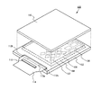
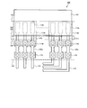
- FIG. 1 is a perspective view showing a display device 100 according to an embodiment of the present invention.
- the pixel portion 104 and the touch sensor 108 are provided on one main surface of a substrate 102 having an insulating surface.
- a plurality of pixels 106 are arranged in the pixel unit 104.
- the plurality of pixels 106 are arranged in, for example, the row direction and the column direction in the pixel unit 104.
- the touch sensor 108 is disposed to overlap the pixel portion 104. In other words, the touch sensor 108 is disposed so as to overlap with the plurality of pixels 106.
- a plurality of detection electrodes 107 are arranged in a matrix, and each is connected in the row direction or the column direction.
- the pixel 106 and the touch sensor 108 are schematically represented, and the magnitude relationship thereof is not limited to that shown in FIG.
- the display device 100 includes a first terminal area 112a to which a video signal or the like is input, and a second terminal area 112b to which signals of the touch sensor 108 are input / output.
- the first terminal region 112 a and the second terminal region 112 b are disposed at one end of one main surface of the substrate 102 having an insulating surface.
- a plurality of terminal electrodes are arranged along the end of the substrate 102 having the insulating surface.
- the plurality of terminal electrodes of the first terminal area 112 a and the second terminal area 112 b are connected to the flexible printed wiring board 114.
- the driver circuit 110 outputs a video signal to the pixel 106.
- the drive circuit 110 is attached to one main surface of the substrate 102 or the flexible printed wiring board 114.
- the substrate 102 having an insulating surface is made of a member such as glass or plastic (polycarbonate, polyethylene terephthalate, polyimide, polyacrylate or the like).
- plastic polycarbonate, polyethylene terephthalate, polyimide, polyacrylate or the like.
- a polarizing plate 116 including a polarizer may be provided on the pixel portion 104 and the touch sensor 108.
- the polarizing plate 116 is configured of a polarizer exhibiting circular polarization.
- the polarizing plate 116 is formed of a film substrate containing a polarizer.
- the pixel 106 includes a display element and a circuit element.
- the touch sensor 108 is preferably an electrostatic capacitance type, and in the touch sensor 108, a sensing unit is configured by the first detection electrode (Tx wiring) and the second detection electrode (Rx wiring).
- An interlayer insulating layer is provided between the pixel portion 104 and the touch sensor 108 and arranged so as not to electrically short each other.
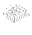
- FIG. 2 is a perspective view showing the configuration of the pixel portion 104 and the touch sensor 108 disposed thereon.
- the pixel portion 104 includes a circuit element layer 122 in which circuit elements are provided on a substrate 102 and a display element layer 124 in which a display element is provided.
- a sealing layer 126 including a detection electrode for the touch sensor is provided on the display element layer 124. The sealing layer 126 is provided so as to cover the upper surface of the pixel region when the main surface on the viewer side is up.
- Circuit element layer 122 includes an interlayer insulating layer.
- the interlayer insulating layer insulates wirings provided in different layers.
- the interlayer insulating layer includes at least one inorganic interlayer insulating layer and at least one organic interlayer insulating layer.
- the inorganic interlayer insulating layer is formed of an inorganic insulating material such as silicon oxide, silicon nitride, silicon oxynitride, or aluminum oxide.
- the organic interlayer insulating layer is formed of an organic insulating material such as acryl or polyimide.
- the circuit element layer 122 includes an active element such as a transistor, a passive element such as a capacitor and a resistor, and a wiring connecting these elements, and is provided so as to be embedded in the interlayer insulating layer.
- the display element layer 124 a light-emitting element or an electro-optical element that exhibits an electro-optical effect by application of a voltage is used as a display element.
- the display element layer 124 includes a pair of electrodes distinguished as an anode and a cathode, an organic layer containing an organic EL material, and an insulating partition layer separating adjacent organic EL elements. It is comprised including.
- the organic EL element is electrically connected to the transistor of the circuit element layer 122.
- the sealing layer 126 has a structure in which a plurality of insulating films are stacked.
- FIG. 2 has a structure in which a first inorganic insulating layer 128, an organic insulating layer 130, and a second inorganic insulating layer 132 are stacked as the sealing layer 126.
- the sealing layer 126 improves sealing performance by a laminated structure in which different materials are combined. For example, even if the first inorganic insulating layer 128 includes a defect, the organic insulating layer 130 burys the defective portion, and the second inorganic insulating layer 132 is further provided to compensate for deterioration in sealing performance due to the defect.
- the second inorganic insulating layer 132 may be provided to cover the entire surface of the pixel portion 104 and at least a part of the region outside the pixel portion 104, and the first inorganic insulating layer 128 and the second inorganic insulating layer 132 may be provided. May be formed to cover a further outside region of the second inorganic insulating layer 132.
- the outer peripheral end portions of the first inorganic insulating layer 128 and the second inorganic insulating layer 132 may not necessarily coincide with each other.
- the first detection electrode 134 and the second detection electrode 140 constituting the sensing unit of the touch sensor 108 the first detection electrode 134 is included in the sealing layer 126, and the second detection electrode 140 is on the upper side of the sealing layer 126. Be placed. Although not shown in FIG. 2, the upper surface of the second detection electrode 140 may be covered with the overcoat layer 184.
- the first detection electrode 134 is disposed to extend in a first direction
- the second detection electrode 140 is disposed to extend in a second direction intersecting the first direction.
- the first direction may be any direction, but may be, for example, a direction along the column direction corresponding to the arrangement of pixels.
- the second direction may be a direction along the arrangement of the pixels in the row direction.
- a plurality of first detection electrodes 134 and a plurality of second detection electrodes 140 are disposed.
- a group of the plurality of first detection electrodes 134 is also referred to as a first detection electrode pattern
- a group of the plurality of second detection electrodes 140 is also referred to as a second detection electrode pattern.
- FIG. 2 only a part of the first detection electrode 134 and the second detection electrode 140 is shown, and a plurality of these detection electrodes are arranged along substantially the entire pixel portion 104. Ru.
- the first detection electrode 134 and the second detection electrode 140 as described above are disposed with at least the second inorganic insulating layer 132 constituting the sealing layer 126 interposed therebetween.
- the first detection electrode 134 and the second detection electrode 140 are insulated by at least a second inorganic insulating layer 132. That is, the first detection electrode 134 is disposed below at least the second inorganic insulating layer 132, and the second detection electrode 140 is disposed above the second inorganic insulating layer 132.
- the first detection electrode 134 and the second detection electrode 140 are insulated by being disposed with at least the second inorganic insulating layer 132 interposed therebetween, and a capacitance is generated between the two detection electrodes.
- the sensing unit of the touch sensor 108 detects a change in capacitance generated between the first detection electrode 134 and the second detection electrode 140 to determine the presence or absence of a touch.
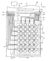
- FIG. 3 shows a plan view of the display device 100.
- FIG. FIG. 3 schematically shows the arrangement of the first detection electrode 134 and the second detection electrode 140.
- FIG. 3 shows the vertical direction as Y direction and the horizontal direction as X direction with respect to the paper surface.
- the plurality of first detection electrodes 134 extend in the Y direction
- the plurality of second detection electrodes 140 extend in the X direction.
- a group of the plurality of first detection electrodes 134 is referred to as a first detection electrode pattern 138
- a group of the plurality of second detection electrodes 140 is referred to as a second detection electrode pattern 144.
- the shapes of the first detection electrode 134 and the second detection electrode 140 are arbitrary.
- the first detection electrode 134 and the second detection electrode 140 may be rectangular (stripe) type, or may have a shape in which diamond (diamond) type electrodes are connected as shown in FIG. .
- the detection sensitivity of the touch sensor 108 can be improved by adopting a detection electrode having a shape in which such rectangular (stripe) type or diamond (diamond) type is continuously arranged.
- the first detection electrode pattern 138 and the second detection electrode pattern 144 are disposed in a region overlapping the pixel unit 104.
- the first detection electrode and the second detection electrode are arranged to overlap at least a part of the pixel 106 (a part of the light emitting element provided in the pixel).
- the touch sensor 108 can sense the presence or absence of a touch while displaying an image such as an icon on the pixel portion 104.
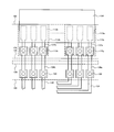
- FIG. 4 is a plan view showing the configuration of the peripheral area of the display device 100 according to an embodiment of the present invention.
- FIG. 4 is a partially enlarged view of the plan view shown in FIG. Referring to FIGS. 3 and 4, the pixel portion 104 is covered with a sealing layer 126.
- the first detection electrode 134 is electrically connected to the first wiring 136 a at the opening 133 provided in the sealing layer 126 outside the pixel portion 104.
- the first wiring 136a is electrically connected to a second terminal 115a provided in the second terminal region 112b, which is a connection terminal for a touch panel.
- the second terminal 115 a is electrically connected by the first terminal 113 a connected to the flexible printed wiring board 114 and the second wiring 137 a.
- the second detection electrode 140 is electrically connected to the first wiring 136 b provided outside the pixel unit 104.
- the first wiring 136 b is electrically connected to the second terminal 115 b of the second terminal region 112 b.
- the configurations of the first wiring 136b, the first terminal 113b, and the second terminal 115b are the same as the configurations of the first wiring 136a, the first terminal 113a, and the second terminal 115a, respectively.
- the drive circuit 110 b included in the peripheral region 118 outside the pixel portion 104 is provided with a plurality of transistors although not shown.
- the plurality of transistors include n-channel transistors, p-channel transistors, or both. Such a transistor forms a drive circuit.
- the substrate 102 is provided with an opening region 120 surrounding the pixel portion 104.
- the interlayer insulating layer on the substrate 102 includes at least one inorganic interlayer insulating layer and an organic interlayer insulating layer, and a laminated region in which the inorganic interlayer insulating layer and the organic interlayer insulating layer are laminated; And an open area where the inorganic interlayer insulating layer remains.
- the details of the opening region 120 are described by the cross-sectional structure of the pixel unit 104 described later.
- the first wires 136 a and 136 b may be drawn from the pixel portion 104 to the periphery of the substrate 102 through the top of the opening region 120.
- the opening region 120 is disposed at a position crossing the opening 133 and the second terminals 115 a and 115 b in a plan view.
- first wirings 136 a and 136 b are drawn from the pixel section 104 to the peripheral edge of the substrate 102 through the top of the opening region 120.
- the second terminal area 112 b is connected to the touch sensor control unit 109 via the flexible printed wiring board 114. That is, detection signals obtained by the first detection electrode 134 and the second detection electrode 140 are transmitted to the second terminal area 112 b by the first wires 136 a and 136 b and the second wires 137 a and 137 b, and the flexible printed wiring board 114 is It is output to the touch sensor control unit 109 via the
- the first detection electrode pattern 138 and the second detection electrode pattern 144 that constitute the sensing unit of the touch sensor 108 are provided on the substrate 102.
- the first detection electrode 134 is provided to be embedded in the sealing layer 126
- the second detection electrode 140 is provided to be in contact with the top of the sealing layer 126.
- the dielectric layer for forming a capacitance between the first detection electrode 134 and the second detection electrode 140 is replaced with a part of the sealing layer 126, so that the display device 100 can be made thin. Can be achieved.
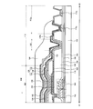
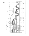
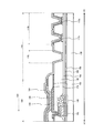
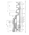
- FIG. 5 shows a cross-sectional structure of a display device 100 according to an embodiment of the present invention.
- FIG. 5 schematically shows a cross-sectional structure of the pixel portion 104 and the peripheral region 118 located outside the pixel portion 104. As shown in FIG. This cross-sectional structure corresponds to the structure along line X1-X2 shown in FIG.
- the pixel portion 104 and the peripheral region 118 are provided on the substrate 102.
- the peripheral region 118 includes a wiring portion including the first wiring 136a, and a second terminal region 112b including the first terminal 113a and the second terminal 115a.
- the peripheral region 118 includes the opening region 120 formed along the outer periphery of the region where the pixel portion 104 and the organic insulating layer 130 are formed.
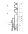
- the pixel portion 104 includes a transistor 146, an organic EL element 150, a first capacitive element 152, and a second capacitive element 154. Details of the pixel 106 including these elements are shown in FIG.
- the organic EL element 150 is electrically connected to the transistor 146.
- the current flowing between the source and the drain is controlled by the video signal applied to the gate of the transistor 146, and the light emission luminance of the organic EL element 150 is controlled by this current.
- the first capacitive element 152 holds the gate voltage of the transistor 146, and the second capacitive element 154 is provided to prevent the potential of the pixel electrode 170 from being inadvertently changed.
- the second capacitive element 154 is not an essential component and can be omitted.
- a base insulating layer 156 is provided on the first surface of the substrate 102.
- the transistor 146 is provided over the base insulating layer 156.
- the transistor 146 includes a structure in which the semiconductor layer 158, the gate insulating layer 160, and the gate electrode 162 are stacked.
- the semiconductor layer 158 is formed using amorphous or polycrystalline silicon, an oxide semiconductor, or the like.
- the source / drain wiring 164 is provided in the upper layer of the gate electrode 162 via the first insulating layer 166.
- a second insulating layer 168 as a planarization layer is provided on the source / drain wiring 164.
- the first insulating layer 166 and the second insulating layer 168 are interlayer insulating layers.
- the first insulating layer 166 is a kind of inorganic interlayer insulating layer, and is formed of an inorganic insulating material such as silicon oxide, silicon nitride, silicon oxynitride, or aluminum oxide.
- the second insulating layer 168 is a type of organic interlayer insulating layer, and is formed of an organic insulating material such as polyimide or acrylic.
- the interlayer insulating layer is stacked in order of the first insulating layer 166 and the second insulating layer 168 from the substrate 102 side.
- the organic EL element 150 is provided on the top surface of the second insulating layer 168.
- the organic EL element 150 has a structure in which a pixel electrode 170 electrically connected to the transistor 146, an organic layer 172, and a counter electrode 174 are stacked.
- the organic EL element 150 is a two-terminal element, and the light emission is controlled by controlling the voltage between the pixel electrode 170 and the counter electrode 174.
- a partition layer 176 is provided on the second insulating layer 168 so as to cover the peripheral portion of the pixel electrode 170 and to expose the inner region.
- the counter electrode 174 is provided on the top surface of the organic layer 172.
- the organic layer 172 is provided from the region overlapping with the pixel electrode 170 to the upper surface portion of the partition layer 176.
- the partition layer 176 is formed of an organic resin material to cover the peripheral portion of the pixel electrode 170 and to form a smooth step at the end portion of the pixel electrode 170. Acrylic or polyimide is used
- the organic layer 172 is formed of a single layer or a plurality of layers containing an organic EL material.
- the organic layer 172 is formed using a low molecular weight or high molecular weight organic material.
- the organic layer 172 is added to the light emitting layer containing the organic EL material, and a hole injecting layer and an electron injecting layer sandwiching the light emitting layer, and a hole transporting layer and an electron transporting layer It comprises.
- the organic layer 172 can have a structure in which the light emitting layer is sandwiched between the hole injection layer and the electron injection layer.
- the organic layer 172 may be appropriately added with a hole transport layer, an electron transport layer, a hole block layer, an electron block layer, and the like.
- the organic EL element 150 has a so-called top emission type structure in which the light emitted from the organic layer 172 is emitted to the counter electrode 174 side. Therefore, the pixel electrode 170 preferably has light reflectivity.
- the pixel electrode 170 is formed of a light reflective metal material such as aluminum (Al) or silver (Ag), or ITO (Indium Tin Oxide: indium tin oxide) or IZO (indium tin oxide) excellent in hole injection property. It has a structure in which a transparent conductive layer of Indium Zinc Oxide: indium oxide / zinc oxide) and a light reflective metal layer are laminated.
- the counter electrode 174 is formed of a transparent conductive film, such as ITO or IZO, which is translucent and has conductivity in order to transmit light emitted from the organic layer 172.
- a layer containing an alkali metal such as lithium or an alkaline earth metal such as magnesium may be provided in order to enhance carrier injection.
- the first capacitor element 152 is formed in a region where the semiconductor layer 158 and the first capacitor electrode 178 overlap, using the gate insulating layer 160 as a dielectric film.
- the second capacitance element 154 uses the third insulating layer 182 provided between the pixel electrode 170 and the second capacitance electrode 180 as a dielectric film, and is provided so as to overlap with the pixel electrode 170 and the pixel electrode.
- the capacitor electrode 180 is formed.
- the third insulating layer 182 is formed of an inorganic insulating material such as silicon nitride.
- a sealing layer 126 is provided in the upper layer of the organic EL element 150.
- the sealing layer 126 is provided to prevent moisture and the like from intruding into the organic EL element 150.
- the sealing layer 126 has a structure in which the first inorganic insulating layer 128, the organic insulating layer 130, and the second inorganic insulating layer 132 are stacked from the organic EL element 150 side.
- the first inorganic insulating layer 128 and the second inorganic insulating layer 132 are formed of an inorganic insulating material such as silicon nitride, silicon oxynitride, or aluminum oxide.
- the first inorganic insulating layer 128 and the second inorganic insulating layer 132 are formed of films of these inorganic insulating materials by a sputtering method, a plasma CVD method, or the like.
- the first inorganic insulating layer 128 and the second inorganic insulating layer 132 are formed to a thickness of 0.1 ⁇ m to 10 ⁇ m, preferably 0.5 ⁇ m to 5 ⁇ m.
- the organic insulating layer 130 is preferably formed of an acrylic resin, a polyimide resin, an epoxy resin, or the like.
- the organic insulating layer 130 is provided with a thickness of 1 ⁇ m to 20 ⁇ m, preferably 2 ⁇ m to 10 ⁇ m.
- the organic insulating layer 130 is formed by a coating method such as spin coating or a vapor deposition method using an organic material source.
- the organic insulating layer 130 is formed in a predetermined region including the pixel portion 104 so as to cover the pixel portion 104 and to seal the end portion with the first inorganic insulating layer 128 and the second inorganic insulating layer 132. Is preferred. For example, as shown in FIG.
- the end (outline portion) of the organic insulating layer 130 is preferably provided between the pixel portion 104 and the opening region 120. Therefore, the organic insulating layer 130 is formed on the entire surface of the substrate 102 by a coating method, and then an outer peripheral region is removed by etching, or an evaporation method (mask evaporation) using a mask that opens a deposition surface, inkjet printing, It is preferable to form in advance a predetermined pattern by flexographic printing or gravure printing. Furthermore, as shown in FIG. 5, an overcoat layer 184 covering the wiring portion and the second terminal 115a in the pixel portion 104 and the peripheral region 118 and exposing the first terminal 113a is provided in the upper layer of the sealing layer 126. It may be provided.
- a polarizing plate 116 is provided on the upper surface of the sealing layer 126 as shown in FIG.
- the polarizing plate 116 may appropriately include a color filter layer and a light shielding layer in addition to the polarizer.
- the first detection electrode 134 of the touch sensor 108 is provided between the first inorganic insulating layer 128 and the organic insulating layer 130, and the second detection electrode 140 is provided on the second inorganic insulating layer 132.
- the first detection electrode 134 and the second detection electrode 140 may be transparent electrodes formed of a transparent conductive film in order to transmit light emitted from the organic EL element 150.
- a film of ITO or IZO, which is a kind of transparent conductive film, is produced by sputtering.
- the first detection electrode 134 and the second detection electrode 140 may be manufactured as a transparent electrode by a printing method using metal nanowires other than oxide conductive materials such as ITO and IZO, or a mesh using a metal film It may be metal wiring.
- the mesh metal wiring means a shape obtained by forming the conductive layer portion constituting the first detection electrode 134 and the second detection electrode 140 only in the region not overlapping the organic EL element 150.
- at least one of the first detection electrode 134 and the second detection electrode 140 is formed of mesh wiring having a laminated structure including a titanium (Ti) layer, an aluminum (Al) layer, and a titanium (Ti) layer. May be
- the first detection electrode 134 is formed of mesh wiring having a laminated structure including a titanium layer, an aluminum layer, and a titanium layer
- the second detection electrode 140 is a diamond electrode formed of a transparent conductive film such as ITO or IZO. It may be.
- the first detection electrode 134 forms an opening 133 for electrically connecting to the first wires 136a and 136b on the second inorganic insulating layer 132, and the first terminal region 112a and the second terminal region
- titanium is positioned on the outermost surface of the first detection electrode 134, so the process likelihood is increased.
- each of the first detection electrode 134 and the second detection electrode 140 may be formed of mesh wiring having a laminated structure including a titanium layer, an aluminum layer, and a titanium layer.
- the first detection electrode 134 forms an opening 133 for electrically connecting to the first wires 136 a and 136 b on the second inorganic insulating layer 132, and the first terminal region 112 a and the second terminal.
- titanium is positioned on the outermost surface of the first detection electrode 134, so the process likelihood is increased.
- the lead wiring is formed of a transparent conductive film such as ITO or IZO. Unlike in the case, it is not necessary to consider the reduction in film thickness due to the etching, so it is not necessary to increase the film thickness, and low resistance can be realized.
- the organic insulating layer 130 is formed on the upper layer of the first detection electrode 134, even if foreign matter adheres after the transparent conductive film or the like for forming the first detection electrode 134 is formed, The foreign matter can be coated with the organic insulating layer 130. Thus, a short circuit between the second detection electrode 140 formed on the organic insulating layer 130 and the first detection electrode 134 can be prevented. Furthermore, since the second inorganic insulating layer 132 is provided on the organic insulating layer 130, the function as the sealing layer 126 can be maintained.
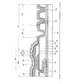
- the opening region 120 is provided between the pixel portion 104 and the drive circuit 110 b.
- the opening region 120 includes an opening penetrating the second insulating layer 168.
- the opening region 120 is provided along at least one side of the pixel portion 104.
- the opening region 120 is provided to surround the pixel portion 104.
- the second insulating layer 168 is divided into the pixel portion 104 side and the drive circuit 110 b side by the opening region 120. In other words, at the opening of the opening region 120, the second insulating layer 168 formed of an organic material is removed.
- the organic insulating layer 130 constituting the sealing layer 126 has an end disposed between the opening region 120 and the pixel portion 104.
- the first inorganic insulating layer 128 and the second inorganic insulating layer 132 are extended to the outside of the end of the organic insulating layer 130.
- a structure in which the first inorganic insulating layer 128 and the second inorganic insulating layer 132 are in contact with each other is formed.
- the organic insulating layer 130 is sandwiched between the first inorganic insulating layer 128 and the second inorganic insulating layer 132, and has a structure in which the end portion is not exposed. This structure can prevent moisture and the like from infiltrating from the end portion of the organic insulating layer 130.
- the second insulating layer 168 formed of the organic insulating material in the peripheral region 118 is divided by the opening region 120, and the inorganic material layer is provided to cover the side surface and the bottom surface of the opening region 120.
- the sealing structure is formed.
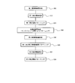
- FIG. 7 is a flowchart for explaining the method of manufacturing the display device 100 according to the embodiment of the present invention, and shows the steps of manufacturing the sealing layer 126, the first detection electrode 134, and the second detection electrode 140.
- the organic EL element 150 is formed on one main surface of the substrate 102 having the insulating surface, and then the first inorganic insulating layer 128 is manufactured (FIG. 7, S10).
- FIG. 12 shows a cross-sectional view of the display device 100 at this stage. As shown in FIG. 12, after the transistor 146, the organic EL element 150, the first capacitance element 152, the second capacitance element 154, the second terminal 115, and the opening region 120 are formed on the substrate 102, they are covered.
- the first inorganic insulating layer 128 is formed.
- the first inorganic insulating layer 128 is manufactured by a vapor deposition method such as plasma CVD (Chemical Vapor Deposition) method.
- the first inorganic insulating layer 128 is formed of a silicon nitride film, a silicon oxynitride film, or the like.
- the first detection electrode 134 is produced (FIG. 7, S12 and S14). As shown in FIG. 13, the first detection electrode 134 is formed on the first inorganic insulating layer 128. In order to produce the first detection electrode 134, first, a transparent conductive film such as IZO is formed on substantially the entire surface of the first inorganic insulating layer 134 by sputtering (FIG. 7, S12). Thereafter, the first detection electrode 134 is formed by patterning into a predetermined shape by a photolithography process (FIG. 7, S14).
- the organic insulating layer 130 is formed by a printing method or the like (FIG. 7, S16). As shown in FIG. 14, the organic insulating layer 130 is formed to cover the pixel portion 104 and not to protrude from the opening region 120.
- the organic insulating layer 130 is manufactured by an inkjet method or the like.
- the organic insulating layer 130 is formed by discharging a composition containing a precursor of a predetermined organic resin material such as an acrylic resin, a polyimide resin, or an epoxy resin from an ink head, applying the composition on the pixel portion 104 and baking it. It is made.
- the organic insulating layer 130 may be formed through a development process using a photosensitive material.
- the second inorganic insulating layer 132 is formed (FIG. 7, S18). As shown in FIG. 14, the second inorganic insulating layer 132 is formed on substantially the entire surface of the substrate 102. The second inorganic insulating layer 132 covers the organic insulating layer 130 and covers the first detection electrode 134 in a region where the organic insulating layer 130 is not provided and is in close contact with the first inorganic insulating layer 128 in a region outside the first detection electrode 134. Is formed.
- the sealing layer 126 is formed by the above steps. At this stage, since the sealing layer 126 covers the first terminal region 112a and the second terminal region 112b, in order to remove the sealing layer 126 covering these regions, the first inorganic insulating layer 128 and the second inorganic insulating layer 128 may be used.
- a step of patterning the inorganic insulating layer 132 is performed (FIG. 7, S20).
- FIG. 15 shows a stage in which a mask is formed on the first inorganic insulating layer 132 by a photolithography process to expose the second terminal region 112b. At this stage, the openings 133 for exposing the first detection electrodes 134 are simultaneously formed in the second inorganic insulating layer 132 simultaneously.
- the first detection electrode 140 is manufactured (FIG. 7, S22 and S24).
- the second detection electrode 140 is formed on the second inorganic insulating layer 134.
- a transparent conductive film such as IZO is formed on substantially the entire surface of the second inorganic insulating layer 132 by sputtering (FIG. 7, S22).
- the second detection electrode 140 is formed as shown in FIG. 5 by being patterned into a predetermined shape by a photolithography process (FIG. 7, S24).
- the first detection electrode 134 is used.
- An opening 133 to be exposed is formed in the second inorganic insulating layer 132.
- the opening 133 And the removal of the inorganic insulating layer of the second terminal region 112b can be collectively patterned in the same etching process. Thereby, the manufacturing process of the display device 100 can be reduced, and the manufacturing cost can be reduced.
- the display device since the dielectric layer for forming a capacitance between the first detection electrode 134 and the second detection electrode 140 is replaced with a part of the sealing layer 126, the display device It is possible to reduce the thickness by reducing the number of layers.
- the step of forming the contact hole to be the opening 133 on the second inorganic insulating layer 132 and the step of removing the inorganic insulating layer on the second terminal region (terminal extraction) can be simultaneously patterned, Since the reduction in the number of layers of the display device and the manufacturing process can be realized simultaneously, the manufacturing cost can be reduced.
- the number of layers of the display device is reduced, the light emission efficiency is improved, and the yield at the time of product manufacture is also improved.
- Such a structure is also applicable to a sheet-like substrate in which the substrate 102 is formed of an organic resin material, and a reduction in the number of layers and manufacturing processes can be realized in a flexible display incorporating a touch panel.
- FIG. 8 is a plan view showing the configuration of the peripheral area of the display device 200 according to the present embodiment
- FIG. 9 is a cross-sectional view showing the configuration of the display device 200 according to the present embodiment.
- the display device 200 shown in FIGS. 8 and 9 is provided with an opening 133 connecting the first detection electrode 134 and the first wiring 136 outside the opening region 120. It is done.
- the first wiring 136 is extended to the opening 133 across the opening area 120.
- the display device 200 shown in FIGS. 8 and 9 has the first detection electrode 134 of the touch sensor 108 that is composed of the organic insulating layer 130 and the second inorganic insulating layer 132. It is provided between. Therefore, in the display device 200, the sensing unit configured by the first detection electrode 134 and the second detection electrode 140 of the touch sensor 108 is insulated by the second inorganic insulating layer 132 located therebetween.
- the first detection electrode 134 and the second detection electrode 140 are insulated by at least the second inorganic insulating layer 132, the first detection electrode 134 is also the same as the display device 100 in the present embodiment, It may be provided between the first inorganic insulating layer 128 and the organic insulating layer 130.
- the other configuration of the display device 200 according to the present embodiment is the same as that of the display device 100 according to the first embodiment, and the same function and effect can be obtained.
- the first detection electrode 134 includes the first inorganic insulating layer 128 and the second inorganic insulating layer 132 constituting the sealing layer 126 up to the vicinity of the second terminal region 102b.
- the sandwiching arrangement can further reduce the deterioration and corrosion of the wiring, and can improve the reliability of the touch sensor.
- FIG. 10 is a plan view showing the configuration of the peripheral area of the display device 300 according to the present embodiment
- FIG. 11 is a cross-sectional view showing the configuration of the display device 300 according to the present embodiment.
- the opening region 120 is provided outside the second terminals 115 a and 115 b, and the first detection electrode 134.
- An opening 133 for connecting the first wiring 136 and the first wiring 136 is provided inside the second terminals 115a and 115b.
- the other configuration of the display device 300 is the same as that of the display device 100.
- the first wiring 136 is connected to the second terminals 115 a and 115 b via the opening 133 inside the opening area 120 without crossing the opening area 120.
- the wiring length of the first wiring 136 is shortened, and the first wiring 136 does not need to get over the step due to the opening region 120, so the deterioration of the wiring is prevented and the reliability of the touch sensor is improved. It can be done.
- the other configuration of the display device 300 according to the present embodiment is the same as that of the display device 100 according to the first embodiment, and the same function and effect can be obtained.
Abstract
絶縁表面に配置された複数の画素が配列する画素部と、絶縁表面上で画素部の外側の領域に配置される第1端子と、第1端子より内側の領域に配置された第2端子とを含む端子部と、画素部と端子部の間に配置される配線部と、画素部に重ねて配置されたセンシング部と、画素部及び配線部を覆う封止部とを含み、封止部は、第1無機絶縁層、有機絶縁層及び第2無機絶縁層を含み、有機絶縁層は画素部と重なり、第1無機絶縁層及び第2無機絶縁層は画素部及び配線部と重なり、センシング部は、第1無機絶縁層と第2無機絶縁層との間に配置された第1検出電極と、第2無機絶縁層の上層側に配置された第2検出電極とを含み、配線部に含まれる第1配線は、第2無機絶縁層に設けられた開口部において第1検出電極と電気的に接続され、第1配線は第2無機絶縁層の外側領域で第2端子と電気的に接続される。
Description
本発明の一実施形態は入力機能を有する表示装置に関する。本明細書で開示される発明の一実施形態は、タッチセンサが組み込まれた表示装置の配線構造に関する。
画面に表示されたアイコン等の画像を触れることで操作が行われる電子機器が普及している。このような電子機器に使用される表示パネルはタッチパネル(若しくはタッチスクリーン)とも呼ばれる。タッチパネルでは、静電容量式のタッチセンサが採用されている。静電容量式のタッチセンサには、Tx電極及びRx電極とも呼ばれる一対のセンサ電極間の静電容量の変化を入力信号として検出しているものがある。
従来のタッチパネルは、タッチセンサパネルと表示パネルとを重ね合わせた構造を有する。しかし、2つのパネルを重ね合わせた構造は、表示装置の厚みが増加することが問題となる。例えば、フレキシブルディスプレイと呼ばれるような、湾曲させたり折り曲げたりする表示装置では、タッチセンサパネルと表示パネルとを重ね合わせた構造が柔軟性を阻害する要因となる。
そこで、タッチセンサの機能を表示パネル内に作り込んだ構造が開示されている。例えば、有機エレクトロルミネセンス素子(以下、「有機EL素子」ともいう。)を用いた表示パネルにおいて、封止膜として設けられる無機絶縁膜を挟んで第1検出電極と第2検出電極とを配置し、タッチセンサをパネル内に設けたインセル型と呼ばれる表示装置が開示されている(特許文献1参照)。
表示パネルにタッチセンサを組み入れようとすると、検出電極と接続する配線が必要となり、配線層の数が増加する。また、配線層の数が増加しない場合でも、表示パネルは、封止層により表示素子を保護する必要があるため、検出電極と配線、または検出電極に接続する配線と端子電極とを形成するプロセスが複雑になり、封止層の封止性能を劣化させずに接続構造を設ける必要がある。
本発明の一実施形態に係る表示装置は、絶縁表面を有する基板と、絶縁表面に配置された複数の画素が配列する画素部と、絶縁表面上で画素部の外側の領域に配置される第1端子と、第1端子より内側の領域に配置された第2端子と、を含む端子部と、画素部と端子部の間に配置される第1配線を含む配線部と、画素部に重ねて配置されたセンシング部と、画素部及び配線部を覆う封止部と、を含み、封止部は、第1無機絶縁層、有機絶縁層、及び第2無機絶縁層を基板側からこの順で含み、有機絶縁層は画素部と重なる領域に配置され、第1無機絶縁層及び第2無機絶縁層は画素部及び配線部と重なる領域に配置され、センシング部は、第1無機絶縁層より上層側であって第2無機絶縁層より下層側に配置された第1検出電極と、第2無機絶縁層の上層側に配置された第2検出電極と、を含み、配線部に含まれる第1配線は、第2無機絶縁層に設けられた開口部において第1検出電極と電気的に接続され、かつ、第1配線は、第2無機絶縁層の外側領域に延伸して、第2端子と電気的に接続される。
本発明の一実施形態による表示装置の製造方法は、絶縁表面を有する基板上に複数の画素を配列した画素部を形成し、絶縁表面上で画素部の外側の領域に第1端子を含む端子部を形成し、絶縁表面上で画素部と端子部の間に第2端子を形成し、画素部を覆う第1無機絶縁層を形成し、第1無機絶縁層上に、第1方向に延びる第1検出電極層を形成し、第1検出電極層を覆う有機絶縁層を形成し、有機絶縁層を覆う第2無機絶縁層を形成し、第2端子上の第1無機絶縁層と第2無機絶縁層とを除去するとともに、第2絶縁層に第1検出電極層を露出する開口部を形成し、第2無機絶縁層上に、第1方向と交差する方向に延びる第2検出電極層を形成するとともに、第2端子に接続する第1配線であって、第2無機絶縁層に設けられた開口部において第1検出電極に接続する第1配線を形成する。
以下、本発明の実施の形態を、図面等を参照しながら説明する。但し、本発明は多くの異なる態様で実施することが可能であり、以下に例示する実施の形態の記載内容に限定して解釈されるものではない。図面は説明をより明確にするため、実際の態様に比べ、各部の幅、厚さ、形状等について模式的に表される場合があるが、あくまで一例であって、本発明の解釈を限定するものではない。また、本明細書と各図において、既出の図に関して前述したものと同様の要素には、同一の符号(又は数字の後にa、bなどを付した符号)を付して、詳細な説明を適宜省略することがある。さらに各要素に対する「第1」、「第2」と付記された文字は、各要素を区別するために用いられる便宜的な標識であり、特段の説明がない限りそれ以上の意味を有さない。
本明細書において、ある部材又は領域が他の部材又は領域の「上に(又は下に)」あるとする場合、特段の限定がない限りこれは他の部材又は領域の直上(又は直下)にある場合のみでなく他の部材又は領域の上方(又は下方)にある場合を含み、すなわち、他の部材又は領域の上方(又は下方)において間に別の構成要素が含まれている場合も含む。なお、以下の説明では、特に断りのない限り、断面視においては、基板の一主面に対して画素領域、タッチセンサが配置される側を「上方」に該当するとして説明する。
第1実施形態:
図1は、本発明の一実施形態に係る表示装置100を示す斜視図である。表示装置100は、絶縁表面を有する基板102の一主面に画素部104、タッチセンサ108が配置されている。画素部104は、複数の画素106が配置される。複数の画素106は、画素部104において、例えば、行方向及び列方向に配列される。タッチセンサ108は、画素部104に重ねて配置される。別言すれば、タッチセンサ108は、複数の画素106と重なるように配置される。タッチセンサ108は、複数の検出電極107がマトリクス状に配置され、それぞれが行方向あるいは列方向に接続される。なお、ここでは画素106およびタッチセンサ108は模式的に表現されており、その大小関係は図1記載の限りではない。
図1は、本発明の一実施形態に係る表示装置100を示す斜視図である。表示装置100は、絶縁表面を有する基板102の一主面に画素部104、タッチセンサ108が配置されている。画素部104は、複数の画素106が配置される。複数の画素106は、画素部104において、例えば、行方向及び列方向に配列される。タッチセンサ108は、画素部104に重ねて配置される。別言すれば、タッチセンサ108は、複数の画素106と重なるように配置される。タッチセンサ108は、複数の検出電極107がマトリクス状に配置され、それぞれが行方向あるいは列方向に接続される。なお、ここでは画素106およびタッチセンサ108は模式的に表現されており、その大小関係は図1記載の限りではない。
表示装置100は、映像信号等が入力される第1端子領域112a、タッチセンサ108の信号が入出力される第2端子領域112bを有する。第1端子領域112a及び第2端子領域112bは、絶縁表面を有する基板102の一主面における一端部に配置される。第1端子領域112a及び第2端子領域112bは、絶縁表面を有する基板102の端部に沿って複数の端子電極が配列している。第1端子領域112a及び第2端子領域112bの複数の端子電極は、フレキシブルプリント配線基板114と接続される。駆動回路110は、映像信号を画素106に出力する。駆動回路110は、基板102の一主面、又はフレキシブルプリント配線基板114に付設される。
絶縁表面を有する基板102は、ガラス、プラスチック(ポリカーボネート、ポリエチレンテレフタレート、ポリイミド、ポリアクリレート等)等の部材で構成される。基板102の材質がプラスチックである場合、基板の薄板化により表示装置100に可撓性を付与することが可能となる。すなわち、基板102としてプラスチック基板を用いることにより、フレキシブルディスプレイを提供することができる。
画素部104及びタッチセンサ108の上には、偏光子を含む偏光板116が設けられていてもよい。例えば、偏光板116は、円偏光性を示す偏光子により構成される。偏光板116は、偏光子を含むフィルム基材により形成される。画素部104に重ねて偏光板116を設けることにより、表示画面の映り込み(鏡面化)を防止することができる。
なお、図1では省略されているが、画素106は表示素子及び回路素子を含んで構成される。タッチセンサ108は静電容量式であることが好ましく、タッチセンサ108において、第1検出電極(Tx配線)と第2検出電極(Rx配線)によりセンシング部が構成される。画素部104とタッチセンサ108との間には層間絶縁層が設けられ、電気的に相互に短絡しないように配置される。
図2は、画素部104と、その上に配置されるタッチセンサ108の構成を示す斜視図である。図2に示すように、画素部104は、基板102上に回路素子が設けられる回路素子層122、表示素子が設けられる表示素子層124を含む。表示素子層124の上には、タッチセンサ用の検出電極を含む封止層126が設けられる。封止層126は、観察者側の主面を上としたとき画素領域の上側の面を覆うように設けられる。
回路素子層122は、層間絶縁層を含む。層間絶縁層は、異なる層に設けられる配線を絶縁する。層間絶縁層は、少なくとも一層の無機層間絶縁層と、少なくとも一層の有機層間絶縁層を含む。無機層間絶縁層は、酸化シリコン、窒化シリコン、酸窒化シリコン、酸化アルミニウム等の無機絶縁材料によって形成される。有機層間絶縁層は、アクリル、ポリイミドなどの有機絶縁材料によって形成される。回路素子層122は、トランジスタ等の能動素子、キャパシタ、抵抗等の受動素子、これらの素子を繋ぐ配線を含み、これらが層間絶縁層に埋設するように設けられる。
表示素子層124は、表示素子として、発光素子又は電圧の印加により電気光学効果を発現する電気光学素子等が用いられる。発光素子として有機EL素子が用いられる場合、表示素子層124は、アノード及びカソードとして区別される一対の電極、有機EL材料を含む有機層、隣接する有機EL素子間を分離する絶縁性の隔壁層を含んで構成される。有機EL素子は、回路素子層122のトランジスタと電気的に接続される。
封止層126は、複数の絶縁膜が積層された構造を有する。図2は、封止層126として、第1無機絶縁層128、有機絶縁層130及び第2無機絶縁層132が積層された構造を有する。封止層126は、異なる素材を組み合わせた積層構造により、封止性能を高めている。例えば、第1無機絶縁層128に欠陥が含まれても、有機絶縁層130がその欠陥部分を埋め込み、さらに第2無機絶縁層132を設けることで当該欠陥による封止性能の劣化を補うことのできる構造を有している。このとき第2無機絶縁層132は画素部104の全面と、画素部104の外側の領域の少なくとも一部を覆うように設けられてもよく、第1無機絶縁層128と第2無機絶縁層132は第2無機絶縁層132のさらに外側の領域を覆うように形成されてもよい。また第1無機絶縁層128と第2無機絶縁層132の外周端部は必ずしも一致して無くてもよい。
タッチセンサ108のセンシング部を構成する第1検出電極134及び第2検出電極140のうち、第1検出電極134は封止層126に内包され、第2検出電極140は封止層126の上側に配置される。なお、図2には示されていないが、第2検出電極140の上側の面は、オーバーコート層184により被覆されていてもよい。
第1検出電極134は第1方向に延伸するように配置され、第2検出電極140は第1方向と交差する第2方向に延伸するように配置される。第1方向は任意の方向とすることができるが、例えば、画素の配列に対応して列方向に沿った方向としてもよい。この場合第2方向としては、画素の行方向の配列に沿った方向としてもよい。第1検出電極134と第2検出電極140は、それぞれ複数配置される。本実施形態では、複数の第1検出電極134による一群を第1検出電極パターンとも呼び、複数の第2検出電極140による一群を第2検出電極パターンとも呼ぶ。なお、図2では、第1検出電極134及び第2検出電極140の一部が示されているにすぎず、これらの検出電極は、画素部104の略全体に亘って、複数並んで配置される。
このような第1検出電極134と第2検出電極140とは、少なくとも封止層126を構成する第2無機絶縁層132を挟んで配置される。第1検出電極134と第2検出電極140とは、少なくとも第2無機絶縁層132により絶縁されている。すなわち、少なくとも第2無機絶縁層132より下層に第1検出電極134が配置され、少なくとも第2無機絶縁層132より上層に第2検出電極140が配置される。第1検出電極134と第2検出電極140とは、少なくとも第2無機絶縁層132を挟んで配置されることにより絶縁され、両検出電極の間に静電容量が発生する。タッチセンサ108のセンシング部は、第1検出電極134と第2検出電極140との間に生ずる静電容量の変化を検知することで、タッチの有無を判別する。
図3は、表示装置100の平面図を示す。図3は、第1検出電極134及び第2検出電極140の配置を模式的に示す。図3は、説明の便宜上、紙面に対して上下方向をY方向、左右方向をX方向として示す。
図3において、複数の第1検出電極134はY方向に延伸し、複数の第2検出電極140がX方向に延伸している。ここで、複数の第1検出電極134の一群を第1検出電極パターン138とし、複数の第2検出電極140の一群を第2検出電極パターン144とする。
なお、第1検出電極134及び第2検出電極140の形状は任意である。第1検出電極134及び第2検出電極140は、長方形(ストライプ)型であってもよいし、図3に示されるように菱(ダイヤモンド)型の電極を連接した形状を有していてもよい。このような長方形(ストライプ)型ないし菱(ダイヤモンド)型を連続して配置した形状の検出電極を採用することにより、タッチセンサ108の検出感度の向上が図られる。
第1検出電極パターン138及び第2検出電極パターン144は画素部104と重なる領域に配置される。別言すれば、第1検出電極と第2検出電極は、少なくとも画素106の一部(画素に設けられた発光素子の一部分)と重なるように配置される。このように配置されることで、画素部104にアイコン等の画像を表示させつつ、タッチセンサ108によりタッチの有無をセンシングすることができる。
図4は本発明の一実施形態に係る表示装置100の周辺領域の構成を示す平面図である。図4は、図3に示す平面図の一部拡大図である。図3及び図4を参照すると、画素部104は、封止層126で覆われている。第1検出電極134は、画素部104の外側において、封止層126に設けられる開口部133において第1配線136aと電気的に接続される。第1配線136aは、第2端子領域112bに設けられる、タッチパネル用の接続端子である第2端子115aと電気的に接続される。第2端子115aは、フレキシブルプリント配線基板114と接続される第1端子113aと第2配線137aにより電気的に接続される。
第2検出電極140は、画素部104の外側に設けられる第1配線136bと電気的に接続される。第1配線136bは、第2端子領域112bの第2端子115bと電気的に接続される。第1配線136b、第1端子113b及び第2端子115bの構成は、第1配線136a、第1端子113a及び第2端子115aの構成と、それぞれ同様である。
図2において、画素部104の外側にある周辺領域118に含まれる駆動回路110bは、図示しないが、複数のトランジスタが設けられる。例えば、複数のトランジスタは、nチャネル型トランジスタ、又はpチャネル型トランジスタ、あるいはその両方を含む。このようなトランジスタによって駆動回路が形成される。
基板102には、画素部104を囲む開口領域120が設けられている。この開口領域120においては、基板102と第2無機絶縁層との間にある有機材料が除去されている。別言すれば、基板102上の層間絶縁層は、少なくとも一層の無機層間絶縁層及び有機層間絶縁層を含み、無機層間絶縁層と有機層間絶縁層が積層される積層領域と、有機層間絶縁層が除去され無機層間絶縁層が残存する開口領域とを有する。開口領域120の詳細は、後述される画素部104の断面構造によって説明される。第1配線136a、136bは、画素部104から、この開口領域120の上を通って基板102の周縁部に引き出されてもよい。
図4に示すように、本発明の一実施形態に係る表示装置100では、開口領域120は、平面視において開口部133と第2端子115a、115bとの間を横断する位置に配置される。この実施形態では、画素部104から、第1配線136a、136bが、この開口領域120の上を通って基板102の周縁部まで引き出されている。
図3に示すように、第2端子領域112bは、フレキシブルプリント配線基板114を介してタッチセンサ制御部109と接続される。すなわち、第1検出電極134及び第2検出電極140により得られる検知信号は、第1配線136a、136b、並びに第2配線137a、137bにより第2端子領域112bに伝達され、フレキシブルプリント配線基板114を介してタッチセンサ制御部109に出力される。
本発明の一実施形態に係る表示装置100は、タッチセンサ108のセンシング部を構成する第1検出電極パターン138と第2検出電極パターン144とが、基板102上に設けられる。このような構成により、別部品として提供されるタッチセンサを外付けする必要がないので、表示装置100の薄型化を図ることができる。図2で示すように、第1検出電極134は封止層126に埋設されるように設けられ、第2検出電極140は封止層126の上に接するように設けられる。この構成により、第1検出電極134と第2検出電極140との間で静電容量を形成するための誘電体層が、封止層126の一部で代替されるため、表示装置100の薄型化が図られる。
図5は、本発明の一実施形態に係る表示装置100の断面構造を示す。図5は、画素部104及び画素部104の外側に位置する周辺領域118の断面構造を模式的に示す。この断面構造は、図3で示すX1-X2線に沿った構造に対応する。
図5で示すように、基板102上に画素部104と周辺領域118とが設けられる。周辺領域118は第1配線136aを含む配線部と、第1端子113a及び第2端子115aを含む第2端子領域112bとを含む。また、周辺領域118には、画素部104及び有機絶縁層130が形成された領域の外周に沿って形成される開口領域120を含む。画素部104は、トランジスタ146、有機EL素子150、第1容量素子152、第2容量素子154を含む。これらの素子を含む画素106の詳細を図6に示す。
図6で示すように、有機EL素子150はトランジスタ146と電気的に接続される。トランジスタ146はゲートに印加される映像信号によってソース・ドレイン間を流れる電流が制御され、この電流によって有機EL素子150の発光輝度が制御される。第1容量素子152はトランジスタ146のゲート電圧を保持し、第2容量素子154は画素電極170の電位が不用意に変動するのを防ぐために設けられる。なお、第2容量素子154は必須の構成ではなく省略可能である。
図6で示すように、基板102の第1面には下地絶縁層156が設けられる。トランジスタ146は、下地絶縁層156上に設けられる。トランジスタ146は、半導体層158、ゲート絶縁層160、ゲート電極162が積層された構造を含む。半導体層158は、非晶質又は多結晶のシリコン、若しくは酸化物半導体等で形成される。ソース・ドレイン配線164は、第1絶縁層166を介して、ゲート電極162の上層に設けられる。ソース・ドレイン配線164の上層には平坦化層としての第2絶縁層168が設けられる。
第1絶縁層166、第2絶縁層168は層間絶縁層である。第1絶縁層166は、無機層間絶縁層の一種であり、酸化シリコン、窒化シリコン、酸窒化シリコン、酸化アルミニウム等の無機絶縁材料で形成される。第2絶縁層168は、有機層間絶縁層の一種であり、ポリイミド、アクリル等の有機絶縁材料で形成される。層間絶縁層は、基板102側から第1絶縁層166、第2絶縁層168の順に積層される。有機絶縁材料で形成される第2絶縁層168を第1絶縁層166の上層に設けることで、トランジスタ146等に起因する凹凸を埋め込み、表面が平坦化される。
第2絶縁層168の上面に有機EL素子150が設けられる。有機EL素子150は、トランジスタ146と電気的に接続される画素電極170と、有機層172及び対向電極174とが積層された構造を有する。有機EL素子150は2端子素子であり、画素電極170と対向電極174との間の電圧を制御することで発光が制御される。第2絶縁層168上には、画素電極170の周縁部を覆い内側領域を露出するように、隔壁層176が設けられる。対向電極174は、有機層172の上面に設けられる。有機層172は、画素電極170と重なる領域から隔壁層176の上面部にかけて設けられる。隔壁層176は、画素電極170の周縁部を覆うと共に、画素電極170の端部で滑らかな段差を形成するために、有機樹脂材料で形成される。有機樹脂材料としては、アクリルやポリイミドなどが用いられる。
有機層172は、有機EL材料を含む単層又は複数の層で形成される。有機層172は、低分子系又は高分子系の有機材料を用いて形成される。低分子系の有機材料を用いる場合、有機層172は有機EL材料を含む発光層に加え、当該発光層を挟むように正孔注入層や電子注入層、さらに正孔輸送層や電子輸送層等含んで構成される。例えば、有機層172は、発光層をホール注入層と電子注入層とで挟んだ構造とすることができる。また、有機層172は、ホール注入層と電子注入層に加え、ホール輸送層、電子輸送層、ホールブロック層、電子ブロック層などを適宜付加されてもよい。
なお、本実施形態において、有機EL素子150は、有機層172で発光した光を対向電極174側に放射する、いわゆるトップエミッション型の構造を有する。そのため、画素電極170は光反射性を有することが好ましい。画素電極170は、アルミニウム(Al)、銀(Ag)等の光反射性の金属材料によって形成されることの他、正孔注入性に優れるITO(Indium Tin Oxide:酸化インジウム・スズ)やIZO(Indium Zinc Oxide:酸化インジウム・亜鉛)による透明導電層と、光反射性の金属層とが積層された構造を有する。
対向電極174は、有機層172で発光した光を透過させるため、透光性を有しかつ導電性を有するITOやIZO等の透明導電膜で形成されている。対向電極174と有機層172との界面には、キャリア注入性を高めるために、リチウム等のアルカリ金属又はマグネシウム等のアルカリ土類金属を含む層が設けられていてもよい。
第1容量素子152は、ゲート絶縁層160を誘電体膜として用い、半導体層158と第1容量電極178とが重畳する領域に形成される。また、第2容量素子154は、画素電極170と第2容量電極180との間に設けられる第3絶縁層182を誘電体膜として用い、画素電極170と画素電極に重畳して設けられる第2容量電極180とにより形成される。第3絶縁層182は、窒化シリコン等の無機絶縁材料で形成される。
有機EL素子150の上層には封止層126が設けられる。封止層126は、有機EL素子150に水分等が浸入することを防ぐために設けられる。封止層126は、有機EL素子150の側から、第1無機絶縁層128、有機絶縁層130及び第2無機絶縁層132が積層された構造を有する。第1無機絶縁層128及び第2無機絶縁層132は、窒化シリコン、窒酸化シリコン、酸化アルミニウム等の無機絶縁材料により形成される。第1無機絶縁層128及び第2無機絶縁層132は、これらの無機絶縁材料の被膜を、スパッタリング法、プラズマCVD法等により形成される。第1無機絶縁層128及び第2無機絶縁層132は、0.1μm~10μm、好ましくは0.5μm~5μmの厚さで形成される。
有機絶縁層130は、アクリル樹脂、ポリイミド樹脂、エポキシ樹脂等により形成されることが好ましい。有機絶縁層130は、1μm~20μm、好ましくは2μm~10μmの厚さで設けられる。有機絶縁層130は、スピンコーティング等の塗布法や、有機材料ソースを用いた蒸着法によって成膜される。有機絶縁層130は、画素部104を覆うと共に、端部が第1無機絶縁層128及び第2無機絶縁層132で封止されるように、画素部104を含む所定の領域内に形成されることが好ましい。例えば、図5に示すように、有機絶縁層130の端部(輪郭部)は、画素部104と開口領域120との間に設けられることが好ましい。このため、有機絶縁層130は、塗布法により基板102へ全面成膜した後、エッチングにより外周領域を除去するか、被蒸着面を開口するマスクを用いた蒸着法(マスク蒸着)、インクジェット印刷、フレキソ印刷、グラビア印刷により、予め所定のパターンに形成することが好ましい。さらに、図5に示すように、封止層126の上層には、画素部104及び周辺領域118のうちの配線部及び第2端子115aを覆い、第1端子113aを露出するオーバーコート層184が設けられてもよい。
なお、図5では省略されているが、封止層126の上面には、図1で示すように偏光板116が設けられる。偏光板116には、偏光子の他、カラーフィルタ層、遮光層が適宜含まれていてもよい。
タッチセンサ108の第1検出電極134は、第1無機絶縁層128と有機絶縁層130との間に設けられ、第2検出電極140は、第2無機絶縁層132の上に設けられる。第1検出電極134及び第2検出電極140は、有機EL素子150から出射される光を透過するために透明導電膜で形成された透明電極であってもよい。透明導電膜の一種であるITOやIZOの被膜はスパッタリング法で作製される。
第1検出電極134及び第2検出電極140は、ITO、IZO等の酸化物導電材料の他、金属ナノワイヤーを用いて印刷法で透明電極として作製されてもよいし、金属膜を用いたメッシュ金属配線であってもよい。この場合、メッシュ金属配線とは、第1検出電極134及び第2検出電極140を構成する導電層部分が、有機EL素子150と重ならない領域のみに形成されることにより得られる形状を意味している。例えば、第1検出電極134及び第2検出電極140のうち少なくとも1方の電極は、チタン(Ti)層、アルミニウム(Al)層及びチタン(Ti)層を含む積層構造を有するメッシュ配線で形成されてもよい。
好ましくは、第1検出電極134がチタン層、アルミニウム層及びチタン層を含む積層構造を有するメッシュ配線で形成され、第2検出電極140がITOやIZOなどの透明導電膜で形成されたダイヤモンド電極であってもよい。この場合、第1検出電極134が、第2無機絶縁層132上の第1配線136a、136bと電気的に接続するための開口部133を形成するとともに、第1端子領域112a及び第2端子領域112b上の無機絶縁層を除去して端子を露出するプロセスにおいて、第1検出電極134の最表面にチタンが位置するので、プロセス尤度が大きくなる。
より好ましくは、第1検出電極134及び第2検出電極140が、いずれもチタン層、アルミニウム層及びチタン層を含む積層構造を有するメッシュ配線で形成されてもよい。この場合も、第1検出電極134が、第2無機絶縁層132上の第1配線136a、136bと電気的に接続するための開口部133を形成するとともに、第1端子領域112a及び第2端子領域112b上の無機絶縁層を除去して端子を露出するプロセスにおいて、第1検出電極134の最表面にチタンが位置するので、プロセス尤度が大きくなる。さらに、第1検出電極134又は第2検出電極140のいずれを用いて画素部104から周辺領域118まで引き回すための配線を形成しても、ITOやIZOなどの透明導電膜で引き回し配線を形成する場合と異なり、エッチングによる膜厚減少を考慮する必要がないため、厚膜化が不要となり低抵抗を実現することができる。
本実施形態においては、第1検出電極134の上層に有機絶縁層130が形成されるので、第1検出電極134を形成する透明導電膜等を成膜した後に異物が付着していても、当該異物を有機絶縁層130で被覆することができる。それにより、有機絶縁層130上に形成される第2検出電極140と、第1検出電極134とが短絡するのを防ぐことができる。さらに、有機絶縁層130の上層には第2無機絶縁層132が設けられるので、封止層126としての機能を維持することができる。
図3に示すように、開口領域120は、画素部104と駆動回路110bとの間に設けられる。開口領域120は、第2絶縁層168を貫通する開口部を含む。開口領域120は、画素部104の少なくとも一辺に沿って設けられる。好ましくは、開口領域120は、画素部104を囲むように設けられる。図5に示すように、第2絶縁層168は、開口領域120によって画素部104側と駆動回路110b側とに分断されている。別言すれば、開口領域120の開口部において、有機材料によって形成される第2絶縁層168が除去されている。
図5に示すように、封止層126を構成する有機絶縁層130は、開口領域120と画素部104との間に端部が配置される。第1無機絶縁層128及び第2無機絶縁層132は、有機絶縁層130の端部の外側まで延設される。これにより有機絶縁層130の外側領域では、第1無機絶縁層128と第2無機絶縁層132とが接する構造が形成される。別言すれば、有機絶縁層130は、第1無機絶縁層128と第2無機絶縁層132により挟み込まれ、端部が露出しない構造を有している。この構造により、有機絶縁層130の端部から水分等が浸入することを防止することができる。
このように、周辺領域118において有機絶縁材料で形成される第2絶縁層168を開口領域120によって分断し、開口領域120の側面及び底面を被覆するように無機材料層が配設されることで、封止構造が形成される。有機絶縁材料で形成される第2絶縁層168を、無機材料の層により挟み込むことで、基板102の端部から画素部104に水分が浸入することを防ぐことができる。第2絶縁層168を分離する開口領域120は水分遮断領域として機能させることができ、その構造を「水分遮断構造」ということができる。
次に、表示装置100の製造方法を説明する。図7は本発明の一実施形態に係る表示装置100の製造方法を説明するフローチャートであり、封止層126及び第1検出電極134、及び第2検出電極140を作製する工程を示す。
まず、絶縁表面を有する基板102の一主面に有機EL素子150を形成した後、第1無機絶縁層128を作製する(図7、S10)。図12は、この段階における表示装置100の断面図を示す。図12に示すように、基板102上に、トランジスタ146、有機EL素子150、第1容量素子152、第2容量素子154、第2端子115、開口領域120が形成された後、これらを覆うように第1無機絶縁層128が形成される。第1無機絶縁層128は、プラズマCVD(Chemical Vapor Deposition)法のような気相成長法により作製される。第1無機絶縁層128は、窒化シリコン膜、窒酸化シリコン膜などで作製される。
第1無機絶縁層128を作製後、第1検出電極134を作製する(図7、S12及びS14)。図13に示すように、第1検出電極134は、第1無機絶縁層128の上に形成される。第1検出電極134を作製するために、まず、スパッタリング法によりIZOなどの透明導電膜が、第1無機絶縁層134の略全面に成膜される(図7、S12)。その後、フォトリソグラフィ工程により所定の形状にパターニングされることで、第1検出電極134が形成される(図7、S14)。
次に、印刷法などにより有機絶縁層130を形成する(図7、S16)。図14に示すように、有機絶縁層130は、画素部104を覆い、開口領域120からはみ出さないように形成される。有機絶縁層130は、インクジェット法などにより作製される。有機絶縁層130は、アクリル樹脂、ポリイミド樹脂、エポキシ樹脂などの所定の有機樹脂材料の前駆体を含む組成物を、インクヘッドから吐出させ、画素部104の上に塗布した後、焼成することにより作製される。有機絶縁層130は感光性材料を用いて現像工程を経て形成されてもよい。
そして、第2無機絶縁層132を形成する(図7、S18)。図14に示すように、第2無機絶縁層132は、基板102の略全面に形成される。第2無機絶縁層132は、有機絶縁層130を覆い、有機絶縁層130が設けられない領域では、第1検出電極134を覆い、さらにその外側の領域では第1無機絶縁層128と密接するように形成される。
以上までの段階で、封止層126が形成される。この段階では、封止層126が第1端子領域112a及び第2端子領域112bを覆ってしまうので、これらの領域を覆う封止層126を除去するために、第1無機絶縁層128及び第2無機絶縁層132をパターニングする工程が行われる(図7、S20)。図15は、第1無機絶縁層132の上に、フォトリソグラフィ工程によりマスクを形成し、第2端子領域112bを露出させた段階を示す。この段階で、第2無機絶縁層132には、第1検出電極134を露出させる開口部133が同時に一括形成される。
その後、第1検出電極140を作製する(図7、S22及びS24)。第2検出電極140は、第2無機絶縁層134の上に形成される。第2検出電極140を作製するために、まず、スパッタリング法によりIZOなどの透明導電膜が、第2無機絶縁層132の略全面に成膜される(図7、S22)。その後、フォトリソグラフィ工程により所定の形状にパターニングされることで、図5に示すように、第2検出電極140が形成される(図7、S24)。
本実施形態では、第1無機絶縁層及び第2無機絶縁層をエッチングする段階(S20)において、第1無機絶縁層128及び第2無機絶縁層132をエッチングする際に、第1検出電極134を露出させる開口部133を第2無機絶縁層132に形成する。ここで、第1検出電極134を構成する金属と第1無機絶縁層128及び第2無機絶縁層132を構成する無機絶縁膜(窒化シリコン膜)とのエッチングレートに差があるため、開口部133の形成と第2端子領域112bの無機絶縁層除去とを同一のエッチング工程にて一括してパターニングすることができる。これにより、表示装置100の製造工程を低減し、製造コストを削減することができる。
本実施形態によれば、第1検出電極134と第2検出電極140との間で静電容量を形成するための誘電体層が、封止層126の一部で代替されるため、表示装置の層数を低減して薄型化を図ることができる。また、第2無機絶縁層132上の開口部133となるコンタクトホールの形成工程と、第2端子領域上の無機絶縁層の除去工程(端子出し)とを一括してパターニングすることができるので、表示装置の層数及び製造工程の低減を同時に実現することができるので、製造コストを削減することができる。また、表示装置の層数が低減されると、発光効率が向上し、製品製造時の歩留まりも向上する。
このような構造は、基板102が有機樹脂材料で形成されるシート状の基板においても適用可能であり、タッチパネルが内蔵されたフレキシブルディスプレイにおいて層数及び製造工程の低減を実現することができる。
第2実施形態:
図8は、本実施形態に係る表示装置200の周辺領域の構成を示す平面図であり、図9は、本実施形態に係る表示装置200の構成を示す断面図である。図8及び図9に示す表示装置200は、第1実施形態にかかる表示装置100と異なり、第1検出電極134と第1配線136とを接続する開口部133が、開口領域120の外側に設けられている。本実施形態では、第1配線136は、開口領域120を横断して開口部133まで延長されている。
図8は、本実施形態に係る表示装置200の周辺領域の構成を示す平面図であり、図9は、本実施形態に係る表示装置200の構成を示す断面図である。図8及び図9に示す表示装置200は、第1実施形態にかかる表示装置100と異なり、第1検出電極134と第1配線136とを接続する開口部133が、開口領域120の外側に設けられている。本実施形態では、第1配線136は、開口領域120を横断して開口部133まで延長されている。
また、図8及び図9に示す表示装置200は、第1実施形態にかかる表示装置100と異なり、タッチセンサ108の第1検出電極134が、有機絶縁層130と第2無機絶縁層132との間に設けられている。したがって、表示装置200において、タッチセンサ108の第1検出電極134と第2検出電極140とによって構成されるセンシング部は、その間に位置する第2無機絶縁層132によって絶縁されている。
ただし、第1検出電極134と第2検出電極140とは、少なくとも第2無機絶縁層132によって絶縁されていれば足りるため、本実施形態においても表示装置100と同様に第1検出電極134が、第1無機絶縁層128と有機絶縁層130との間に設けられていてもよい。
ただし、第1検出電極134と第2検出電極140とは、少なくとも第2無機絶縁層132によって絶縁されていれば足りるため、本実施形態においても表示装置100と同様に第1検出電極134が、第1無機絶縁層128と有機絶縁層130との間に設けられていてもよい。
本実施形態にかかる表示装置200のその他の構成は、第1実施形態にかかる表示装置100と同様であり、同様の作用効果を奏する。さらに、本実施形態にかかる表示装置200は、第2端子領域102bの近傍まで、第1検出電極134が、封止層126を構成する第1無機絶縁層128と第2無機絶縁層132とに挟まれて配設されるので、配線の劣化、腐食がより低減し、タッチセンサの信頼性を向上させることができる。
第3実施形態:
図10は、本実施形態に係る表示装置300の周辺領域の構成を示す平面図であり、図11は、本実施形態に係る表示装置300の構成を示す断面図である。図10及び図11に示す表示装置300は、第1実施形態にかかる表示装置100と異なり、開口領域120が、第2端子115a、115bの外側に設けられており、かつ、第1検出電極134と第1配線136とを接続する開口部133が、第2端子115a、115bの内側に設けられている。表示装置300のその他の構成は表示装置100と同様である。
図10は、本実施形態に係る表示装置300の周辺領域の構成を示す平面図であり、図11は、本実施形態に係る表示装置300の構成を示す断面図である。図10及び図11に示す表示装置300は、第1実施形態にかかる表示装置100と異なり、開口領域120が、第2端子115a、115bの外側に設けられており、かつ、第1検出電極134と第1配線136とを接続する開口部133が、第2端子115a、115bの内側に設けられている。表示装置300のその他の構成は表示装置100と同様である。
図10及び図11で示すように、第1配線136は、開口領域120を横断することなく、開口領域120の内側で、開口部133を介して第2端子115a、115bと接続される。このような配線構造により、第1配線136の配線長が短縮され、また第1配線136が開口領域120による段差を乗り越える必要がないので、配線の劣化が防止され、タッチセンサの信頼性を向上させることができる。
本実施形態にかかる表示装置300のその他の構成は、第1実施形態にかかる表示装置100と同様であり、同様の作用効果を奏する。
100,200,300・・・表示装置、102・・・基板、104・・・画素部、106・・・画素、107・・・検出電極、108・・・タッチセンサ、109・・・タッチセンサ制御部、110・・・駆動回路、112・・・端子領域、113・・・第1端子、114・・・フレキシブルプリント配線基板、115・・・第2端子、116・・・偏光板、118・・・周辺領域、120・・・開口領域、122・・・回路素子層、124・・・表示素子層、126・・・封止層、128・・・第1無機絶縁層、130・・・有機絶縁層、132・・・第2無機絶縁層、133・・・開口部、134・・・第1検出電極、136・・・第1配線、137・・・第2配線、138・・・第1検出電極パターン、140・・・第2検出電極、144・・・第2検出電極パターン、146・・・トランジスタ、150・・・有機EL素子、152・・・第1容量素子、154・・・第2容量素子、156・・・下地絶縁層、158・・・半導体層、160・・・ゲート絶縁層、162・・・ゲート電極、164・・・ソース・ドレイン配線、166・・・第1絶縁層、168・・・第2絶縁層、170・・・画素電極、172・・・有機層、174・・・対向電極、176・・・隔壁層、178・・・第1容量電極、180・・・第2容量電極、182・・・第3絶縁層、184・・・オーバーコート層
Claims (10)
- 絶縁表面を有する基板と、
前記絶縁表面に配置された複数の画素が配列する画素部と、
前記絶縁表面上で前記画素部の外側の領域に配置される第1端子と、前記第1端子より内側の領域に配置された第2端子と、を含む端子部と、
前記画素部と前記端子部との間に配置される第1配線を含む配線部と、
前記画素部に重ねて配置されたセンシング部と、
前記画素部及び前記配線部を覆う封止部と、を含み、
前記封止部は、
第1無機絶縁層、有機絶縁層、及び第2無機絶縁層を前記基板側からこの順で含み、
前記有機絶縁層は前記画素部と重なる領域に配置され、前記第1無機絶縁層及び前記第2無機絶縁層は前記画素部及び前記配線部と重なる領域に配置され、
前記センシング部は、
前記第1無機絶縁層より上層側であって、前記第2無機絶縁層より下層側に配置された第1検出電極と、
前記第2無機絶縁層の上層側に配置された第2検出電極と、を含み、
前記配線部に含まれる前記第1配線は、前記第2無機絶縁層に設けられた開口部において前記第1検出電極と電気的に接続され、かつ、前記第1配線は、前記第2無機絶縁層の外側領域に延伸し、前記第2端子と電気的に接続されることを特徴とする表示装置。 - 前記第1検出電極は、前記第1無機絶縁層と前記有機絶縁層との間に配置される、請求項1に記載の表示装置。
- 前記第1検出電極は、前記有機絶縁層と前記第2無機絶縁層との間に配置される、請求項1に記載の表示装置。
- 前記基板と前記第1無機絶縁層との間に層間絶縁膜を含み、
前記層間絶縁膜は、前記第2端子と前記開口部との間に、前記層間絶縁膜を貫通する開口領域を有する、請求項1に記載の表示装置。 - 前記基板と前記第1無機絶縁層との間に層間絶縁膜を含み、
前記層間絶縁膜は、前記開口部と前記画素部との間に、前記層間絶縁膜を貫通する開口領域を有する、請求項1に記載の表示装置。 - 前記基板と前記第1無機絶縁層との間に層間絶縁膜を含み、
前記層間絶縁膜は、前記第1端子と前記第2端子との間に、前記層間絶縁膜を貫通する開口領域を有する、請求項1に記載の表示装置。 - 前記第1検出電極及び前記第2検出電極は、いずれも、チタン層、アルミニウム層及びチタン層を含む積層構造を有するメッシュ配線で形成されることを特徴とする請求項1に記載の表示装置。
- 前記第1検出電極は、チタン層、アルミニウム層及びチタン層を含む積層構造を有するメッシュ配線で形成され、前記第2検出電極は、透明電極からなるダイヤモンド電極であることを特徴とする請求項1に記載の表示装置。
- 前記第1検出電極は、透明電極からなるダイヤモンド電極であり、前記第2検出電極は、チタン層、アルミニウム層及びチタン層を含む積層構造を有するメッシュ配線で形成されることを特徴とする請求項1に記載の表示装置。
- 絶縁表面を有する基板上に複数の画素を配列した画素部を形成し、
前記絶縁表面上で前記画素部の外側の領域に第1端子を含む端子部を形成し、
前記絶縁表面上で前記画素部と前記端子部の間に第2端子を形成し、
前記画素部を覆う第1無機絶縁層を形成し、
前記第1無機絶縁層上に、第1方向に延びる第1検出電極層を形成し、
前記第1検出電極層を覆う有機絶縁層を形成し、
前記有機絶縁層を覆う第2無機絶縁層を形成し、
前記第2端子上の前記第1無機絶縁層と前記第2無機絶縁層とを除去するとともに、前記第2絶縁層に前記第1検出電極層を露出する開口部を形成し、
前記第2無機絶縁層上に、前記第1方向と交差する方向に延びる第2検出電極層を形成するとともに、前記第2端子に接続する第1配線であって、前記第2無機絶縁層に設けられた開口部において前記第1検出電極に接続する第1配線を形成することを特徴とする表示装置の製造方法。
Priority Applications (2)
| Application Number | Priority Date | Filing Date | Title |
|---|---|---|---|
| CN201880048513.6A CN110959147B (zh) | 2017-08-10 | 2018-08-09 | 显示装置 |
| US16/773,066 US20200159356A1 (en) | 2017-08-10 | 2020-01-27 | Display device |
Applications Claiming Priority (2)
| Application Number | Priority Date | Filing Date | Title |
|---|---|---|---|
| JP2017155333A JP6906397B2 (ja) | 2017-08-10 | 2017-08-10 | 表示装置 |
| JP2017-155333 | 2017-08-10 |
Related Child Applications (1)
| Application Number | Title | Priority Date | Filing Date |
|---|---|---|---|
| US16/773,066 Continuation US20200159356A1 (en) | 2017-08-10 | 2020-01-27 | Display device |
Publications (1)
| Publication Number | Publication Date |
|---|---|
| WO2019031579A1 true WO2019031579A1 (ja) | 2019-02-14 |
Family
ID=65272437
Family Applications (1)
| Application Number | Title | Priority Date | Filing Date |
|---|---|---|---|
| PCT/JP2018/029905 WO2019031579A1 (ja) | 2017-08-10 | 2018-08-09 | 表示装置 |
Country Status (4)
| Country | Link |
|---|---|
| US (1) | US20200159356A1 (ja) |
| JP (2) | JP6906397B2 (ja) |
| CN (1) | CN110959147B (ja) |
| WO (1) | WO2019031579A1 (ja) |
Cited By (3)
| Publication number | Priority date | Publication date | Assignee | Title |
|---|---|---|---|---|
| EP3754716A1 (en) * | 2019-06-18 | 2020-12-23 | Samsung Display Co., Ltd. | Display apparatus |
| KR20230164674A (ko) | 2021-03-26 | 2023-12-04 | 린텍 가부시키가이샤 | 적층체 |
| WO2024033737A1 (ja) * | 2022-08-10 | 2024-02-15 | 株式会社半導体エネルギー研究所 | タッチパネル、及びタッチパネルの作製方法 |
Families Citing this family (4)
| Publication number | Priority date | Publication date | Assignee | Title |
|---|---|---|---|---|
| JP7110764B2 (ja) * | 2017-10-17 | 2022-08-02 | 株式会社デンソー | ヒータ装置 |
| JP7428729B2 (ja) | 2019-11-01 | 2024-02-06 | 京東方科技集團股▲ふん▼有限公司 | 表示モジュール及び表示装置 |
| CN114442832A (zh) * | 2020-11-04 | 2022-05-06 | 宸美(厦门)光电有限公司 | 触控面板及其制造方法 |
| US11675448B2 (en) | 2020-12-11 | 2023-06-13 | Tpk Advanced Solutions Inc. | Touch panel and method for forming the same |
Citations (6)
| Publication number | Priority date | Publication date | Assignee | Title |
|---|---|---|---|---|
| JP2008281615A (ja) * | 2007-05-08 | 2008-11-20 | Seiko Epson Corp | 電気光学装置及びその製造方法、電子機器 |
| JP2015007945A (ja) * | 2013-06-26 | 2015-01-15 | 株式会社ジャパンディスプレイ | 端子接続構造及びタッチセンサ内蔵表示装置 |
| JP2015050245A (ja) * | 2013-08-30 | 2015-03-16 | 株式会社ジャパンディスプレイ | タッチセンサ内蔵有機エレクトロルミネッセンス装置 |
| JP2015228210A (ja) * | 2014-05-02 | 2015-12-17 | 株式会社半導体エネルギー研究所 | タッチセンサ、及びタッチパネル |
| JP2017068928A (ja) * | 2015-09-28 | 2017-04-06 | セイコーエプソン株式会社 | 有機発光装置および電子機器 |
| JP2017091135A (ja) * | 2015-11-09 | 2017-05-25 | 三菱電機株式会社 | タッチスクリーン、タッチパネル、表示装置および電子機器 |
Family Cites Families (13)
| Publication number | Priority date | Publication date | Assignee | Title |
|---|---|---|---|---|
| JP5120528B2 (ja) * | 2006-03-29 | 2013-01-16 | カシオ計算機株式会社 | 表示装置の製造方法 |
| KR100838082B1 (ko) * | 2007-03-16 | 2008-06-16 | 삼성에스디아이 주식회사 | 유기발광 표시장치 및 그 제조방법 |
| JP5267845B2 (ja) * | 2008-03-05 | 2013-08-21 | カシオ計算機株式会社 | 表示装置の製造方法 |
| KR20150011231A (ko) * | 2013-07-22 | 2015-01-30 | 삼성디스플레이 주식회사 | 유기 발광 표시 장치 및 이의 제조 방법 |
| JP6371094B2 (ja) * | 2014-03-31 | 2018-08-08 | 株式会社ジャパンディスプレイ | 有機el表示装置 |
| KR102284754B1 (ko) * | 2014-10-27 | 2021-08-03 | 삼성디스플레이 주식회사 | 박막 트랜지스터 어레이 기판, 및 이를 포함하는 유기 발광 표시 장치 |
| JP2016201216A (ja) * | 2015-04-08 | 2016-12-01 | 株式会社ジャパンディスプレイ | 表示装置及び表示装置の製造方法 |
| US10168844B2 (en) * | 2015-06-26 | 2019-01-01 | Samsung Display Co., Ltd. | Flexible display device |
| KR102528294B1 (ko) * | 2015-11-12 | 2023-05-04 | 삼성디스플레이 주식회사 | 유기 발광 표시 장치 및 그 제조 방법 |
| US9837475B2 (en) * | 2015-12-21 | 2017-12-05 | Japan Display Inc. | Display device |
| JP6636807B2 (ja) * | 2016-01-15 | 2020-01-29 | 株式会社ジャパンディスプレイ | 有機el表示装置 |
| KR102456154B1 (ko) * | 2016-01-29 | 2022-10-19 | 삼성디스플레이 주식회사 | 센서, 터치 센서 및 표시 장치 |
| KR20180076006A (ko) * | 2016-12-27 | 2018-07-05 | 엘지디스플레이 주식회사 | 표시 장치 |
-
2017
- 2017-08-10 JP JP2017155333A patent/JP6906397B2/ja active Active
-
2018
- 2018-08-09 CN CN201880048513.6A patent/CN110959147B/zh active Active
- 2018-08-09 WO PCT/JP2018/029905 patent/WO2019031579A1/ja active Application Filing
-
2020
- 2020-01-27 US US16/773,066 patent/US20200159356A1/en not_active Abandoned
-
2021
- 2021-06-29 JP JP2021107983A patent/JP7119180B2/ja active Active
Patent Citations (6)
| Publication number | Priority date | Publication date | Assignee | Title |
|---|---|---|---|---|
| JP2008281615A (ja) * | 2007-05-08 | 2008-11-20 | Seiko Epson Corp | 電気光学装置及びその製造方法、電子機器 |
| JP2015007945A (ja) * | 2013-06-26 | 2015-01-15 | 株式会社ジャパンディスプレイ | 端子接続構造及びタッチセンサ内蔵表示装置 |
| JP2015050245A (ja) * | 2013-08-30 | 2015-03-16 | 株式会社ジャパンディスプレイ | タッチセンサ内蔵有機エレクトロルミネッセンス装置 |
| JP2015228210A (ja) * | 2014-05-02 | 2015-12-17 | 株式会社半導体エネルギー研究所 | タッチセンサ、及びタッチパネル |
| JP2017068928A (ja) * | 2015-09-28 | 2017-04-06 | セイコーエプソン株式会社 | 有機発光装置および電子機器 |
| JP2017091135A (ja) * | 2015-11-09 | 2017-05-25 | 三菱電機株式会社 | タッチスクリーン、タッチパネル、表示装置および電子機器 |
Cited By (5)
| Publication number | Priority date | Publication date | Assignee | Title |
|---|---|---|---|---|
| EP3754716A1 (en) * | 2019-06-18 | 2020-12-23 | Samsung Display Co., Ltd. | Display apparatus |
| US11189668B2 (en) | 2019-06-18 | 2021-11-30 | Samsung Display Co., Ltd. | Display apparatus |
| US11793051B2 (en) | 2019-06-18 | 2023-10-17 | Samsung Display Co., Ltd. | Display apparatus |
| KR20230164674A (ko) | 2021-03-26 | 2023-12-04 | 린텍 가부시키가이샤 | 적층체 |
| WO2024033737A1 (ja) * | 2022-08-10 | 2024-02-15 | 株式会社半導体エネルギー研究所 | タッチパネル、及びタッチパネルの作製方法 |
Also Published As
| Publication number | Publication date |
|---|---|
| JP7119180B2 (ja) | 2022-08-16 |
| JP2021180007A (ja) | 2021-11-18 |
| US20200159356A1 (en) | 2020-05-21 |
| CN110959147B (zh) | 2023-11-21 |
| CN110959147A (zh) | 2020-04-03 |
| JP2019036016A (ja) | 2019-03-07 |
| JP6906397B2 (ja) | 2021-07-21 |
Similar Documents
| Publication | Publication Date | Title |
|---|---|---|
| CN107527931B (zh) | 显示装置 | |
| CN107797689B (zh) | 显示装置 | |
| US11778879B2 (en) | Display device including concave/convex structure in the inorganic insulation layer | |
| JP7119180B2 (ja) | 表示装置 | |
| JP6756538B2 (ja) | 表示装置 | |
| US10678389B2 (en) | Touch sensor and touch display device having a plurality of touch sensor layers | |
| US20180197924A1 (en) | Touch sensor and display device having touch sensor | |
| JP6742822B2 (ja) | 表示装置 | |
| JP6815173B2 (ja) | タッチセンサ及び表示装置 | |
| JP2017220174A (ja) | 表示装置 | |
| WO2019138721A1 (ja) | 表示装置および表示装置の製造方法 | |
| JP2019124776A (ja) | 表示装置および表示装置の製造方法 | |
| JP2018081917A (ja) | タッチセンサ内蔵有機el装置 |
Legal Events
| Date | Code | Title | Description |
|---|---|---|---|
| 121 | Ep: the epo has been informed by wipo that ep was designated in this application |
Ref document number: 18844050 Country of ref document: EP Kind code of ref document: A1 |
|
| NENP | Non-entry into the national phase |
Ref country code: DE |
|
| 122 | Ep: pct application non-entry in european phase |
Ref document number: 18844050 Country of ref document: EP Kind code of ref document: A1 |