JP6890921B2 - Probe card and contact inspection device - Google Patents
Probe card and contact inspection device Download PDFInfo
- Publication number
- JP6890921B2 JP6890921B2 JP2015207263A JP2015207263A JP6890921B2 JP 6890921 B2 JP6890921 B2 JP 6890921B2 JP 2015207263 A JP2015207263 A JP 2015207263A JP 2015207263 A JP2015207263 A JP 2015207263A JP 6890921 B2 JP6890921 B2 JP 6890921B2
- Authority
- JP
- Japan
- Prior art keywords
- probe
- probe card
- guide
- guide portion
- inspected
- Prior art date
- Legal status (The legal status is an assumption and is not a legal conclusion. Google has not performed a legal analysis and makes no representation as to the accuracy of the status listed.)
- Active
Links
Images


Classifications
-
- G—PHYSICS
- G01—MEASURING; TESTING
- G01R—MEASURING ELECTRIC VARIABLES; MEASURING MAGNETIC VARIABLES
- G01R1/00—Details of instruments or arrangements of the types included in groups G01R5/00 - G01R13/00 and G01R31/00
- G01R1/02—General constructional details
- G01R1/06—Measuring leads; Measuring probes
- G01R1/067—Measuring probes
- G01R1/073—Multiple probes
- G01R1/07307—Multiple probes with individual probe elements, e.g. needles, cantilever beams or bump contacts, fixed in relation to each other, e.g. bed of nails fixture or probe card
- G01R1/07314—Multiple probes with individual probe elements, e.g. needles, cantilever beams or bump contacts, fixed in relation to each other, e.g. bed of nails fixture or probe card the body of the probe being perpendicular to test object, e.g. bed of nails or probe with bump contacts on a rigid support
-
- G—PHYSICS
- G01—MEASURING; TESTING
- G01R—MEASURING ELECTRIC VARIABLES; MEASURING MAGNETIC VARIABLES
- G01R1/00—Details of instruments or arrangements of the types included in groups G01R5/00 - G01R13/00 and G01R31/00
- G01R1/02—General constructional details
- G01R1/06—Measuring leads; Measuring probes
- G01R1/067—Measuring probes
- G01R1/06705—Apparatus for holding or moving single probes
-
- G—PHYSICS
- G01—MEASURING; TESTING
- G01R—MEASURING ELECTRIC VARIABLES; MEASURING MAGNETIC VARIABLES
- G01R1/00—Details of instruments or arrangements of the types included in groups G01R5/00 - G01R13/00 and G01R31/00
- G01R1/02—General constructional details
- G01R1/06—Measuring leads; Measuring probes
- G01R1/067—Measuring probes
- G01R1/06711—Probe needles; Cantilever beams; "Bump" contacts; Replaceable probe pins
- G01R1/06716—Elastic
-
- G—PHYSICS
- G01—MEASURING; TESTING
- G01R—MEASURING ELECTRIC VARIABLES; MEASURING MAGNETIC VARIABLES
- G01R1/00—Details of instruments or arrangements of the types included in groups G01R5/00 - G01R13/00 and G01R31/00
- G01R1/02—General constructional details
- G01R1/06—Measuring leads; Measuring probes
- G01R1/067—Measuring probes
- G01R1/06711—Probe needles; Cantilever beams; "Bump" contacts; Replaceable probe pins
- G01R1/06733—Geometry aspects
-
- G—PHYSICS
- G01—MEASURING; TESTING
- G01R—MEASURING ELECTRIC VARIABLES; MEASURING MAGNETIC VARIABLES
- G01R1/00—Details of instruments or arrangements of the types included in groups G01R5/00 - G01R13/00 and G01R31/00
- G01R1/02—General constructional details
- G01R1/06—Measuring leads; Measuring probes
- G01R1/067—Measuring probes
- G01R1/073—Multiple probes
- G01R1/07307—Multiple probes with individual probe elements, e.g. needles, cantilever beams or bump contacts, fixed in relation to each other, e.g. bed of nails fixture or probe card
- G01R1/07314—Multiple probes with individual probe elements, e.g. needles, cantilever beams or bump contacts, fixed in relation to each other, e.g. bed of nails fixture or probe card the body of the probe being perpendicular to test object, e.g. bed of nails or probe with bump contacts on a rigid support
- G01R1/07328—Multiple probes with individual probe elements, e.g. needles, cantilever beams or bump contacts, fixed in relation to each other, e.g. bed of nails fixture or probe card the body of the probe being perpendicular to test object, e.g. bed of nails or probe with bump contacts on a rigid support for testing printed circuit boards
-
- G—PHYSICS
- G01—MEASURING; TESTING
- G01R—MEASURING ELECTRIC VARIABLES; MEASURING MAGNETIC VARIABLES
- G01R1/00—Details of instruments or arrangements of the types included in groups G01R5/00 - G01R13/00 and G01R31/00
- G01R1/02—General constructional details
- G01R1/06—Measuring leads; Measuring probes
- G01R1/067—Measuring probes
- G01R1/073—Multiple probes
- G01R1/07307—Multiple probes with individual probe elements, e.g. needles, cantilever beams or bump contacts, fixed in relation to each other, e.g. bed of nails fixture or probe card
- G01R1/07364—Multiple probes with individual probe elements, e.g. needles, cantilever beams or bump contacts, fixed in relation to each other, e.g. bed of nails fixture or probe card with provisions for altering position, number or connection of probe tips; Adapting to differences in pitch
- G01R1/07371—Multiple probes with individual probe elements, e.g. needles, cantilever beams or bump contacts, fixed in relation to each other, e.g. bed of nails fixture or probe card with provisions for altering position, number or connection of probe tips; Adapting to differences in pitch using an intermediate card or back card with apertures through which the probes pass
-
- G—PHYSICS
- G01—MEASURING; TESTING
- G01R—MEASURING ELECTRIC VARIABLES; MEASURING MAGNETIC VARIABLES
- G01R31/00—Arrangements for testing electric properties; Arrangements for locating electric faults; Arrangements for electrical testing characterised by what is being tested not provided for elsewhere
- G01R31/28—Testing of electronic circuits, e.g. by signal tracer
- G01R31/2851—Testing of integrated circuits [IC]
- G01R31/2886—Features relating to contacting the IC under test, e.g. probe heads; chucks
-
- G—PHYSICS
- G01—MEASURING; TESTING
- G01R—MEASURING ELECTRIC VARIABLES; MEASURING MAGNETIC VARIABLES
- G01R1/00—Details of instruments or arrangements of the types included in groups G01R5/00 - G01R13/00 and G01R31/00
- G01R1/02—General constructional details
- G01R1/06—Measuring leads; Measuring probes
- G01R1/067—Measuring probes
- G01R1/06711—Probe needles; Cantilever beams; "Bump" contacts; Replaceable probe pins
- G01R1/06716—Elastic
- G01R1/06722—Spring-loaded
-
- G—PHYSICS
- G01—MEASURING; TESTING
- G01R—MEASURING ELECTRIC VARIABLES; MEASURING MAGNETIC VARIABLES
- G01R1/00—Details of instruments or arrangements of the types included in groups G01R5/00 - G01R13/00 and G01R31/00
- G01R1/02—General constructional details
- G01R1/06—Measuring leads; Measuring probes
- G01R1/067—Measuring probes
- G01R1/06777—High voltage probes
-
- G—PHYSICS
- G01—MEASURING; TESTING
- G01R—MEASURING ELECTRIC VARIABLES; MEASURING MAGNETIC VARIABLES
- G01R31/00—Arrangements for testing electric properties; Arrangements for locating electric faults; Arrangements for electrical testing characterised by what is being tested not provided for elsewhere
- G01R31/28—Testing of electronic circuits, e.g. by signal tracer
- G01R31/2851—Testing of integrated circuits [IC]
- G01R31/2886—Features relating to contacting the IC under test, e.g. probe heads; chucks
- G01R31/2887—Features relating to contacting the IC under test, e.g. probe heads; chucks involving moving the probe head or the IC under test; docking stations
Description
本発明は、半導体集積回路の通電試験等に用いるプローブカード及び該プローブカードを備える接触検査装置に関する。 The present invention relates to a probe card used for an energization test of a semiconductor integrated circuit and the like, and a contact inspection device including the probe card.
接触検査装置は、バネ性を有する導電性のプローブを被検査体の被検査部に対して接触させた状態で前記バネ性を利用して適切な押圧力で押圧することにより電気的な接続状態を確立する。この状態で通電し検査を行う装置が接触検査装置である。この種の接触検査装置の従来技術として特許文献1から特許文献4に記載の装置等が挙げられる。 The contact inspection device is in an electrically connected state by pressing a conductive probe having a spring property with an appropriate pressing force using the spring property in a state of being in contact with the part to be inspected of the object to be inspected. To establish. A device that energizes and inspects in this state is a contact inspection device. Examples of the prior art of this type of contact inspection device include the devices described in Patent Documents 1 to 4.
また、図9に従来のプローブヘッド100の構造を表している。このプローブヘッド100は、プローブ101、下部プレート102、中間スペーサー103、上部プレート104、第1中間ガイドフィルム105、第2中間ガイドフィルム106及び第3中間ガイドフィルム107の計7点の部品で基本的に構成されている。そして、プローブ101の真直性は、下部プレート102、上部プレート104、第1中間ガイドフィルム105、第2中間ガイドフィルム106及び第3中間ガイドフィルム107の5つの部材で保持することによって保たれている。
また、第1中間ガイドフィルム105、第2中間ガイドフィルム106及び第3中間ガイドフィルム107が保持している範囲は、プローブ101のバネ作用を発現する部分108を除いた狭い範囲に設定されていた。
Further, FIG. 9 shows the structure of the
Further, the range held by the first
このような接触検査装置において、通電検査を行う際に高電流が印加される場合が増えてきた。接触検査装置に高電流が印加されるとジュール熱が多く発生してプローブが高温になる。そして、該プローブの前記バネ性を発現する部分が高温になるとバネ性が低下する。また、バネ性が低下すると該プローブを被検査体の被検査部に対して適切な押圧力で押し付けることができなくなり、検査精度が低下する虞がある。
しかし、従来は、通電検査の際に高電流を印加した場合に発生するジュール熱によりプローブが高温になってバネ性が低下する虞については考慮されておらず、上記特許文献1から特許文献4にもその旨の記載は何らなされていない。
In such a contact inspection device, there are increasing cases where a high current is applied when performing an energization inspection. When a high current is applied to the contact inspection device, a large amount of Joule heat is generated and the probe becomes hot. Then, when the portion of the probe that exhibits the springiness becomes high in temperature, the springiness decreases. Further, if the springiness is lowered, the probe cannot be pressed against the part to be inspected with an appropriate pressing force, and the inspection accuracy may be lowered.
However, conventionally, the possibility that the probe becomes high in temperature due to Joule heat generated when a high current is applied during the energization inspection and the springiness is lowered has not been considered, and Patent Documents 1 to 4 described above have not been considered. However, there is no description to that effect.
また、図9に示す第1中間ガイドフィルム105、第2中間ガイドフィルム106及び第3中間ガイドフィルム107は、プローブ101の真直性の維持を目的に設けられており、プローブ101との接触面積が小さな現状の構成で期待できる放熱効果は極めて小さい。
本発明の目的は、バネ性を有する導電性のプローブを使用して被検査体の通電検査を行うプローブカード及び該プローブカードを備える接触検査装置において、通電検査の際に高電流を印加した場合でもプローブのバネ性が低下する虞を低減させることにある。
Further, the first
An object of the present invention is a case where a high current is applied during an energization inspection in a probe card for performing an energization inspection of an object to be inspected using a conductive probe having a spring property and a contact inspection device including the probe card. However, the purpose is to reduce the possibility that the springiness of the probe will decrease.
上記課題を解決するため、本発明の第1の態様のプローブカードは、バネ性を有するプローブと、前記プローブを保持するプローブヘッドと、を備えるプローブカードであって、前記プローブヘッドは、前記プローブを軸方向に移動可能に保持するガイド部を備え、前記ガイド部は、通電により発生した前記プローブ熱を吸熱して該プローブ外に流す放熱構造を備えている、ことを特徴とする。 In order to solve the above problems, the probe card of the first aspect of the present invention is a probe card including a probe having a spring property and a probe head for holding the probe, and the probe head is the probe. The guide portion is provided with a guide portion that movably holds the probe in the axial direction, and the guide portion is provided with a heat radiating structure that absorbs the probe heat generated by energization and flows it out of the probe.
本態様によれば、前記ガイド部は、前記プローブの熱を吸熱して該プローブ外に流す放熱構造を備えている。これにより、通電検査の際に高電流が印加された場合にはジュール熱が多く発生してプローブが高温になるが、当該放熱構造によって前記ジュール熱は吸収されて外部に放熱される。従って、当該プローブの高温化が抑制され、以ってプローブのバネ性が低下する虞を低減することができる。 According to this aspect, the guide portion has a heat radiating structure that absorbs the heat of the probe and causes it to flow out of the probe. As a result, when a high current is applied during the energization inspection, a large amount of Joule heat is generated and the probe becomes hot, but the heat dissipation structure absorbs the Joule heat and dissipates it to the outside. Therefore, it is possible to suppress the increase in temperature of the probe and thus reduce the possibility that the springiness of the probe is lowered.
本発明の第2の態様のプローブカードは、第1の態様において、前記放熱構造は、前記ガイド部の前記プローブと対向する部分の少なくとも一部が、前記プローブで発生した熱を該プローブから遠ざかる方向に放熱、拡散させる高熱伝導性材料で形成された構成であることを特徴とする。
ここで、前記高熱伝導性材料は、具体的にはファインセラミック系、マシナブルセラミック系、樹脂系、ポリイミド系(フィルムのような薄いものではなく、厚さをもったもの)の材料等が挙げられる。これらの材料を一種類で又は複数種類を組み合わせた複合構造で用いてもよい。
尚、当該ガイド部は、前記熱伝導性の他に、電気的絶縁性、放熱性、耐熱性の要求仕様を満たし、また線膨張係数が低い材料であることが好ましい。
In the probe card of the second aspect of the present invention, in the first aspect, in the heat dissipation structure, at least a part of the guide portion facing the probe keeps the heat generated by the probe away from the probe. It is characterized by having a structure formed of a highly thermally conductive material that dissipates heat and diffuses in a direction.
Here, examples of the high thermal conductive material include fine ceramic materials, machinable ceramic materials, resin materials, and polyimide materials (thick materials, not thin materials such as films). Be done. These materials may be used alone or in a composite structure in which a plurality of types are combined.
In addition to the thermal conductivity, the guide portion is preferably made of a material that meets the required specifications of electrical insulation, heat dissipation, and heat resistance, and has a low coefficient of linear expansion.
本態様によれば、前記放熱構造は、前記ガイド部の前記プローブと対向する部分の少なくとも一部が、前記プローブで発生した熱を該プローブから遠ざかる方向に放熱、拡散させる高熱伝導性材料で形成された構成であるので、当該ガイド部で通電検査時の前記プローブの移動をガイドしつつ、前記ジュール熱を当該高熱伝導性材料で形成されたガイド部によって容易に吸熱して放熱することができる。これにより、当該プローブの高温化が抑制され、プローブのバネ性が低下する虞を低減させることができる。
また、本態様により当該放熱構造を構造簡単にして構築することができる。当該放熱構造は、前記高熱伝導性材料を用いる構造には限定されないことは勿論である。
According to this aspect, in the heat dissipation structure, at least a part of the guide portion facing the probe is formed of a highly thermally conductive material that dissipates and diffuses heat generated by the probe in a direction away from the probe. Since the structure is configured, the guide portion can easily absorb and dissipate the Joule heat by the guide portion formed of the highly thermally conductive material while guiding the movement of the probe during the energization inspection. .. As a result, it is possible to suppress the temperature rise of the probe and reduce the possibility that the springiness of the probe is lowered.
Further, according to this aspect, the heat dissipation structure can be constructed by simplifying the structure. Needless to say, the heat dissipation structure is not limited to the structure using the high thermal conductive material.
本発明の第3の態様のプローブカードは、第1の態様又は第2の態様において、前記放熱構造の吸熱部位の少なくとも一部は、前記プローブのバネ性を発現する部分と対向して位置する、ことを特徴とする。 In the probe card of the third aspect of the present invention, in the first aspect or the second aspect, at least a part of the endothermic portion of the heat dissipation structure is located so as to face the portion exhibiting the springiness of the probe. , Characterized by.
本態様によれば、前記放熱構造の吸熱部位の少なくとも一部は、前記プローブのバネ性を発現する部分と対向して位置するので、プローブのバネ性を発現する部分からダイレクトに発生するジュール熱を吸収するので、プローブのバネ性の低下を効果的に低減させることができる。
また、効果的にジュール熱を吸収することができるから、当該プローブの高温化が抑制され、プローブのバネ性が低下する虞を低減させることができる。
According to this aspect, since at least a part of the endothermic portion of the heat dissipation structure is located opposite to the portion that exhibits the springiness of the probe, Joule heat is directly generated from the portion that exhibits the springiness of the probe. Is absorbed, so that the decrease in the springiness of the probe can be effectively reduced.
Further, since Joule heat can be effectively absorbed, it is possible to suppress the temperature rise of the probe and reduce the possibility that the springiness of the probe is lowered.
本発明の第4の態様のプローブカードは、第1の態様から第3の態様のいずれか一つの態様において、前記プローブヘッドは、前記プローブの上部を保持する上部ガイド穴を有する上部ガイド部と、前記プローブの下部を保持する下部ガイド穴を有する下部ガイド部と、前記上部ガイド部と前記下部ガイド部の中間に位置し、前記プローブの中間部を保持する中間ガイド穴を有する中間ガイド部と、を備え、前記放熱構造を有するガイド部は、前記中間ガイド部である、ことを特徴とする。 In the probe card of the fourth aspect of the present invention, in any one of the first to third aspects, the probe head has an upper guide portion having an upper guide hole for holding the upper part of the probe. , A lower guide portion having a lower guide hole for holding the lower portion of the probe, and an intermediate guide portion having an intermediate guide hole located between the upper guide portion and the lower guide portion and holding the intermediate portion of the probe. The guide portion having the heat radiating structure is the intermediate guide portion.
本態様によれば、プローブを上部ガイド部と、下部ガイド部と、その中間に位置する中間ガイド部と、によって構成される複数のガイド部によってガイドするので、通電検査時のプローブの移動を高精度でガイドしつつ、当該プローブの高温化が抑制され、プローブのバネ性が低下する虞を低減させることができる。 According to this aspect, since the probe is guided by a plurality of guide portions composed of the upper guide portion, the lower guide portion, and the intermediate guide portion located in the middle thereof, the movement of the probe during the energization inspection is high. While guiding with accuracy, it is possible to suppress the temperature rise of the probe and reduce the possibility that the springiness of the probe is lowered.
本発明の第5の態様のプローブカードは、第4の態様において、前記放熱構造を有するガイド部は、上下方向に複数に分割されている、ことを特徴とする。 The probe card according to the fifth aspect of the present invention is characterized in that, in the fourth aspect, the guide portion having the heat dissipation structure is divided into a plurality of parts in the vertical direction.
本態様によれば、前記放熱構造を有する中間ガイド部(中間ガイド穴を有する部分)は上下方向に複数に分割されているので、プローブの組み付けがし易くなって、プローブカードの生産性が向上する。 According to this aspect, since the intermediate guide portion (the portion having the intermediate guide hole) having the heat dissipation structure is divided into a plurality of parts in the vertical direction, the probe can be easily assembled and the productivity of the probe card is improved. To do.
本発明の第6の態様のプローブカードは、第1の態様から第5の態様のいずれか一つの態様において、前記プローブのバネ性は、該プローブを構成する導電性の筒体に設けられたスリットによって付与されている、ことを特徴とする。 In the probe card of the sixth aspect of the present invention, in any one of the first to fifth aspects, the springiness of the probe is provided on the conductive cylinder constituting the probe. It is characterized in that it is provided by a slit.
プローブのバネ性が該プローブを構成する導電性を有する筒体の一部にスリット
を形成して螺旋形状等に形成することで付与されている構造のプローブの場合、特にジュール熱による高温化でバネ性が低下する傾向が見られる。
本態様によれば、このような構造のプローブであっても高温化によるバネ性の低下を効果的に抑制することができる。
In the case of a probe having a structure in which the springiness of the probe is imparted by forming a slit in a part of the conductive cylinder constituting the probe to form a spiral shape or the like, especially when the temperature is raised by Joule heat. There is a tendency for the springiness to decrease.
According to this aspect, even a probe having such a structure can effectively suppress a decrease in springiness due to high temperature.
本発明の第7の態様のプローブカードは、第6の態様において、前記プローブは、スリーブ状の案内筒部の一部にバネ性を発現するバネ部を有する筒体と、前記筒体に対して挿入され、前記案内筒部の一部に接合されることによって筒体と一体になって軸方向に変位する導電性を有する棒状体と、を備えている、ことを特徴とする。 The probe card according to the seventh aspect of the present invention is the probe card according to the sixth aspect, wherein the probe has a cylinder having a spring portion that exhibits springiness in a part of a sleeve-shaped guide cylinder portion and the cylinder body. It is characterized in that it is provided with a rod-shaped body having conductivity which is integrally inserted with the cylinder body and displaced in the axial direction by being inserted into the guide cylinder portion and joined to a part of the guide cylinder portion.
本態様によれば、バネ性を有する筒体と、該筒体に対して挿入される導電性を有するプランジャーと、を備えたプローブを使用するプローブカードにおいて、第6の態様と同様の作用効果、即ちプローブの高温化によるバネ性の低下を効果的に抑制することが可能になる。 According to this aspect, in a probe card using a probe having a tubular body having a spring property and a plunger having a conductivity inserted into the tubular body, the same operation as in the sixth aspect. The effect, that is, the decrease in springiness due to the high temperature of the probe can be effectively suppressed.
本発明の第8の態様の接触検査装置は、被検査体が載置される載置部と、バネ性を有するプローブを備えるプローブカードと、前記載置部上の被検査体の被検査部と前記プローブカードとの相対位置を接離可能に変化させる駆動部と、を備え、前記載置部上に載置された被検査体の被検査部に対して、前記プローブが接触することによって通電検査を行う接触検査装置であって、前記プローブカードは、第1の態様から第7の態様のいずれか一つの態様のプローブカードである、ことを特徴とする。 The contact inspection device according to the eighth aspect of the present invention includes a mounting portion on which the object to be inspected is placed, a probe card having a probe having a spring property, and a portion to be inspected of the inspected object on the above-mentioned mounting portion. The probe is provided with a drive unit that changes the relative position between the probe card and the probe card so that the probe card can be brought into contact with the probe card. It is a contact inspection device that performs an energization inspection, and the probe card is a probe card according to any one of the first to seventh aspects.
本態様によれば、プローブカードの第1の態様から第7の態様のいずれか一つの態様が有している作用、効果を接触検査装置に適用して、プローブの高温化によるバネ性の低下を効果的に抑制して、接触検査装置の検査精度を向上させることが可能になる。 According to this aspect, the action and effect of any one of the first to seventh aspects of the probe card is applied to the contact inspection device, and the springiness is lowered due to the high temperature of the probe. Can be effectively suppressed to improve the inspection accuracy of the contact inspection device.
以下に、本発明の実施形態に係るプローブカード及び接触検査装置について、添付図面を参照して詳細に説明する。
尚、以下の説明では、最初に図1及び図3に基づいて本発明の実施形態に係る接触検査装置の概要について説明する。次に、図2及び図4〜図6に基づいて本発明の実施形態に係るプローブカードの具体的構成について説明する。更に、図7及び図8に基づいて当該プローブカードを使用して行う通電検査の内容をプローブの非通電時と通電時の動作を中心に説明する。
Hereinafter, the probe card and the contact inspection device according to the embodiment of the present invention will be described in detail with reference to the accompanying drawings.
In the following description, first, an outline of the contact inspection device according to the embodiment of the present invention will be described with reference to FIGS. 1 and 3. Next, a specific configuration of the probe card according to the embodiment of the present invention will be described with reference to FIGS. 2 and 4 to 6. Further, the contents of the energization inspection performed by using the probe card based on FIGS. 7 and 8 will be described focusing on the operations when the probe is de-energized and when the probe is energized.
(1)接触検査装置の概要(図1及び図3参照)
接触検査装置1は、バネ性を有する導電性のプローブ3を被検査体5の被検査部7に対して接触させた状態で前記バネ性を利用して適切な押圧力で押圧することにより電気的な接続状態を確立する。この状態でプローブ3を通電状態にして各被検査部7の電流値や電圧差等の電気的特性を計測したり、被検査体5全体の動作試験を行って、当該被検査体5の良否を判定する目的で接触検査装置1は使用される。
(1) Outline of contact inspection device (see FIGS. 1 and 3)
The contact inspection device 1 is electrically driven by pressing a
接触検査装置1の検査対象となる被検査体5としては、プリント配線基板等の電子基板や半導体ウェハ或いはパッケージされたIC、LSI等の半導体チップ等が一例として挙げられる。また、プローブ3が直接、接触する被検査部7としては、電子基板等にマウントされた電子回路上の検査パターンや電極ということになる。該電極等の被検査部7は検査時には通常その表面が酸化膜で覆われている。
具体的には、接触検査装置1は、前述した被検査体5が載置される載置部9と、バネ性を有するプローブ3を備える本発明のプローブカード11と、前記載置部9上の被検査体5の被検査部7と前記プローブカード11との相対位置を接離可能に変化させる駆動部13と、を備えることによって基本的に構成されている。
Examples of the
Specifically, the contact inspection device 1 includes a mounting portion 9 on which the above-mentioned inspected
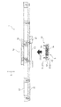
また、前記プローブカード11は、バネ性を有する複数本のプローブ3と、これら複数本のプローブ3を保持するプローブヘッド15と、を備えることによって構成されており、プローブ3は長尺な一例として円筒スリーブ状の筒体17(図2)と、該筒体17に挿入される長尺な一例として丸棒状のプランジャー(棒状体)19と、を備えることによって構成されている。
また、図示の実施形態では、前述したプローブヘッド15は、図3に表すようなカード構造12に対して直接、取り付けられるように構成されている。具体的には、クランプヘッド35とスティフナー37によって支持されたプリント基板39の一例として下面に固定リング41を使用して取り付けられたMLC(Multi Level Cell)43に、対して、下方から当該プローブヘッド15を挿し込んで固定ネジ45を締め付けることによってプローブヘッド15は取り付けられるように構成されている。
Further, the
Further, in the illustrated embodiment, the
そして、前記プリント基板39は、一例としてセラミックス基板と配線基板とが積層された多層構造の電子基板によって構成されており、前記プローブ3の基端部3aに入力端が接続されている前記MLC43の出力端に接続される。該配線路の他端は、前記プローブ3の先端部3bが前記被検査部7に接触し通電検査を行うことによって取得したデータに基づいて前述した各被検査部7の電気的特性の計測と被検査体5全体の動作試験を実行し、被検査体5の良否を判定する制御部23を備えるテスター25に接続されている。
As an example, the printed
(2)プローブカードの具体的構成(図2及び図4〜図6参照)
プローブカード11は、前述したようにバネ性を有するプローブ3と、該プローブ3を保持するプローブヘッド15と、を備えている。そして、プローブヘッド15には、プローブ3を押圧方向となる軸方向Zに移動可能に保持するガイド部27が設けられており、該ガイド部27には、通電により発生したプローブ3の熱を吸熱してプローブ3外に流す放熱構造29が備えられている。
(2) Specific configuration of probe card (see FIGS. 2 and 4 to 6)
As described above, the
(A)プローブの具体的構成(図5参照)
図2に表したように、プローブ3は、スリーブ状の案内筒部33の一部にバネ性を発現するバネ部31(31A、31B、31C、31D)を有する筒体17と、該筒体17に対して挿入され、前記案内筒部33の一部に接合されることによって該筒体17と一体になって軸方向Zに変位する導電性を有するプランジャー19と、を備えている。
また、本実施形態では、プローブ3のバネ性は、導電性を有する前記筒体17に設けられる螺旋状のスリット47によって形成されるバネ部31(31A、31B、31C、31D)によって付与されている。
(A) Specific configuration of probe (see FIG. 5)
As shown in FIG. 2, the
Further, in the present embodiment, the springiness of the
筒体17は、一例としてNiCo、NiPなどのニッケル合金製で外径が0.1mm以下で長さが6mm程度の極めて細い管材によって形成されており、軸方向Zの両端とその中間の4ヶ所に円筒スリーブ状の案内筒部33A、33B、33C、33Dが設けられている。また、これら4ヶ所の案内筒部33A、33B、33C、33Dの間の3ヶ所にプローブ3にバネ性を付与するバネ部31が設けられている。
尚、前記3ヶ所に設けられるバネ部31は一例として先端部3b寄りと基端部3a寄りに設けられている2本のバネ部31A、31Dが長く、その中央においてギャップGを隔てて設けられる2本のバネ部31B、31Cが短くなるように形成されている。また、前記ギャップGを境にして先端部3b側に配置されるバネ部31A、31Bと基端部3a側に配置されるバネ部31C、31Dの巻方向をそれぞれ逆にしており、これにより、プローブ3を押圧した時の筒体17の捩れを解消している。
As an example, the
As an example of the
更に、先端部3b寄りの案内筒部33Aと基端部3a寄りの案内筒部33Dには、軸方向Zに延びる所定長さの直線状の接合用スリット49A、49Bが対向する位置に1本ずつそれぞれ形成されている。因みに、この接合用スリット49A、49Bは、プランジャー19と筒体17とを抵抗溶接やカシメ等によって接合する際の筒体17の変形を防止して、一定の外径が保たれるようにする目的で形成されている。
また、前記バネ部31を設けるための螺旋状のスリット47の形成に当たっては、レーザー加工やエッチング処理等をそれぞれ単独で実施したり、両者を組み合わせて実施することが可能である。
Further, one of the
Further, in forming the spiral slit 47 for providing the
プランジャー19は、直径が0.05mm程度の丸棒状の部材で本実施形態では、先端部3b側に設けられる長さが4mm程度の第1プランジャー19Aと、基端部3a側に設けられる長さが2mm程度の第2プランジャー19Bと、の2本のプランジャーが使用されている。
このうち、第1プランジャー19Aは、一例としてAgPdCuなどのパラジウム合金製で、前記筒体17に組み付けた状態で該筒体17の先端部3b側の端面から1mm程度、先端が突出し、一方、第1プランジャー19Aの後端は、前記案内筒部33Cの内部に到達し得る長さに形成されている。
The
Of these, the
また、前記第1プランジャー19Aは、前述した案内筒部33Aに形成されている接合用スリット49Aの個所で筒体17に接合され、筒体17と一体になって軸方向Zに移動し得るように構成されている。
そして、前記第1プランジャー19Aの先端がプローブ3の先端部3bとなり、通電検査時において前述した被検査体5の被検査部7に接触するように構成されている。
Further, the
The tip of the
他方、第2プランジャー19Bは、一例としてタングステンやロジウム(Rh)或いはAgPdCuなどのパラジウム合金製で、前記筒体17に組み付けた状態で該筒体17の基端部3a側の端面から0.2mm程度、後端が突出し、一方、第2プランジャー19Bの先端は、前記案内筒部33Cの内部に到達し得る長さに形成されている。
また、前記第2プランジャー19Bは、前述した案内筒部33Dに形成されている接合用スリット49Bの個所で筒体17に接合され、筒体17と一体になって軸方向Zに移動し得るように構成されている。
On the other hand, the
Further, the
また、案内筒部33Cの内部に位置する第1プランジャー19Aの後端と第2プランジャー19Bの先端との間には、約0.4mmの間隙Sが形成されており、第1プランジャー19Aと第2プランジャー19Bを合わせて計0.4mmの移動ストロークが得られるように構成されている。
そして、前記第2プランジャー19Bの後端がプローブ3の基端部3aになり、前述したカード構造12のMLC43の入力側の接点に当接して、通電検査時において前述した各被検査部7の電気的特性等を出力できるように構成されている。
Further, a gap S of about 0.4 mm is formed between the rear end of the
Then, the rear end of the
(B)プローブヘッドの具体的構成(図2、図4及び図6参照)
プローブヘッド15は、本実施形態では、複数本のプローブ3と、プローブ3の基端部3a寄りの上部を保持する上部ガイド穴51aを有する上部ガイド部51と、プローブ3の先端部3b寄りの下部を保持する下部ガイド穴53aを有する下部ガイド部53と、前記上部ガイド部51と下部ガイド部53との中間に配置される中間スペーサー52と、前記上部ガイド部51と前記下部ガイド部53の間に位置し、上部ガイド部51、中間スペーサー52及び下部ガイド部53に形成された収容凹部55に収容される中間ガイド穴57aを有する中間ガイド部57と、を備えることによって構成されている。
(B) Specific configuration of probe head (see FIGS. 2, 4 and 6)
In the present embodiment, the
また、本実施形態では、前記中間ガイド部57がプローブ3の先端部3b側に位置する第1中間ガイド部57Aと、プローブ3の基端部3a側に位置する第3中間ガイド部57Cと、第1中間ガイド部57Aと第3中間ガイド部57Cの間に位置する第2中間ガイド部57Bの3つの中間ガイド部を備えることによって形成されている。
また、これら3つの中間ガイド部57A、57B、57Cの上面のプローブ3の設置範囲には所定深さの凹部57bがそれぞれ形成されており、前述した収容凹部55の底部に位置する下部ガイド部53にも収容凹部55の底面のプローブ3の設置範囲から所定深さの凹部53bが形成されている。
Further, in the present embodiment, the first
Further, a
そして、前述したプローブ3は、上部ガイド部51に形成されている上部ガイド穴51aに挿入された後、前記3つの中間ガイド部57A、57B、57Cにそれぞれ形成されている3つの凹部57bと複数の中間ガイド穴57aを通って、前記下部ガイド部53の凹部53bと下部ガイド穴53aに至り、プローブヘッド15の下面からプローブ3の先端部3bを所定長さ突出させた所定の位置で保持されるように構成されている。
Then, the
更に、本実施形態では、前述した3つの中間ガイド部57A、57B、57Cのすべてに放熱構造29を持たせており、該放熱構造29を持たせる手段として、前述した筒体17の4つのバネ部31A、31B、31C、31Dを囲うように対向して配置された3つの中間ガイド部57A、57B、57Cをプローブ3よりも熱伝導性の高い高熱伝導性材料で形成している。
そして、本実施形態では中間ガイド部57A、57B、57Cの材料としてセラミックスを採用している。また、セラミックスの中でも特に熱伝導率の高い窒化アルミニウム系のファインセラミックスが好適な材料として一例として使用できる。中間ガイド部57A、57B、57Cの材料として、ファインセラミック系、マシナブルセラミック系、樹脂系、ポリイミド系(フィルムのような薄いものではなく、厚さをもったもの)の材料等を使用することができる。これらの材料の一種類で又は複数種類を組み合わせた複合構造で用いてもよい。
尚、当該中間ガイド部57A、57B、57Cは、前記熱伝導性の他に、電気的絶縁性、放熱性、耐熱性が要求される仕様を満たす材料であり、また線膨張係数が低い材料であることが好ましい。
Further, in the present embodiment, all of the three
In this embodiment, ceramics are used as the material for the
The
また、放熱構造29としては、中間ガイド部57を高熱伝導性材料によって形成する他、プローブヘッド15内にエアレーション構造、水冷構造、ペルチェ構造等を設けることで構成してもよい。
Further, the
この他、本実施形態では、プローブ3の先端部3b寄りの部位を保持している下部ガイド部53と、プローブ3の基端部3a寄りの部位を保持している上部ガイド部51の材料としてもプローブ3よりも熱伝導性の高い高熱伝導性材料の一例としてセラミックスを使用しており、中間スペーサー52の材料として42アロイを一例として使用している。
In addition, in the present embodiment, the material of the
(3)プローブカードを使用して行う通電検査の内容(図7、図8参照)
次に、前記プローブカード11を備えた接触検査装置1を使用することによって実行される通電検査の内容をプローブ3の非通電時と通電時の動作を中心に説明する。
(A)非通電時(図7参照)
非通電時はプローブ3の先端部3bは、載置部9上に載置された被検査体5の被検査部7に対して離間した状態になっている。この状態では、バネ部31には負荷が掛かっていないため、第1プランジャー19Aの先端は筒体17の先端部3b側の端面から前述したように1mm程度突出した状態になっている。
(3) Contents of energization inspection performed using a probe card (see FIGS. 7 and 8)
Next, the contents of the energization inspection performed by using the contact inspection device 1 provided with the
(A) When not energized (see Fig. 7)
When the
(B)通電時(図8参照)
この状態から駆動部13を起動し、プローブ3の先端部3bを被検査部7に対して相対的に移動させて該被検査部7に接触させ、所定の押圧力で押し付ける。そして、プローブ3の先端部3bには被検査部7から基端部3a側に向けての反力が作用し、該反力の一部は第1プランジャー19Aと筒体17との接合点となる接合用スリット49Aが形成されている部位を介して案内筒部33Aを基端部3a側に押し上げるように作用する。
また、前記反力の一部か筒体17と第2プランジャー19Bとの接合点となる接合用スリット49Bが形成されている部位を介して案内筒部33Dを先端部3b側に押し下げるように作用する。そして、前記案内筒部33Aと案内筒部33Dの変位を4つのバネ部31A、31B、31C、31Dの圧縮変形によって吸収するように構成されている。
(B) When energized (see FIG. 8)
From this state, the
Further, the
また、プローブ3の先端部3bから第1プランジャー19Aを流れる電流は、案内筒部33A、バネ部31A、案内筒部33B、バネ部31B、ギャップG、バネ部31C、案内筒部33C、バネ部31D、案内筒部33D、第2プランジャー19Bの順で伝達されてプローブ3の基端部3aに至り、MLC43を介して、その電気信号が制御部23に送られる。
そして、この際、前記4つのバネ部31A、31B、31C、31Dがジュール熱により高温になるが、本実施形態ではこれらのバネ部31A、31B、31C、31Dと対向する位置の広い範囲に複数の中間ガイド部57A、57B、57Cが設けられているので、これらの中間ガイド部57A、57B、57Cが有する放熱作用が効果的に発揮されて該プローブ3の温度上昇が抑制される。即ち、前記バネ部31A、31B、31C、31Dは、それぞれ対向する位置に存する中間ガイド部57A、57B、57Cの中間ガイド穴57aの内周面によって前記ジュール熱を吸収されて放熱され、その温度上昇が抑制される。
Further, the current flowing from the
At this time, the four
そして、このようにして構成される本実施形態に係るプローブカード11及び接触検査装置1によれば、バネ性を有する導電性のプローブ3を使用して被検査体5の通電検査を行うに際して、高電流を印加して通電検査を行った場合でも、プローブ3の筒体17に設けられるバネ部31の温度上昇を抑制することができる。これにより、プローブ3のバネ性を低下させることなく通電検査を行うことができるから、通電検査の検査精度の低下を抑制することが可能になる。
Then, according to the
[他の実施形態]
本発明に係るプローブカード11及び接触検査装置1は、以上述べたような構成を有することを基本とするものであるが、本願発明の要旨を逸脱しない範囲内の部分的構成の変更や省略等を行うことも勿論可能である。
[Other embodiments]
The
例えば、放熱構造29は、プローブ3と対向する位置に存するすべてのガイド部27に設ける他、そのうち一部のガイド部27に対してだけ設けることも可能である。また、ガイド部27を構成している部材の全体に対して放熱構造29を適用する他、バネ部31と対向する位置に存するガイド部27の一部の範囲のみに放熱構造29を適用することも可能である。
また、前記実施形態では3つの中間ガイド部57A、57B、57Cを使用したが中間ガイド部57を4つ以上設けたり、中間ガイド部57を2つ以下に減らすことが可能である。
For example, the
Further, although three
1…接触検査装置、3…プローブ、3a…基端部、3b…先端部、5…被検査体、
7…被検査部、9…載置部、11…プローブカード、12…カード構造、
13…駆動部、15…プローブヘッド、17…筒体、19…プランジャー(棒状体)、
23…制御部、25…テスター、27…ガイド部、29…放熱構造、31…バネ部、
33…案内筒部、35…クランプヘッド、37…スティフナー、39…プリント基板、
41…固定リング、43…MLC、45…固定ネジ、47…スリット、
49A、49B…接合用スリット、51…上部ガイド部、51a…上部ガイド穴、
52…中間スペーサー、53…下部ガイド部、53a…下部ガイド穴、
53b…凹部、55…収容凹部、57…中間ガイド部、57a…中間ガイド穴、
57b…凹部、Z…軸方向、G…ギャップ、S…間隙
1 ... Contact inspection device, 3 ... Probe, 3a ... Base end, 3b ... Tip, 5 ... Inspected object,
7 ... Inspected part, 9 ... Placement part, 11 ... Probe card, 12 ... Card structure,
13 ... Drive unit, 15 ... Probe head, 17 ... Cylindrical body, 19 ... Plunger (rod-shaped body),
23 ... Control unit, 25 ... Tester, 27 ... Guide unit, 29 ... Heat dissipation structure, 31 ... Spring unit,
33 ... Guide tube, 35 ... Clamp head, 37 ... Stiffener, 39 ... Printed circuit board,
41 ... fixing ring, 43 ... MLC, 45 ... fixing screw, 47 ... slit,
49A, 49B ... Slit for joining, 51 ... Upper guide part, 51a ... Upper guide hole,
52 ... Intermediate spacer, 53 ... Lower guide part, 53a ... Lower guide hole,
53b ... recess, 55 ... storage recess, 57 ... intermediate guide, 57a ... intermediate guide hole,
57b ... concave, Z ... axial, G ... gap, S ... gap
Claims (6)
前記プローブを保持するプローブヘッドと、を備えるプローブカードであって、
前記プローブヘッドは、
前記プローブを軸方向にガイドしつつ移動可能に保持するガイド部を備え、
前記ガイド部は、通電により前記プローブで発生した熱を吸熱して該プローブ外に流す放熱構造を備え、更に、
前記プローブの上部を保持する上部ガイド穴を有する上部ガイド部と、
前記プローブの下部を軸方向にガイドしつつ移動可能に保持する下部ガイド穴を有する下部ガイド部と、
前記上部ガイド部と前記下部ガイド部の中間に位置し、前記プローブの中間部を軸方向にガイドしつつ移動可能に保持する中間ガイド穴を有する中間ガイド部と、を備え、
前記放熱構造を有するガイド部は、前記中間ガイド部であり、
前記放熱構造の吸熱部位の少なくとも一部は、前記プローブのバネ性を発現する部分と対向して位置する、
ことを特徴とするプローブカード。 With a probe with springiness,
A probe card including a probe head for holding the probe.
The probe head
A guide portion for holding the probe so as to be movable while guiding the probe in the axial direction is provided.
The guide portion has a heat radiating structure that absorbs heat generated by the probe by energization and flows it out of the probe.
An upper guide portion having an upper guide hole that holds the upper portion of said probe,
A lower guide portion having a lower guide hole that movably holds the lower portion of the probe while guiding it in the axial direction, and a lower guide portion.
It is provided with an intermediate guide portion located between the upper guide portion and the lower guide portion and having an intermediate guide hole for movably holding the intermediate portion of the probe while guiding it in the axial direction.
Guide unit having a heat dissipation structure, Ri the intermediate guide portion der,
At least a part of the endothermic portion of the heat dissipation structure is located so as to face the portion that exhibits the springiness of the probe.
A probe card characterized by that.
前記放熱構造は、前記ガイド部の前記プローブと対向する部分の少なくとも一部が、前記プローブで発生した熱を該プローブから遠ざかる方向に放熱、拡散させる高熱伝導性材料で形成された構成である、ことを特徴とするプローブカード。 In the probe card according to claim 1,
The heat dissipation structure has a structure in which at least a part of the guide portion facing the probe is made of a highly thermally conductive material that dissipates and diffuses heat generated by the probe in a direction away from the probe. A probe card characterized by that.
前記放熱構造を有するガイド部は、上下方向に複数に分割されている、ことを特徴とするプローブカード。 In the probe card according to claim 1 or 2.
A probe card characterized in that the guide portion having the heat dissipation structure is divided into a plurality of parts in the vertical direction.
前記プローブのバネ性は、該プローブを構成する導電性の筒体に設けられたスリットによって付与されている、ことを特徴とするプローブカード。 In the probe card according to any one of claims 1 to 3.
A probe card characterized in that the springiness of the probe is imparted by a slit provided in a conductive cylinder constituting the probe.
前記プローブは、スリーブ状の案内筒部の一部にバネ性を発現するバネ部を有する筒体と、
前記筒体に対して挿入され、前記案内筒部の一部に接合されることによって筒体と一体になって軸方向に変位する導電性を有する棒状体と、を備えている、ことを特徴とするプローブカード。 In the probe card according to claim 4,
The probe includes a tubular body having a spring portion that exhibits springiness in a part of a sleeve-shaped guide tubular portion, and a tubular body.
It is characterized by having a rod-shaped body having conductivity which is inserted into the tubular body and joined to a part of the guide tubular portion to be integrated with the tubular body and displaced in the axial direction. Probe card.
バネ性を有するプローブを備えるプローブカードと、
前記載置部上の被検査体の被検査部と前記プローブカードとの相対位置を接離可能に変化させる駆動部と、を備え、
前記載置部上に載置された被検査体の被検査部に対して、前記プローブが接触することによって通電検査を行う接触検査装置であって、
前記プローブカードは、請求項1から5のいずれか一項に記載されたプローブカードである、ことを特徴とする接触検査装置。
The mounting part on which the object to be inspected is placed and
A probe card with a springy probe and
It is provided with a drive unit that changes the relative position of the probe card to be inspected and the probe card to be inspected on the above-mentioned place.
A contact inspection device that performs an energization inspection by contacting the probe with the inspected portion of the inspected body placed on the above-mentioned placement portion.
The contact inspection device, wherein the probe card is the probe card according to any one of claims 1 to 5.
Priority Applications (7)
| Application Number | Priority Date | Filing Date | Title |
|---|---|---|---|
| JP2015207263A JP6890921B2 (en) | 2015-10-21 | 2015-10-21 | Probe card and contact inspection device |
| CN201680061723.XA CN108351371B (en) | 2015-10-21 | 2016-10-13 | Probe card and contact inspection apparatus |
| US15/770,062 US10775411B2 (en) | 2015-10-21 | 2016-10-13 | Probe card and contact inspection device |
| EP16857343.4A EP3367108A4 (en) | 2015-10-21 | 2016-10-13 | Probe card and contact inspection device |
| PCT/JP2016/080301 WO2017069028A1 (en) | 2015-10-21 | 2016-10-13 | Probe card and contact inspection device |
| KR1020187011736A KR102015741B1 (en) | 2015-10-21 | 2016-10-13 | Probe card and contact inspection device |
| TW105133572A TWI627413B (en) | 2015-10-21 | 2016-10-18 | Probe card and contact inspection device |
Applications Claiming Priority (1)
| Application Number | Priority Date | Filing Date | Title |
|---|---|---|---|
| JP2015207263A JP6890921B2 (en) | 2015-10-21 | 2015-10-21 | Probe card and contact inspection device |
Publications (3)
| Publication Number | Publication Date |
|---|---|
| JP2017078660A JP2017078660A (en) | 2017-04-27 |
| JP2017078660A5 JP2017078660A5 (en) | 2018-10-11 |
| JP6890921B2 true JP6890921B2 (en) | 2021-06-18 |
Family
ID=58557432
Family Applications (1)
| Application Number | Title | Priority Date | Filing Date |
|---|---|---|---|
| JP2015207263A Active JP6890921B2 (en) | 2015-10-21 | 2015-10-21 | Probe card and contact inspection device |
Country Status (7)
| Country | Link |
|---|---|
| US (1) | US10775411B2 (en) |
| EP (1) | EP3367108A4 (en) |
| JP (1) | JP6890921B2 (en) |
| KR (1) | KR102015741B1 (en) |
| CN (1) | CN108351371B (en) |
| TW (1) | TWI627413B (en) |
| WO (1) | WO2017069028A1 (en) |
Families Citing this family (14)
| Publication number | Priority date | Publication date | Assignee | Title |
|---|---|---|---|---|
| JP6892277B2 (en) * | 2017-02-10 | 2021-06-23 | 株式会社日本マイクロニクス | Probes and electrical connections |
| JP6980410B2 (en) * | 2017-05-23 | 2021-12-15 | 株式会社日本マイクロニクス | probe |
| JP7075725B2 (en) | 2017-05-30 | 2022-05-26 | 株式会社日本マイクロニクス | Electrical connection device |
| US10566256B2 (en) * | 2018-01-04 | 2020-02-18 | Winway Technology Co., Ltd. | Testing method for testing wafer level chip scale packages |
| US11467186B2 (en) * | 2018-08-23 | 2022-10-11 | Nidec-Read Corporation | Inspection jig, inspection device, and contact terminal |
| KR102037657B1 (en) | 2018-09-05 | 2019-10-29 | 주식회사 아이에스시 | Probe card for electrical test and probe head for probe card |
| TW202032137A (en) * | 2019-02-22 | 2020-09-01 | 日商日本電產理德股份有限公司 | Test jig |
| KR102037198B1 (en) | 2019-06-16 | 2019-10-28 | 심민섭 | Probe card inspection device |
| CN112240945A (en) * | 2019-07-17 | 2021-01-19 | 中华精测科技股份有限公司 | Improved structure of wafer probe card |
| JP7148472B2 (en) * | 2019-09-27 | 2022-10-05 | 株式会社フェローテックマテリアルテクノロジーズ | Ceramic part and method for manufacturing ceramic part |
| KR20210098090A (en) * | 2020-01-31 | 2021-08-10 | (주)포인트엔지니어링 | Probe head and probe card having the same |
| JP7175518B2 (en) * | 2020-06-02 | 2022-11-21 | 東理システム株式会社 | Electrical characteristic inspection unit device for power conversion circuit devices |
| JP2022116470A (en) * | 2021-01-29 | 2022-08-10 | 株式会社村田製作所 | Probe device |
| KR20230127485A (en) * | 2022-02-25 | 2023-09-01 | (주)티에스이 | Lower Friction Probe Head |
Family Cites Families (27)
| Publication number | Priority date | Publication date | Assignee | Title |
|---|---|---|---|---|
| JP2556245B2 (en) * | 1992-11-27 | 1996-11-20 | 日本電気株式会社 | Probe card |
| JP3530518B2 (en) * | 2002-01-24 | 2004-05-24 | 日本電子材料株式会社 | Probe card |
| JP4455940B2 (en) | 2004-06-17 | 2010-04-21 | 株式会社日本マイクロニクス | Electrical connection device |
| JP4598614B2 (en) * | 2005-06-30 | 2010-12-15 | 富士通株式会社 | Socket and electronic equipment |
| JP2007057444A (en) * | 2005-08-25 | 2007-03-08 | Nidec-Read Corp | Board inspection device and temperature maintenance mechanism for same |
| US7601009B2 (en) * | 2006-05-18 | 2009-10-13 | Centipede Systems, Inc. | Socket for an electronic device |
| JP2008243861A (en) * | 2007-03-23 | 2008-10-09 | Tokyo Electron Ltd | Inspection apparatus and method |
| JP2009162483A (en) | 2007-12-28 | 2009-07-23 | Micronics Japan Co Ltd | Electrical connection device |
| JP5056518B2 (en) * | 2008-03-19 | 2012-10-24 | 富士通株式会社 | Electronic unit |
| JP2009276215A (en) * | 2008-05-15 | 2009-11-26 | Tokyo Electron Ltd | Probe apparatus and method for correcting contact position |
| JP5222038B2 (en) * | 2008-06-20 | 2013-06-26 | 東京エレクトロン株式会社 | Probe device |
| CN201293798Y (en) * | 2008-10-31 | 2009-08-19 | 中茂电子(深圳)有限公司 | Probe card for solar battery detection bench |
| JP5903888B2 (en) | 2010-03-15 | 2016-04-13 | 日本電産リード株式会社 | Connection terminal and inspection jig |
| JP5826466B2 (en) * | 2010-06-25 | 2015-12-02 | 東京エレクトロン株式会社 | Probe card parallel adjustment mechanism and inspection device |
| US9000792B2 (en) * | 2010-09-21 | 2015-04-07 | Hideo Nishikawa | Inspection jig and contact |
| WO2013051099A1 (en) * | 2011-10-04 | 2013-04-11 | 富士通株式会社 | Testing jig and semiconductor device test method |
| SG11201401212TA (en) * | 2011-10-07 | 2014-09-26 | Nhk Spring Co Ltd | Probe unit |
| JP6092509B2 (en) * | 2011-10-17 | 2017-03-08 | 東京エレクトロン株式会社 | Contact terminal support and probe card |
| JP2014025737A (en) * | 2012-07-25 | 2014-02-06 | Nidec-Read Corp | Inspecting tool and contact |
| JP5847663B2 (en) | 2012-08-01 | 2016-01-27 | 日本電子材料株式会社 | Manufacturing method of probe card guide plate |
| JP6017228B2 (en) | 2012-08-27 | 2016-10-26 | 株式会社日本マイクロニクス | Electrical connection device |
| JP2014048266A (en) * | 2012-09-04 | 2014-03-17 | Toshiba Corp | Probe card, and test method and test device of imaging device using the same |
| JP6235785B2 (en) * | 2013-03-18 | 2017-11-22 | 日本電子材料株式会社 | Probe card guide plate and probe card guide plate manufacturing method |
| TWI548879B (en) * | 2014-01-28 | 2016-09-11 | Spring sleeve probe | |
| JP6546719B2 (en) | 2014-02-07 | 2019-07-17 | 株式会社日本マイクロニクス | Contact inspection device |
| TW201533449A (en) * | 2014-02-24 | 2015-09-01 | Mpi Corp | Probing device with spring-barrel probe |
| TWI570415B (en) * | 2015-10-02 | 2017-02-11 | A spring probe having an outer sleeve and a probe device having the spring probe |
-
2015
- 2015-10-21 JP JP2015207263A patent/JP6890921B2/en active Active
-
2016
- 2016-10-13 CN CN201680061723.XA patent/CN108351371B/en active Active
- 2016-10-13 WO PCT/JP2016/080301 patent/WO2017069028A1/en active Application Filing
- 2016-10-13 US US15/770,062 patent/US10775411B2/en active Active
- 2016-10-13 EP EP16857343.4A patent/EP3367108A4/en active Pending
- 2016-10-13 KR KR1020187011736A patent/KR102015741B1/en active IP Right Grant
- 2016-10-18 TW TW105133572A patent/TWI627413B/en active
Also Published As
| Publication number | Publication date |
|---|---|
| US10775411B2 (en) | 2020-09-15 |
| TWI627413B (en) | 2018-06-21 |
| EP3367108A4 (en) | 2019-06-19 |
| KR102015741B1 (en) | 2019-08-28 |
| TW201728908A (en) | 2017-08-16 |
| US20180299489A1 (en) | 2018-10-18 |
| WO2017069028A1 (en) | 2017-04-27 |
| CN108351371B (en) | 2021-04-27 |
| KR20180059867A (en) | 2018-06-05 |
| EP3367108A1 (en) | 2018-08-29 |
| JP2017078660A (en) | 2017-04-27 |
| CN108351371A (en) | 2018-07-31 |
Similar Documents
| Publication | Publication Date | Title |
|---|---|---|
| JP6890921B2 (en) | Probe card and contact inspection device | |
| KR101381564B1 (en) | Inspection apparatus for semiconductor devices and chunk stage used for the inspection apparatus | |
| US6967492B2 (en) | Spring contact probe device for electrical testing | |
| TWI502204B (en) | Electric connecting apparatus | |
| JP2017078660A5 (en) | ||
| CN107037346B (en) | Evaluation device and evaluation method for semiconductor device | |
| JP6209375B2 (en) | Electrical connection device | |
| JPS63179266A (en) | Method and device for measuring thermal resistance of element such as part with high-density integrated circuit | |
| US10495668B2 (en) | Evaluation apparatus for semiconductor device and evaluation method for semiconductor device | |
| JP2020517914A (en) | Probe card for electronic device test equipment | |
| US11454601B2 (en) | Substrate evaluation chip and substrate evaluation device | |
| JP2017009449A (en) | Contact probe type temperature detector, evaluation device of semiconductor device and evaluation method of semiconductor device | |
| JP2007234950A (en) | Heat sink with temperature sensor | |
| JP6365953B1 (en) | Prober | |
| JP4679059B2 (en) | Power semiconductor device test apparatus and test method using the same | |
| JP6313131B2 (en) | Humidity sensor inspection device | |
| TWI646333B (en) | Probe and electrical connection device | |
| JP5748709B2 (en) | Probe card | |
| JP5290820B2 (en) | Electronic component measuring apparatus and measuring method | |
| JP2008010633A (en) | Prober | |
| KR20140105897A (en) | Probe card and apparatus for testing an object including the same | |
| JP2022080072A (en) | Wafer chuck and prober device | |
| JP2008232958A (en) | Inspection tool and semiconductor device inspection method |
Legal Events
| Date | Code | Title | Description |
|---|---|---|---|
| A521 | Written amendment |
Free format text: JAPANESE INTERMEDIATE CODE: A523 Effective date: 20180823 |
|
| A621 | Written request for application examination |
Free format text: JAPANESE INTERMEDIATE CODE: A621 Effective date: 20180823 |
|
| A131 | Notification of reasons for refusal |
Free format text: JAPANESE INTERMEDIATE CODE: A131 Effective date: 20190829 |
|
| A521 | Written amendment |
Free format text: JAPANESE INTERMEDIATE CODE: A523 Effective date: 20191023 |
|
| A02 | Decision of refusal |
Free format text: JAPANESE INTERMEDIATE CODE: A02 Effective date: 20200402 |
|
| A521 | Written amendment |
Free format text: JAPANESE INTERMEDIATE CODE: A523 Effective date: 20200529 |
|
| C60 | Trial request (containing other claim documents, opposition documents) |
Free format text: JAPANESE INTERMEDIATE CODE: C60 Effective date: 20200529 |
|
| A911 | Transfer to examiner for re-examination before appeal (zenchi) |
Free format text: JAPANESE INTERMEDIATE CODE: A911 Effective date: 20200608 |
|
| C21 | Notice of transfer of a case for reconsideration by examiners before appeal proceedings |
Free format text: JAPANESE INTERMEDIATE CODE: C21 Effective date: 20200610 |
|
| A912 | Re-examination (zenchi) completed and case transferred to appeal board |
Free format text: JAPANESE INTERMEDIATE CODE: A912 Effective date: 20200828 |
|
| C211 | Notice of termination of reconsideration by examiners before appeal proceedings |
Free format text: JAPANESE INTERMEDIATE CODE: C211 Effective date: 20200902 |
|
| C22 | Notice of designation (change) of administrative judge |
Free format text: JAPANESE INTERMEDIATE CODE: C22 Effective date: 20201118 |
|
| C13 | Notice of reasons for refusal |
Free format text: JAPANESE INTERMEDIATE CODE: C13 Effective date: 20210203 |
|
| A521 | Written amendment |
Free format text: JAPANESE INTERMEDIATE CODE: A523 Effective date: 20210222 |
|
| C23 | Notice of termination of proceedings |
Free format text: JAPANESE INTERMEDIATE CODE: C23 Effective date: 20210407 |
|
| C03 | Trial/appeal decision taken |
Free format text: JAPANESE INTERMEDIATE CODE: C03 Effective date: 20210511 |
|
| C30A | Notification sent |
Free format text: JAPANESE INTERMEDIATE CODE: C3012 Effective date: 20210511 |
|
| A61 | First payment of annual fees (during grant procedure) |
Free format text: JAPANESE INTERMEDIATE CODE: A61 Effective date: 20210526 |
|
| R150 | Certificate of patent or registration of utility model |
Ref document number: 6890921 Country of ref document: JP Free format text: JAPANESE INTERMEDIATE CODE: R150 |