WO2017069028A1 - Probe card and contact inspection device - Google Patents
Probe card and contact inspection device Download PDFInfo
- Publication number
- WO2017069028A1 WO2017069028A1 PCT/JP2016/080301 JP2016080301W WO2017069028A1 WO 2017069028 A1 WO2017069028 A1 WO 2017069028A1 JP 2016080301 W JP2016080301 W JP 2016080301W WO 2017069028 A1 WO2017069028 A1 WO 2017069028A1
- Authority
- WO
- WIPO (PCT)
- Prior art keywords
- probe
- probe card
- guide
- card according
- spring
- Prior art date
Links
Images


Classifications
-
- G—PHYSICS
- G01—MEASURING; TESTING
- G01R—MEASURING ELECTRIC VARIABLES; MEASURING MAGNETIC VARIABLES
- G01R1/00—Details of instruments or arrangements of the types included in groups G01R5/00 - G01R13/00 and G01R31/00
- G01R1/02—General constructional details
- G01R1/06—Measuring leads; Measuring probes
- G01R1/067—Measuring probes
- G01R1/073—Multiple probes
- G01R1/07307—Multiple probes with individual probe elements, e.g. needles, cantilever beams or bump contacts, fixed in relation to each other, e.g. bed of nails fixture or probe card
- G01R1/07314—Multiple probes with individual probe elements, e.g. needles, cantilever beams or bump contacts, fixed in relation to each other, e.g. bed of nails fixture or probe card the body of the probe being perpendicular to test object, e.g. bed of nails or probe with bump contacts on a rigid support
-
- G—PHYSICS
- G01—MEASURING; TESTING
- G01R—MEASURING ELECTRIC VARIABLES; MEASURING MAGNETIC VARIABLES
- G01R1/00—Details of instruments or arrangements of the types included in groups G01R5/00 - G01R13/00 and G01R31/00
- G01R1/02—General constructional details
- G01R1/06—Measuring leads; Measuring probes
- G01R1/067—Measuring probes
- G01R1/06705—Apparatus for holding or moving single probes
-
- G—PHYSICS
- G01—MEASURING; TESTING
- G01R—MEASURING ELECTRIC VARIABLES; MEASURING MAGNETIC VARIABLES
- G01R1/00—Details of instruments or arrangements of the types included in groups G01R5/00 - G01R13/00 and G01R31/00
- G01R1/02—General constructional details
- G01R1/06—Measuring leads; Measuring probes
- G01R1/067—Measuring probes
- G01R1/06711—Probe needles; Cantilever beams; "Bump" contacts; Replaceable probe pins
- G01R1/06716—Elastic
-
- G—PHYSICS
- G01—MEASURING; TESTING
- G01R—MEASURING ELECTRIC VARIABLES; MEASURING MAGNETIC VARIABLES
- G01R1/00—Details of instruments or arrangements of the types included in groups G01R5/00 - G01R13/00 and G01R31/00
- G01R1/02—General constructional details
- G01R1/06—Measuring leads; Measuring probes
- G01R1/067—Measuring probes
- G01R1/06711—Probe needles; Cantilever beams; "Bump" contacts; Replaceable probe pins
- G01R1/06733—Geometry aspects
-
- G—PHYSICS
- G01—MEASURING; TESTING
- G01R—MEASURING ELECTRIC VARIABLES; MEASURING MAGNETIC VARIABLES
- G01R1/00—Details of instruments or arrangements of the types included in groups G01R5/00 - G01R13/00 and G01R31/00
- G01R1/02—General constructional details
- G01R1/06—Measuring leads; Measuring probes
- G01R1/067—Measuring probes
- G01R1/073—Multiple probes
- G01R1/07307—Multiple probes with individual probe elements, e.g. needles, cantilever beams or bump contacts, fixed in relation to each other, e.g. bed of nails fixture or probe card
- G01R1/07314—Multiple probes with individual probe elements, e.g. needles, cantilever beams or bump contacts, fixed in relation to each other, e.g. bed of nails fixture or probe card the body of the probe being perpendicular to test object, e.g. bed of nails or probe with bump contacts on a rigid support
- G01R1/07328—Multiple probes with individual probe elements, e.g. needles, cantilever beams or bump contacts, fixed in relation to each other, e.g. bed of nails fixture or probe card the body of the probe being perpendicular to test object, e.g. bed of nails or probe with bump contacts on a rigid support for testing printed circuit boards
-
- G—PHYSICS
- G01—MEASURING; TESTING
- G01R—MEASURING ELECTRIC VARIABLES; MEASURING MAGNETIC VARIABLES
- G01R1/00—Details of instruments or arrangements of the types included in groups G01R5/00 - G01R13/00 and G01R31/00
- G01R1/02—General constructional details
- G01R1/06—Measuring leads; Measuring probes
- G01R1/067—Measuring probes
- G01R1/073—Multiple probes
- G01R1/07307—Multiple probes with individual probe elements, e.g. needles, cantilever beams or bump contacts, fixed in relation to each other, e.g. bed of nails fixture or probe card
- G01R1/07364—Multiple probes with individual probe elements, e.g. needles, cantilever beams or bump contacts, fixed in relation to each other, e.g. bed of nails fixture or probe card with provisions for altering position, number or connection of probe tips; Adapting to differences in pitch
- G01R1/07371—Multiple probes with individual probe elements, e.g. needles, cantilever beams or bump contacts, fixed in relation to each other, e.g. bed of nails fixture or probe card with provisions for altering position, number or connection of probe tips; Adapting to differences in pitch using an intermediate card or back card with apertures through which the probes pass
-
- G—PHYSICS
- G01—MEASURING; TESTING
- G01R—MEASURING ELECTRIC VARIABLES; MEASURING MAGNETIC VARIABLES
- G01R31/00—Arrangements for testing electric properties; Arrangements for locating electric faults; Arrangements for electrical testing characterised by what is being tested not provided for elsewhere
- G01R31/28—Testing of electronic circuits, e.g. by signal tracer
- G01R31/2851—Testing of integrated circuits [IC]
- G01R31/2886—Features relating to contacting the IC under test, e.g. probe heads; chucks
-
- G—PHYSICS
- G01—MEASURING; TESTING
- G01R—MEASURING ELECTRIC VARIABLES; MEASURING MAGNETIC VARIABLES
- G01R1/00—Details of instruments or arrangements of the types included in groups G01R5/00 - G01R13/00 and G01R31/00
- G01R1/02—General constructional details
- G01R1/06—Measuring leads; Measuring probes
- G01R1/067—Measuring probes
- G01R1/06711—Probe needles; Cantilever beams; "Bump" contacts; Replaceable probe pins
- G01R1/06716—Elastic
- G01R1/06722—Spring-loaded
-
- G—PHYSICS
- G01—MEASURING; TESTING
- G01R—MEASURING ELECTRIC VARIABLES; MEASURING MAGNETIC VARIABLES
- G01R1/00—Details of instruments or arrangements of the types included in groups G01R5/00 - G01R13/00 and G01R31/00
- G01R1/02—General constructional details
- G01R1/06—Measuring leads; Measuring probes
- G01R1/067—Measuring probes
- G01R1/06777—High voltage probes
-
- G—PHYSICS
- G01—MEASURING; TESTING
- G01R—MEASURING ELECTRIC VARIABLES; MEASURING MAGNETIC VARIABLES
- G01R31/00—Arrangements for testing electric properties; Arrangements for locating electric faults; Arrangements for electrical testing characterised by what is being tested not provided for elsewhere
- G01R31/28—Testing of electronic circuits, e.g. by signal tracer
- G01R31/2851—Testing of integrated circuits [IC]
- G01R31/2886—Features relating to contacting the IC under test, e.g. probe heads; chucks
- G01R31/2887—Features relating to contacting the IC under test, e.g. probe heads; chucks involving moving the probe head or the IC under test; docking stations
Definitions
- the present invention relates to a probe card used for an energization test of a semiconductor integrated circuit and a contact inspection apparatus including the probe card.
- the contact inspection device is in an electrically connected state by pressing with a suitable pressing force using the spring property in a state in which a conductive probe having spring property is brought into contact with a portion to be inspected.
- Establish. A device that conducts and inspects in this state is a contact inspection device.
- apparatuses described in Patent Documents 1 to 4 can be cited.
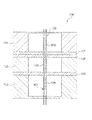
- FIG. 9 shows the structure of a conventional probe head 100.
- the probe head 100 is basically composed of seven parts including a probe 101, a lower plate 102, an intermediate spacer 103, an upper plate 104, a first intermediate guide film 105, a second intermediate guide film 106, and a third intermediate guide film 107. It is configured.
- the straightness of the probe 101 is maintained by being held by five members of the lower plate 102, the upper plate 104, the first intermediate guide film 105, the second intermediate guide film 106, and the third intermediate guide film 107.
- the range held by the first intermediate guide film 105, the second intermediate guide film 106, and the third intermediate guide film 107 was set to a narrow range excluding the portion 108 that exhibits the spring action of the probe 101. .
- JP 2009-162483 A JP 2006-3191 A JP 2014-44099 A JP2015-148561A
- An object of the present invention is to provide a probe card that conducts an energization inspection of an object to be inspected using a conductive probe having a spring property, and a contact inspection apparatus including the probe card, when a high current is applied during the energization inspection. However, this is to reduce the possibility that the spring property of the probe will be lowered.
- a probe card is a probe card including a probe having a spring property and a probe head that holds the probe, and the probe head includes the probe
- the guide portion is provided with a heat radiating structure that absorbs the probe heat generated by energization and flows the probe heat out of the probe.
- the guide portion has a heat dissipation structure that absorbs the heat of the probe and flows it out of the probe.
- a heat dissipation structure that absorbs the heat of the probe and flows it out of the probe.
- the probe card according to a second aspect of the present invention is the probe card according to the first aspect, wherein at least a part of a portion of the guide portion facing the probe keeps the heat generated by the probe away from the probe. It is characterized by having a structure formed of a high thermal conductivity material that dissipates and diffuses in the direction.
- specific examples of the high thermal conductivity material include fine ceramic materials, machinable ceramic materials, resin materials, and polyimide materials (thickness, not as thin as a film). It is done. These materials may be used alone or in a composite structure combining a plurality of types.
- the guide portion preferably satisfies the required specifications for electrical insulation, heat dissipation, and heat resistance, and is preferably a material having a low coefficient of linear expansion.
- the heat dissipation structure is formed of a high thermal conductivity material that at least part of the portion of the guide portion facing the probe dissipates and diffuses the heat generated by the probe in a direction away from the probe.
- This is the configuration.
- the Joule heat can be easily absorbed and dissipated by the guide portion formed of the high thermal conductivity material while the guide portion guides the movement of the probe during the energization inspection. Thereby, the high temperature of the probe is suppressed, and the possibility that the spring property of the probe is lowered can be reduced.
- the heat dissipation structure can be constructed with a simple structure.
- the heat dissipation structure is not limited to a structure using the high thermal conductivity material.
- the probe card according to a third aspect of the present invention is the probe card according to the first aspect or the second aspect, wherein at least a part of the heat absorbing portion of the heat dissipation structure is positioned to face a portion that expresses the spring property of the probe. It is characterized by that.
- the heat absorbing portion of the heat dissipation structure since at least a part of the heat absorbing portion of the heat dissipation structure is located opposite to the portion that exhibits the spring property of the probe, Joule heat that is generated directly from the portion that exhibits the spring property of the probe. Therefore, it is possible to effectively suppress a decrease in the spring property of the probe. In addition, since Joule heat can be effectively absorbed, the temperature rise of the probe can be suppressed, and the possibility that the spring property of the probe is lowered can be reduced.
- the probe card according to a fourth aspect of the present invention is the probe card according to any one of the first to third aspects, wherein the probe head includes an upper guide portion having an upper guide hole for holding an upper portion of the probe; A lower guide portion having a lower guide hole for holding the lower portion of the probe, and an intermediate guide portion having an intermediate guide hole that is located between the upper guide portion and the lower guide portion and holds the intermediate portion of the probe.
- the guide part having the heat dissipation structure is the intermediate guide part.
- the probe is guided by the plurality of guide parts constituted by the upper guide part, the lower guide part, and the intermediate guide part located in the middle, the movement of the probe during the energization inspection is enhanced. While guiding with accuracy, the temperature of the probe is prevented from being increased, and the possibility that the spring property of the probe is lowered can be reduced.
- the probe card according to a fifth aspect of the present invention is characterized in that, in the fourth aspect, the guide portion having the heat dissipation structure is divided into a plurality of parts in the vertical direction.
- the intermediate guide portion (the portion having the intermediate guide hole) having the heat dissipation structure is divided into a plurality of parts in the vertical direction, so that the probe can be easily assembled and the productivity of the probe card is improved. To do.
- the probe card according to a sixth aspect of the present invention is the probe card according to any one of the first to fifth aspects, wherein the spring property of the probe is provided in a conductive cylinder constituting the probe. It is provided by the slit.
- a probe card according to a seventh aspect of the present invention is the probe card according to the sixth aspect, wherein the probe is a cylinder having a spring portion that expresses a spring property in a part of a sleeve-shaped guide cylinder, and the cylinder And a conductive rod-like body that is integrated with the cylinder body and is displaced in the axial direction by being joined to a part of the guide cylinder portion.
- the same action as the eighth aspect It is possible to effectively suppress the effect, that is, the decrease in springiness due to the high temperature of the probe.
- a contact inspection apparatus includes a placement portion on which an object to be inspected is placed, a probe card including a probe having a spring property, and a portion to be inspected on the placement portion. And a drive unit that changes the relative position between the probe card and the probe card so that the probe card comes into contact with the probe card.
- the action and effect of any one of the first to seventh aspects of the probe card are applied to the contact inspection device, and the spring property is lowered due to the high temperature of the probe. Can be effectively suppressed and the inspection accuracy of the contact inspection apparatus can be improved.
- FIGS. 1 and 3 an outline of the contact inspection apparatus according to the embodiment of the present invention will be described based on FIGS. 1 and 3.
- FIGS. 7A and 7B the contents of the energization inspection performed using the probe card will be described with reference to FIGS. 7A and 7B, focusing on the operation when the probe is not energized and when the probe is energized.
- the contact inspection apparatus 1 is electrically operated by pressing the conductive probe 3 having a spring property with an appropriate pressing force using the spring property in a state where the probe 3 is in contact with the inspected portion 7 of the inspection object 5.
- a general connection state In this state, the probe 3 is turned on to measure the electrical characteristics such as the current value and the voltage difference of each part 7 to be inspected, or an operation test of the whole body 5 to be inspected is performed.
- the contact inspection apparatus 1 is used for the purpose of determining the above.
- the inspected object 5 to be inspected by the contact inspection apparatus 1 examples include an electronic substrate such as a printed wiring board, a semiconductor wafer, or a semiconductor chip such as a packaged IC or LSI.
- the inspected portion 7 with which the probe 3 directly contacts is an inspection pattern or electrode on an electronic circuit mounted on an electronic substrate or the like.
- the surface of the portion to be inspected 7 such as the electrode is usually covered with an oxide film during inspection.
- the contact inspection apparatus 1 includes a placement unit 9 on which the above-described inspected object 5 is placed, a probe card 11 of the present invention including a probe 3 having a spring property, and the placement unit 9 described above. This is basically configured by including a drive unit 13 that changes the relative position between the inspected part 7 of the inspected object 5 and the probe card 11 so as to be able to contact and separate.
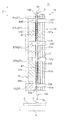
- the probe card 11 includes a plurality of probes 3 having spring properties and a probe head 15 that holds the plurality of probes 3.
- the probe 3 is a long example.
- a cylindrical sleeve-like cylindrical body 17 (FIG. 2) and a round bar-like plunger (bar-shaped body) 19 as a long example inserted into the cylindrical body 17 are provided.
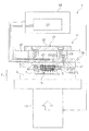
- the probe head 15 described above is configured to be directly attached to the card structure 12 as shown in FIG.
- an MLC (Multi Level Cell) 43 attached to the lower surface using a fixing ring 41 is used from the lower side to the probe head.
- the probe head 15 is configured to be attached by inserting 15 and tightening the fixing screw 45.
- the printed circuit board 39 is configured by an electronic substrate having a multilayer structure in which a ceramic substrate and a wiring substrate are laminated, and the input end of the MLC 43 is connected to the base end portion 3a of the probe 3. Connected to the output terminal.
- the other end of the wiring path is the measurement of the electrical characteristics of each of the inspected portions 7 described above based on the data acquired by the tip portion 3b of the probe 3 coming into contact with the inspected portion 7 and conducting an electric current inspection. It is connected to a tester 25 including a control unit 23 that performs an operation test of the entire inspection object 5 and determines whether the inspection object 5 is good or bad.
- the probe card 11 includes the probe 3 having spring properties and the probe head 15 that holds the probe 3.
- the probe head 15 is provided with a guide portion 27 that holds the probe 3 so as to be movable in the axial direction Z as a pressing direction.
- the guide portion 27 absorbs heat of the probe 3 generated by energization.
- a heat dissipation structure 29 that flows outside the probe 3 is provided.
- the probe 3 includes a cylindrical body 17 having a spring portion 31 (31 ⁇ / b> A, 31 ⁇ / b> B, 31 ⁇ / b> C, 31 ⁇ / b> D) that expresses a spring property in a part of a sleeve-shaped guide cylindrical portion 33, and the cylindrical body.
- a plunger (rod-like body) 19 having conductivity which is inserted into the guide cylinder portion 17 and joined to a part of the guide cylinder portion 33 so as to be integrated with the cylinder body 17 and displaced in the axial direction Z.
- the spring property of the probe 3 is provided by the spring portion 31 (31A, 31B, 31C, 31D) formed by the spiral slit 47 provided in the cylindrical body 17 having conductivity. Yes.
- the cylindrical body 17 is made of, for example, a nickel alloy such as NiCo, NiP, etc., and is formed of an extremely thin tube material having an outer diameter of 0.1 mm or less and a length of about 6 mm.
- spring portions 31 for imparting spring properties to the probe 3 are provided at three locations between the four guide tube portions 33A, 33B, 33C, and 33D.
- the spring portions 31 provided at the three locations are, for example, two spring portions 31A and 31D provided near the distal end portion 3b and the proximal end portion 3a, and are provided with a gap G at the center.
- the two spring portions 31B and 31C are formed to be short.
- the guide tube portion 33A near the distal end portion 3b and the guide tube portion 33D near the base end portion 3a are each provided with a linear joining slit 49A, 49B having a predetermined length extending in the axial direction Z. Each one is formed.
- the joining slits 49A and 49B prevent deformation of the cylindrical body 17 when the plunger 19 and the cylindrical body 17 are joined by resistance welding, caulking or the like so that a constant outer diameter is maintained. It is formed for the purpose of.
- the spiral slit 47 for providing the spring portion 31 it is possible to carry out laser processing, etching processing or the like alone or in combination.
- the plunger 19 is a round bar-like member having a diameter of about 0.05 mm.
- the plunger 19 is provided on the distal end portion 3b side and the first plunger 19A having a length of about 4 mm and the proximal end portion 3a side.
- Two plungers, the second plunger 19B having a length of about 2 mm, are used.
- the first plunger 19A is made of a palladium alloy such as AgPdCu as an example, and the tip protrudes about 1 mm from the end surface on the tip portion 3b side of the cylinder 17 in a state assembled to the cylinder 17, whereas, The rear end of the first plunger 19A is formed to a length that can reach the inside of the guide tube portion 33C.
- the first plunger 19A can be joined to the cylinder 17 at the joining slit 49A formed in the guide cylinder portion 33A described above, and can move in the axial direction Z integrally with the cylinder 17. It is configured as follows.
- the distal end of the first plunger 19A becomes the distal end portion 3b of the probe 3, and is configured to come into contact with the inspected portion 7 of the inspected object 5 at the time of energization inspection.
- the second plunger 19B is made of, for example, a palladium alloy such as tungsten, rhodium (Rh), or AgPdCu.
- the rear end protrudes by about 2 mm, while the tip of the second plunger 19B is formed to a length that can reach the inside of the guide tube portion 33C.
- the second plunger 19B is joined to the cylinder 17 at the location of the joining slit 49B formed in the guide cylinder portion 33D described above, and can move in the axial direction Z integrally with the cylinder 17. It is configured as follows.
- a gap S of about 0.4 mm is formed between the rear end of the first plunger 19A and the front end of the second plunger 19B located inside the guide cylinder portion 33C.
- the total travel stroke of 0.4 mm is obtained by combining 19A and the second plunger 19B.
- the rear end of the second plunger 19B becomes the base end portion 3a of the probe 3 and abuts on the contact on the input side of the MLC 43 of the card structure 12 described above.
- the electrical characteristics and the like can be output.
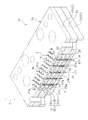
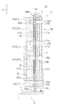
- the probe head 15 includes a plurality of probes 3, an upper guide portion 51 having an upper guide hole 51 a that holds the upper portion of the probe 3 near the proximal end portion 3 a, and a probe 3 near the distal end portion 3 b of the probe 3.
- a lower guide portion 53 having a lower guide hole 53 a for holding the lower portion, an intermediate spacer 52 disposed between the upper guide portion 51 and the lower guide portion 53, and the upper guide portion 51 and the lower guide portion 53.
- an intermediate guide portion 57 having an intermediate guide hole 57a that is accommodated in an accommodation recess 55 formed in the upper guide portion 51, the intermediate spacer 52, and the lower guide portion 53.
- the intermediate guide portion 57 includes a first intermediate guide portion 57A located on the distal end portion 3b side of the probe 3, a third intermediate guide portion 57C located on the proximal end portion 3a side of the probe 3, It is formed by including three intermediate guide portions of a second intermediate guide portion 57B located between the first intermediate guide portion 57A and the third intermediate guide portion 57C.
- a recessed portion 57b having a predetermined depth is formed in the installation range of the probe 3 on the upper surface of these three intermediate guide portions 57A, 57B, and 57C, and the lower guide portion 53 located at the bottom portion of the housing recessed portion 55 described above.
- a recess 53 b having a predetermined depth is formed from the installation range of the probe 3 on the bottom surface of the housing recess 55.
- the probe 3 described above is inserted into the upper guide hole 51a formed in the upper guide portion 51, and then a plurality of concave portions 57b formed in the three intermediate guide portions 57A, 57B, and 57C and a plurality of the recessed portions 57b are formed.
- a predetermined position where the tip portion 3b of the probe 3 protrudes from the lower surface of the probe head 15 by a predetermined length. It is comprised so that.
- the above-described three intermediate guide portions 57A, 57B, 57C are all provided with a heat dissipation structure 29, and the four springs of the aforementioned cylindrical body 17 are provided as means for providing the heat dissipation structure 29.
- Three intermediate guide portions 57A, 57B, and 57C that are arranged to face each other so as to surround the portions 31A, 31B, 31C, and 31D are formed of a high thermal conductivity material that has higher thermal conductivity than the probe 3.
- ceramics is used as the material for the intermediate guide portions 57A, 57B, and 57C.
- aluminum nitride fine ceramics having particularly high thermal conductivity can be used as an example of a suitable material.
- Use materials such as fine ceramics, machinable ceramics, resins, and polyimides (thickness, not as thin as a film) as materials for the intermediate guide portions 57A, 57B, and 57C. Can do.
- One kind of these materials or a composite structure in which a plurality of kinds are combined may be used.
- the intermediate guide portions 57A, 57B, and 57C are materials that satisfy specifications that require electrical insulation, heat dissipation, and heat resistance in addition to the thermal conductivity, and are materials that have a low coefficient of linear expansion. Preferably there is.
- the heat dissipation structure 29 may be configured by providing the probe head 35 with an aeration structure, a water cooling structure, a Peltier structure, etc., in addition to forming the intermediate guide portion 57 with a high thermal conductivity material.
- the lower guide portion 53 that holds the portion near the distal end portion 3 b of the probe 3 and the upper guide portion 51 that holds the portion near the proximal end portion 3 a of the probe 3.
- ceramic is used as an example of a high thermal conductivity material having higher thermal conductivity than the probe 3
- 42 alloy is used as an example of the material of the intermediate spacer 52.
- the guide cylinder portion 33D is pushed down to the tip portion 3b side through a part where a part of the reaction force or a joining slit 49B that becomes a joining point between the cylindrical body 17 and the second plunger 19B is formed.
- it is comprised so that the displacement of the said guide cylinder part 33A and the guide cylinder part 33D may be absorbed by the compression deformation of the four spring parts 31A, 31B, 31C, 31D.
- the current flowing from the tip 3b of the probe 3 through the first plunger 19A is as follows: guide cylinder 33A, spring 31A, guide cylinder 33B, spring 31B, gap G, spring 31C, guide cylinder 33C, spring
- the part 31D, the guide cylinder part 33D, and the first plunger 19B are transmitted in this order to reach the proximal end part 3a of the probe 3, and the electrical signal is sent to the control part 23 via the MLC 43.
- the four spring portions 31A, 31B, 31C, and 31D become high temperature due to Joule heat.
- a plurality of spring portions 31A, 31B, 31C, and 31D are arranged in a wide range of positions facing the spring portions 31A, 31B, 31C, and 31D. Since the intermediate guide portions 57A, 57B, and 57C are provided, the heat dissipation action of the intermediate guide portions 57A, 57B, and 57C is effectively exhibited, and the temperature rise of the probe 3 is suppressed. That is, the spring portions 31A, 31B, 31C, and 31D are absorbed and radiated by the inner peripheral surfaces of the intermediate guide portions 57A, 57B, and 57C of the intermediate guide portions 57A, 57C, and 57C, which are respectively opposed to each other. The rise is suppressed.
- the probe card 11 and the contact inspection apparatus 1 configured as described above, when conducting the energization inspection of the inspected object 5 using the conductive probe 3 having the spring property, Even when a current check is performed by applying a high current, an increase in temperature of the spring portion 31 provided in the cylindrical body 17 of the probe 3 can be suppressed. Thereby, since it is possible to perform an energization inspection without reducing the spring property of the probe 3, it is possible to suppress a decrease in inspection accuracy of the energization inspection.
- the probe card 11 and the contact inspection apparatus 1 according to the present invention are basically configured to have the above-described configuration, but the partial configuration may be changed or omitted without departing from the gist of the present invention. Of course, it is also possible to perform.
- the heat radiating structure 29 can be provided only for a part of the guide portions 27 in addition to being provided for all the guide portions 27 located at positions facing the probe 3.
- the heat dissipation structure 29 is applied only to a part of the guide portion 27 located at a position facing the spring portion 31.
- three intermediate guide portions 57A, 57B, and 57C are used. However, it is possible to provide four or more intermediate guide portions 57 or reduce the number of intermediate guide portions 57 to two or less.
Abstract
Description
また、第1中間ガイドフィルム105、第2中間ガイドフィルム106及び第3中間ガイドフィルム107が保持している範囲は、プローブ101のバネ作用を発現する部分108を除いた狭い範囲に設定されていた。 FIG. 9 shows the structure of a
Further, the range held by the first
しかし、従来は、通電検査の際に高電流を印加した場合に発生するジュール熱によりプローブが高温になってバネ性が低下する虞については考慮されておらず、上記特許文献1から特許文献4にもその旨の記載は何らなされていない。 In such a contact inspection apparatus, a case where a high current is applied when conducting an energization inspection has increased. When a high current is applied to the contact inspection device, a lot of Joule heat is generated and the probe becomes high temperature. And if the part which expresses the said spring property of this probe becomes high temperature, spring property will fall. Further, if the spring property is lowered, the probe cannot be pressed against the part to be inspected with an appropriate pressing force, and the inspection accuracy may be lowered.
However, conventionally, no consideration has been given to the possibility that the probe may become hot due to Joule heat generated when a high current is applied during an energization test, and the spring property may be reduced. There is no statement to that effect.
本発明の目的は、バネ性を有する導電性のプローブを使用して被検査体の通電検査を行うプローブカード及び該プローブカードを備える接触検査装置において、通電検査の際に高電流を印加した場合でもプローブのバネ性が低下する虞を低減させることにある。 Further, the first
An object of the present invention is to provide a probe card that conducts an energization inspection of an object to be inspected using a conductive probe having a spring property, and a contact inspection apparatus including the probe card, when a high current is applied during the energization inspection. However, this is to reduce the possibility that the spring property of the probe will be lowered.
ここで、前記高熱伝導性材料は、具体的にはファインセラミック系、マシナブルセラミック系、樹脂系、ポリイミド系(フィルムのような薄いものではなく、厚さをもったもの)の材料等が挙げられる。これらの材料を一種類で又は複数種類を組み合わせた複合構造で用いてもよい。
尚、当該ガイド部は、前記熱伝導性の他に、電気的絶縁性、放熱性、耐熱性の要求仕様を満たし、また線膨張係数が低い材料であることが好ましい。 The probe card according to a second aspect of the present invention is the probe card according to the first aspect, wherein at least a part of a portion of the guide portion facing the probe keeps the heat generated by the probe away from the probe. It is characterized by having a structure formed of a high thermal conductivity material that dissipates and diffuses in the direction.
Here, specific examples of the high thermal conductivity material include fine ceramic materials, machinable ceramic materials, resin materials, and polyimide materials (thickness, not as thin as a film). It is done. These materials may be used alone or in a composite structure combining a plurality of types.
In addition to the thermal conductivity, the guide portion preferably satisfies the required specifications for electrical insulation, heat dissipation, and heat resistance, and is preferably a material having a low coefficient of linear expansion.
また、本態様により当該放熱構造を構造簡単にして構築することができる。当該放熱構造は、前記高熱伝導性材料を用いる構造には限定されないことは勿論である。 According to this aspect, the heat dissipation structure is formed of a high thermal conductivity material that at least part of the portion of the guide portion facing the probe dissipates and diffuses the heat generated by the probe in a direction away from the probe. This is the configuration. With this configuration, the Joule heat can be easily absorbed and dissipated by the guide portion formed of the high thermal conductivity material while the guide portion guides the movement of the probe during the energization inspection. Thereby, the high temperature of the probe is suppressed, and the possibility that the spring property of the probe is lowered can be reduced.
Further, according to this aspect, the heat dissipation structure can be constructed with a simple structure. Of course, the heat dissipation structure is not limited to a structure using the high thermal conductivity material.
また、効果的にジュール熱を吸収することができるから、当該プローブの高温化が抑制され、プローブのバネ性が低下する虞を低減させることができる。 According to this aspect, since at least a part of the heat absorbing portion of the heat dissipation structure is located opposite to the portion that exhibits the spring property of the probe, Joule heat that is generated directly from the portion that exhibits the spring property of the probe. Therefore, it is possible to effectively suppress a decrease in the spring property of the probe.
In addition, since Joule heat can be effectively absorbed, the temperature rise of the probe can be suppressed, and the possibility that the spring property of the probe is lowered can be reduced.
本態様によれば、このような構造のプローブであっても高温化によるバネ性の低下を効果的に抑制することができる。 In the case of a probe having a structure in which the spring property of the probe is imparted by forming a slit in a part of the conductive cylinder constituting the probe and forming it in a spiral shape or the like, in particular, due to high temperature due to Joule heat There is a tendency for the springiness to decrease.
According to this aspect, even with a probe having such a structure, it is possible to effectively suppress a decrease in springiness due to a high temperature.
尚、以下の説明では、最初に図1及び図3に基づいて本発明の実施形態に係る接触検査装置の概要について説明する。次に、図2及び図4~図6に基づいて本発明の実施形態に係るプローブカードの具体的構成について説明する。更に、図7(a)(b)に基づいて当該プローブカードを使用して行う通電検査の内容をプローブの非通電時と通電時の動作を中心に説明する。 Hereinafter, a probe card and a contact inspection apparatus according to an embodiment of the present invention will be described in detail with reference to the accompanying drawings.
In the following description, first, an outline of the contact inspection apparatus according to the embodiment of the present invention will be described based on FIGS. 1 and 3. Next, a specific configuration of the probe card according to the embodiment of the present invention will be described based on FIG. 2 and FIGS. Further, the contents of the energization inspection performed using the probe card will be described with reference to FIGS. 7A and 7B, focusing on the operation when the probe is not energized and when the probe is energized.
接触検査装置1は、バネ性を有する導電性のプローブ3を被検査体5の被検査部7に対して接触させた状態で前記バネ性を利用して適切な押圧力で押圧することにより電気的な接続状態を確立する。この状態でプローブ3を通電状態にして各被検査部7の電流値や電圧差等の電気的特性を計測したり、被検査体5全体の動作試験を行って、当該被検査体5の良否を判定する目的で接触検査装置1は使用される。 (1) Outline of the contact inspection device (see FIGS. 1 and 3)
The
具体的には、接触検査装置1は、前述した被検査体5が載置される載置部9と、バネ性を有するプローブ3を備える本発明のプローブカード11と、前記載置部9上の被検査体5の被検査部7と前記プローブカード11との相対位置を接離可能に変化させる駆動部13と、を備えることによって基本的に構成されている。 Examples of the inspected
Specifically, the
また、図示の実施形態では、前述したプローブヘッド15は、図3に表すようなカード構造12に対して直接、取り付けられるように構成されている。具体的には、クランプヘッド35とスティフナー37によって支持されたプリント基板39の一例として下面に固定リング41を使用して取り付けられたMLC(Multi Level Cell)43に、対して、下方から当該プローブヘッド15を挿し込んで固定ネジ45を締め付けることによってプローブヘッド15は取り付けられるように構成されている。 The
In the illustrated embodiment, the
プローブカード11は、前述したようにバネ性を有するプローブ3と、該プローブ3を保持するプローブヘッド15と、を備えている。そして、プローブヘッド15には、プローブ3を押圧方向となる軸方向Zに移動可能に保持するガイド部27が設けられており、該ガイド部27には、通電により発生したプローブ3の熱を吸熱してプローブ3外に流す放熱構造29が備えられている。 (2) Specific configuration of the probe card (see FIG. 2 and FIGS. 4 to 6)
As described above, the
図2に表したように、プローブ3は、スリーブ状の案内筒部33の一部にバネ性を発現するバネ部31(31A、31B、31C、31D)を有する筒体17と、該筒体17に対して挿入され、前記案内筒部33の一部に接合されることによって該筒体17と一体になって軸方向Zに変位する導電性を有するプランジャー(棒状体)19と、を備えている。
また、本実施形態では、プローブ3のバネ性は、導電性を有する前記筒体17に設けられる螺旋状のスリット47によって形成されるバネ部31(31A、31B、31C、31D)によって付与されている。 (A) Specific configuration of the probe (see FIG. 5)
As shown in FIG. 2, the
In this embodiment, the spring property of the
尚、前記3ヶ所に設けられるバネ部31は一例として先端部3b寄りと基端部3a寄りに設けられている2本のバネ部31A、31Dが長く、その中央においてギャップGを隔てて設けられる2本のバネ部31B、31Cが短くなるように形成されている。また、前記ギャップGを境にして先端部3b側に配置されるバネ部31A、31Bと基端部3a側に配置されるバネ部31C、31Dの巻方向をそれぞれ逆にしており、これにより、プローブ3を押圧した時の筒体17の捩れを解消している。 The
The
また、前記バネ部31を設けるための螺旋状のスリット47の形成に当たっては、レーザー加工やエッチング処理等をそれぞれ単独で実施したり、両者を組み合わせて実施することが可能である。 Further, the
Further, in forming the spiral slit 47 for providing the
このうち、第1プランジャー19Aは、一例としてAgPdCuなどのパラジウム合金製で、前記筒体17に組み付けた状態で該筒体17の先端部3b側の端面から1mm程度、先端が突出し、一方、第1プランジャー19Aの後端は、前記案内筒部33Cの内部に到達し得る長さに形成されている。 The
Among these, the
そして、前記第1プランジャー19Aの先端がプローブ3の先端部3bとなり、通電検査時において前述した被検査体5の被検査部7に接触するように構成されている。 The
The distal end of the
また、前記第2プランジャー19Bは、前述した案内筒部33Dに形成されている接合用スリット49Bの個所で筒体17に接合され、筒体17と一体になって軸方向Zに移動し得るように構成されている。 On the other hand, the
Further, the
そして、前記第2プランジャー19Bの後端がプローブ3の基端部3aになり、前述したカード構造12のMLC43の入力側の接点に当接して、通電検査時において前述した各被検査部7の電気的特性等を出力できるように構成されている。 A gap S of about 0.4 mm is formed between the rear end of the
The rear end of the
プローブヘッド15は、本実施形態では、複数本のプローブ3と、プローブ3の基端部3a寄りの上部を保持する上部ガイド穴51aを有する上部ガイド部51と、プローブ3の先端部3b寄りの下部を保持する下部ガイド穴53aを有する下部ガイド部53と、前記上部ガイド部51と下部ガイド部53との中間に配置される中間スペーサー52と、前記上部ガイド部51と前記下部ガイド部53の間に位置し、上部ガイド部51、中間スペーサー52及び下部ガイド部53に形成された収容凹部55に収容される中間ガイド穴57aを有する中間ガイド部57と、を備えることによって構成されている。 (B) Specific configuration of the probe head (see FIGS. 2, 4 and 6)
In the present embodiment, the
また、これら3つの中間ガイド部57A、57B、57Cの上面のプローブ3の設置範囲には所定深さの凹部57bがそれぞれ形成されており、前述した収容凹部55の底部に位置する下部ガイド部53にも収容凹部55の底面のプローブ3の設置範囲から所定深さの凹部53bが形成されている。 In the present embodiment, the
In addition, a recessed
そして、本実施形態では中間ガイド部57A、57B、57Cの材料としてセラミックスを採用している。また、セラミックスの中でも特に熱伝導率の高い窒化アルミニウム系のファインセラミックスが好適な材料として一例として使用できる。中間ガイド部57A、57B、57Cの材料として、ファインセラミック系、マシナブルセラミック系、樹脂系、ポリイミド系(フィルムのような薄いものではなく、厚さをもったもの)の材料等を使用することができる。これらの材料の一種類で又は複数種類を組み合わせた複合構造で用いてもよい。
尚、当該中間ガイド部57A、57B、57Cは、前記熱伝導性の他に、電気的絶縁性、放熱性、耐熱性が要求される仕様を満たす材料であり、また線膨張係数が低い材料であることが好ましい。 Further, in the present embodiment, the above-described three
In this embodiment, ceramics is used as the material for the
The
次に、前記プローブカード11を備えた接触検査装置1を使用することによって実行される通電検査の内容をプローブ3の非通電時と通電時の動作を中心に説明する。
(A)非通電時(図7参照)
非通電時はプローブ3の先端部3bは、載置部9上に載置された被検査体5の被検査部7に対して離間した状態になっている。この状態では、バネ部31には負荷が掛かっていないため、第1プランジャー19Aの先端は筒体17の先端部3b側の端面から前述したように1mm程度突出した状態になっている。 (3) Details of the energization inspection performed using the probe card (see Figs. 7 and 8)
Next, the content of the energization inspection performed by using the
(A) When not energized (see Fig. 7)
When not energized, the
この状態から駆動部13を起動し、プローブ3の先端部3bを被検査部7に対して相対的に移動させて該被検査部7に接触させ、所定の押圧力で押し付ける。そして、プローブ3の先端部3bには被検査部7から基端部3a側に向けての反力が作用し、該反力の一部は第1プランジャー19Aと筒体17との接合点となる接合用スリット49Aが形成されている部位を介して案内筒部33Aを基端部3a側に押し上げるように作用する。
また、前記反力の一部か筒体17と第2プランジャー19Bとの接合点となる接合用スリット49Bが形成されている部位を介して案内筒部33Dを先端部3b側に押し下げるように作用する。そして、前記案内筒部33Aと案内筒部33Dの変位を4つのバネ部31A、31B、31C、31Dの圧縮変形によって吸収するように構成されている。 (B) When energized (see Fig. 8)
From this state, the
Further, the
そして、この際、前記4つのバネ部31A、31B、31C、31Dがジュール熱により高温になるが、本実施形態ではこれらのバネ部31A、31B、31C、31Dと対向する位置の広い範囲に複数の中間ガイド部57A、57B、57Cが設けられているので、これらの中間ガイド部57A、57B、57Cが有する放熱作用が効果的に発揮されて該プローブ3の温度上昇が抑制される。即ち、前記バネ部31A、31B、31C、31Dは、それぞれ対向する位置に存する中間ガイド部57A、57B、57Cの中間ガイド穴57aの内周面によって前記ジュール熱を吸収されて放熱され、その温度上昇が抑制される。 The current flowing from the
At this time, the four
本発明に係るプローブカード11及び接触検査装置1は、以上述べたような構成を有することを基本とするものであるが、本願発明の要旨を逸脱しない範囲内の部分的構成の変更や省略等を行うことも勿論可能である。 [Other embodiments]
The
また、前記実施形態では3つの中間ガイド部57A、57B、57Cを使用したが中間ガイド部57を4つ以上設けたり、中間ガイド部57を2つ以下に減らすことが可能である。 For example, the
In the embodiment, three
7…被検査部、9…載置部、11…プローブカード、12…カード構造、
13…駆動部、15…プローブヘッド、17…筒体、19…プランジャー(棒状体)、
23…制御部、25…テスター、27…ガイド部、29…放熱構造、31…バネ部、
33…案内筒部、35…クランプヘッド、37…スティフナー、39…プリント基板、
41…固定リング、43…MLC、45…固定ネジ、47…スリット、
49A、49B…接合用スリット、51…上部ガイド部、51a…上部ガイド穴、
52…中間スペーサー、53…下部ガイド部、53a…下部ガイド穴、
53b…凹部、55…収容凹部、57…中間ガイド部、57a…中間ガイド穴、
57b…凹部、Z…軸方向、G…ギャップ、S…間隙 DESCRIPTION OF
7 ... inspected part, 9 ... placing part, 11 ... probe card, 12 ... card structure,
13 ... Drive unit, 15 ... Probe head, 17 ... Tube, 19 ... Plunger (rod-like body),
23 ... Control part, 25 ... Tester, 27 ... Guide part, 29 ... Heat dissipation structure, 31 ... Spring part,
33 ... guide tube portion, 35 ... clamp head, 37 ... stiffener, 39 ... printed circuit board,
41 ... fixing ring, 43 ... MLC, 45 ... fixing screw, 47 ... slit,
49A, 49B ... Slit for bonding, 51 ... Upper guide portion, 51a ... Upper guide hole,
52 ... Intermediate spacer, 53 ... Lower guide part, 53a ... Lower guide hole,
53b ... concave portion, 55 ... accommodating concave portion, 57 ... intermediate guide portion, 57a ... intermediate guide hole,
57b ... concave portion, Z ... axial direction, G ... gap, S ... gap
Claims (8)
- バネ性を有するプローブと、
前記プローブを保持するプローブヘッドと、を備えるプローブカードであって、
前記プローブヘッドは、
前記プローブを軸方向に移動可能に保持するガイド部を備え、
前記ガイド部は、通電により発生した前記プローブ熱を吸熱して該プローブ外に流す放熱構造を備えている、ことを特徴とするプローブカード。 A probe having a spring property;
A probe card comprising a probe head for holding the probe,
The probe head is
A guide portion for holding the probe so as to be movable in the axial direction;
The probe card according to claim 1, further comprising a heat dissipation structure that absorbs the probe heat generated by energization and flows the probe heat out of the probe. - 請求項1に記載されたプローブカードにおいて、
前記放熱構造は、前記ガイド部の前記プローブと対向する部分の少なくとも一部が、前記プローブで発生した熱を該プローブから遠ざかる方向に放熱、拡散させる高熱伝導性材料で形成された構成である、ことを特徴とするプローブカード。 The probe card according to claim 1,
The heat dissipation structure is a configuration in which at least a part of the portion of the guide portion facing the probe is formed of a high thermal conductive material that dissipates and diffuses heat generated by the probe in a direction away from the probe. A probe card characterized by that. - 請求項1又は2に記載されたプローブカードにおいて、
前記放熱構造の吸熱部位の少なくとも一部は、前記プローブのバネ性を発現する部分と対向して位置する、ことを特徴とするプローブカード。 In the probe card according to claim 1 or 2,
The probe card according to claim 1, wherein at least a part of the heat absorbing portion of the heat radiating structure is positioned to face a portion expressing the spring property of the probe. - 請求項1から3のいずれか一項に記載されたプローブカードにおいて、
前記プローブヘッドは、
前記プローブの上部を保持する上部ガイド穴を有する上部ガイド部と、
前記プローブの下部を保持する下部ガイド穴を有する下部ガイド部と、
前記上部ガイド部と前記下部ガイド部の中間に位置し、
前記プローブの中間部を保持する中間ガイド穴を有する中間ガイド部と、を備え、
前記放熱構造を有するガイド部は、前記中間ガイド部である、ことを特徴とするプローブカード。 The probe card according to any one of claims 1 to 3,
The probe head is
An upper guide part having an upper guide hole for holding the upper part of the probe;
A lower guide part having a lower guide hole for holding the lower part of the probe;
Located between the upper guide part and the lower guide part,
An intermediate guide portion having an intermediate guide hole for holding the intermediate portion of the probe, and
The probe card, wherein the guide portion having the heat dissipation structure is the intermediate guide portion. - 請求項4に記載されたプローブカードにおいて、
前記放熱構造を有するガイド部は、上下方向に複数に分割されている、ことを特徴とするプローブカード。 The probe card according to claim 4, wherein
The guide card having the heat dissipation structure is divided into a plurality of parts in the vertical direction. - 請求項1から5のいずれか一項に記載されたプローブカードにおいて、
前記プローブのバネ性は、該プローブを構成する導電性の筒体に設けられたスリットによって付与されている、ことを特徴とするプローブカード。 In the probe card according to any one of claims 1 to 5,
The probe card according to claim 1, wherein the spring property of the probe is provided by a slit provided in a conductive cylinder constituting the probe. - 請求項6に記載されたプローブカードにおいて、
前記プローブは、スリーブ状の案内筒部の一部にバネ性を発現するバネ部を有する筒体と、
前記筒体に対して挿入され、前記案内筒部の一部に接合されることによって筒体と一体になって軸方向に変位する導電性を有する棒状体と、を備えている、ことを特徴とするプローブカード。 The probe card according to claim 6, wherein
The probe has a cylindrical body having a spring portion that expresses a spring property in a part of a sleeve-shaped guide cylindrical portion,
A conductive rod-like body that is inserted into the cylindrical body and is joined to a part of the guide cylinder portion so as to be integrated with the cylindrical body and displaced in the axial direction. And probe card. - 被検査体が載置される載置部と、
バネ性を有するプローブを備えるプローブカードと、
前記載置部上の被検査体の被検査部と前記プローブカードとの相対位置を接離可能に変化させる駆動部と、を備え、
前記載置部上に載置された被検査体の被検査部に対して、前記プローブが接触することによって通電検査を行う接触検査装置であって、
前記プローブカードは、請求項1から7のいずれか一項に記載されたプローブカードである、ことを特徴とする接触検査装置。 A placement section on which the object to be inspected is placed;
A probe card comprising a probe having spring properties;
A drive unit that changes the relative position of the probe card to be tested and the probe card on the placement unit in such a way that the probe card can be contacted and separated; and
A contact inspection device that conducts an electric current inspection by contacting the probe with respect to an inspection portion of an inspection object placed on the placement portion,
The contact inspection apparatus according to claim 1, wherein the probe card is the probe card according to claim 1.
Priority Applications (4)
| Application Number | Priority Date | Filing Date | Title |
|---|---|---|---|
| US15/770,062 US10775411B2 (en) | 2015-10-21 | 2016-10-13 | Probe card and contact inspection device |
| EP16857343.4A EP3367108A4 (en) | 2015-10-21 | 2016-10-13 | Probe card and contact inspection device |
| CN201680061723.XA CN108351371B (en) | 2015-10-21 | 2016-10-13 | Probe card and contact inspection apparatus |
| KR1020187011736A KR102015741B1 (en) | 2015-10-21 | 2016-10-13 | Probe card and contact inspection device |
Applications Claiming Priority (2)
| Application Number | Priority Date | Filing Date | Title |
|---|---|---|---|
| JP2015207263A JP6890921B2 (en) | 2015-10-21 | 2015-10-21 | Probe card and contact inspection device |
| JP2015-207263 | 2015-10-21 |
Publications (1)
| Publication Number | Publication Date |
|---|---|
| WO2017069028A1 true WO2017069028A1 (en) | 2017-04-27 |
Family
ID=58557432
Family Applications (1)
| Application Number | Title | Priority Date | Filing Date |
|---|---|---|---|
| PCT/JP2016/080301 WO2017069028A1 (en) | 2015-10-21 | 2016-10-13 | Probe card and contact inspection device |
Country Status (7)
| Country | Link |
|---|---|
| US (1) | US10775411B2 (en) |
| EP (1) | EP3367108A4 (en) |
| JP (1) | JP6890921B2 (en) |
| KR (1) | KR102015741B1 (en) |
| CN (1) | CN108351371B (en) |
| TW (1) | TWI627413B (en) |
| WO (1) | WO2017069028A1 (en) |
Cited By (1)
| Publication number | Priority date | Publication date | Assignee | Title |
|---|---|---|---|---|
| WO2018221234A1 (en) * | 2017-05-30 | 2018-12-06 | 株式会社日本マイクロニクス | Electrical connection apparatus |
Families Citing this family (13)
| Publication number | Priority date | Publication date | Assignee | Title |
|---|---|---|---|---|
| JP6892277B2 (en) * | 2017-02-10 | 2021-06-23 | 株式会社日本マイクロニクス | Probes and electrical connections |
| JP6980410B2 (en) * | 2017-05-23 | 2021-12-15 | 株式会社日本マイクロニクス | probe |
| US10566256B2 (en) * | 2018-01-04 | 2020-02-18 | Winway Technology Co., Ltd. | Testing method for testing wafer level chip scale packages |
| WO2020039969A1 (en) * | 2018-08-23 | 2020-02-27 | 日本電産リード株式会社 | Inspection jig, inspection device, and contact terminal |
| KR102037657B1 (en) | 2018-09-05 | 2019-10-29 | 주식회사 아이에스시 | Probe card for electrical test and probe head for probe card |
| TW202032137A (en) * | 2019-02-22 | 2020-09-01 | 日商日本電產理德股份有限公司 | Test jig |
| KR102037198B1 (en) | 2019-06-16 | 2019-10-28 | 심민섭 | Probe card inspection device |
| CN112240945A (en) * | 2019-07-17 | 2021-01-19 | 中华精测科技股份有限公司 | Improved structure of wafer probe card |
| JP7148472B2 (en) * | 2019-09-27 | 2022-10-05 | 株式会社フェローテックマテリアルテクノロジーズ | Ceramic part and method for manufacturing ceramic part |
| KR20210098090A (en) | 2020-01-31 | 2021-08-10 | (주)포인트엔지니어링 | Probe head and probe card having the same |
| JP7175518B2 (en) * | 2020-06-02 | 2022-11-21 | 東理システム株式会社 | Electrical characteristic inspection unit device for power conversion circuit devices |
| JP2022116470A (en) * | 2021-01-29 | 2022-08-10 | 株式会社村田製作所 | Probe device |
| KR20230127485A (en) * | 2022-02-25 | 2023-09-01 | (주)티에스이 | Lower Friction Probe Head |
Citations (9)
| Publication number | Priority date | Publication date | Assignee | Title |
|---|---|---|---|---|
| JPH06163657A (en) * | 1992-11-27 | 1994-06-10 | Nec Corp | Probe card |
| JP2003215163A (en) * | 2002-01-24 | 2003-07-30 | Japan Electronic Materials Corp | Probe card |
| JP2007012475A (en) * | 2005-06-30 | 2007-01-18 | Fujitsu Ltd | Socket and electronic equipment |
| JP2009230897A (en) * | 2008-03-19 | 2009-10-08 | Fujitsu Ltd | Electronic component jointing device, electronic unit, and electronic device |
| WO2011115082A1 (en) * | 2010-03-15 | 2011-09-22 | 日本電産リード株式会社 | Connection terminal and connection jig |
| WO2013051675A1 (en) * | 2011-10-07 | 2013-04-11 | 日本発條株式会社 | Probe unit |
| WO2013051099A1 (en) * | 2011-10-04 | 2013-04-11 | 富士通株式会社 | Testing jig and semiconductor device test method |
| WO2014021194A1 (en) * | 2012-08-01 | 2014-02-06 | 日本電子材料株式会社 | Guide plate for probe guard and probe guard provided with same |
| JP2014181910A (en) * | 2013-03-18 | 2014-09-29 | Japan Electronic Materials Corp | Guide plate for probe card |
Family Cites Families (18)
| Publication number | Priority date | Publication date | Assignee | Title |
|---|---|---|---|---|
| JP4455940B2 (en) | 2004-06-17 | 2010-04-21 | 株式会社日本マイクロニクス | Electrical connection device |
| JP2007057444A (en) * | 2005-08-25 | 2007-03-08 | Nidec-Read Corp | Board inspection device and temperature maintenance mechanism for same |
| US7601009B2 (en) | 2006-05-18 | 2009-10-13 | Centipede Systems, Inc. | Socket for an electronic device |
| JP2008243861A (en) * | 2007-03-23 | 2008-10-09 | Tokyo Electron Ltd | Inspection apparatus and method |
| JP2009162483A (en) | 2007-12-28 | 2009-07-23 | Micronics Japan Co Ltd | Electrical connection device |
| JP2009276215A (en) * | 2008-05-15 | 2009-11-26 | Tokyo Electron Ltd | Probe apparatus and method for correcting contact position |
| JP5222038B2 (en) * | 2008-06-20 | 2013-06-26 | 東京エレクトロン株式会社 | Probe device |
| CN201293798Y (en) * | 2008-10-31 | 2009-08-19 | 中茂电子(深圳)有限公司 | Probe card for solar battery detection bench |
| JP5826466B2 (en) * | 2010-06-25 | 2015-12-02 | 東京エレクトロン株式会社 | Probe card parallel adjustment mechanism and inspection device |
| WO2012039226A1 (en) * | 2010-09-21 | 2012-03-29 | Nishikawa Hideo | Inspecting jig and contact |
| JP6092509B2 (en) * | 2011-10-17 | 2017-03-08 | 東京エレクトロン株式会社 | Contact terminal support and probe card |
| JP2014025737A (en) * | 2012-07-25 | 2014-02-06 | Nidec-Read Corp | Inspecting tool and contact |
| JP6017228B2 (en) | 2012-08-27 | 2016-10-26 | 株式会社日本マイクロニクス | Electrical connection device |
| JP2014048266A (en) * | 2012-09-04 | 2014-03-17 | Toshiba Corp | Probe card, and test method and test device of imaging device using the same |
| TWI548879B (en) * | 2014-01-28 | 2016-09-11 | Spring sleeve probe | |
| JP6546719B2 (en) | 2014-02-07 | 2019-07-17 | 株式会社日本マイクロニクス | Contact inspection device |
| TW201533449A (en) * | 2014-02-24 | 2015-09-01 | Mpi Corp | Probing device with spring-barrel probe |
| TWI570415B (en) * | 2015-10-02 | 2017-02-11 | A spring probe having an outer sleeve and a probe device having the spring probe |
-
2015
- 2015-10-21 JP JP2015207263A patent/JP6890921B2/en active Active
-
2016
- 2016-10-13 KR KR1020187011736A patent/KR102015741B1/en active IP Right Grant
- 2016-10-13 WO PCT/JP2016/080301 patent/WO2017069028A1/en active Application Filing
- 2016-10-13 EP EP16857343.4A patent/EP3367108A4/en active Pending
- 2016-10-13 US US15/770,062 patent/US10775411B2/en active Active
- 2016-10-13 CN CN201680061723.XA patent/CN108351371B/en active Active
- 2016-10-18 TW TW105133572A patent/TWI627413B/en active
Patent Citations (9)
| Publication number | Priority date | Publication date | Assignee | Title |
|---|---|---|---|---|
| JPH06163657A (en) * | 1992-11-27 | 1994-06-10 | Nec Corp | Probe card |
| JP2003215163A (en) * | 2002-01-24 | 2003-07-30 | Japan Electronic Materials Corp | Probe card |
| JP2007012475A (en) * | 2005-06-30 | 2007-01-18 | Fujitsu Ltd | Socket and electronic equipment |
| JP2009230897A (en) * | 2008-03-19 | 2009-10-08 | Fujitsu Ltd | Electronic component jointing device, electronic unit, and electronic device |
| WO2011115082A1 (en) * | 2010-03-15 | 2011-09-22 | 日本電産リード株式会社 | Connection terminal and connection jig |
| WO2013051099A1 (en) * | 2011-10-04 | 2013-04-11 | 富士通株式会社 | Testing jig and semiconductor device test method |
| WO2013051675A1 (en) * | 2011-10-07 | 2013-04-11 | 日本発條株式会社 | Probe unit |
| WO2014021194A1 (en) * | 2012-08-01 | 2014-02-06 | 日本電子材料株式会社 | Guide plate for probe guard and probe guard provided with same |
| JP2014181910A (en) * | 2013-03-18 | 2014-09-29 | Japan Electronic Materials Corp | Guide plate for probe card |
Cited By (4)
| Publication number | Priority date | Publication date | Assignee | Title |
|---|---|---|---|---|
| WO2018221234A1 (en) * | 2017-05-30 | 2018-12-06 | 株式会社日本マイクロニクス | Electrical connection apparatus |
| JP2018200289A (en) * | 2017-05-30 | 2018-12-20 | 株式会社日本マイクロニクス | Electric connection device |
| US11150268B2 (en) | 2017-05-30 | 2021-10-19 | Kabushiki Kaisha Nihon Micronics | Electric connection device |
| JP7075725B2 (en) | 2017-05-30 | 2022-05-26 | 株式会社日本マイクロニクス | Electrical connection device |
Also Published As
| Publication number | Publication date |
|---|---|
| KR102015741B1 (en) | 2019-08-28 |
| TW201728908A (en) | 2017-08-16 |
| EP3367108A4 (en) | 2019-06-19 |
| US10775411B2 (en) | 2020-09-15 |
| TWI627413B (en) | 2018-06-21 |
| CN108351371A (en) | 2018-07-31 |
| JP2017078660A (en) | 2017-04-27 |
| KR20180059867A (en) | 2018-06-05 |
| EP3367108A1 (en) | 2018-08-29 |
| JP6890921B2 (en) | 2021-06-18 |
| CN108351371B (en) | 2021-04-27 |
| US20180299489A1 (en) | 2018-10-18 |
Similar Documents
| Publication | Publication Date | Title |
|---|---|---|
| WO2017069028A1 (en) | Probe card and contact inspection device | |
| US7262613B2 (en) | Inspection method and inspection apparatus for inspecting electrical characteristics of inspection object | |
| US9733299B2 (en) | Inspection jig | |
| US8816710B2 (en) | Inspection contact element and inspecting jig | |
| US6967492B2 (en) | Spring contact probe device for electrical testing | |
| JP4041831B2 (en) | Substrate inspection jig and electrode structure of connection electrode portion in this jig | |
| US20170045552A1 (en) | Probe | |
| JP6209376B2 (en) | Electrical connection device | |
| JP6209375B2 (en) | Electrical connection device | |
| JP2010060316A (en) | Anisotropic conductive member and measuring substrate having anisotropic conductivity | |
| KR102498454B1 (en) | Contact probe and inspection jig | |
| US7148713B1 (en) | Algoristic spring as probe | |
| JP2010078432A (en) | Substrate inspection jig and contactor | |
| WO2016043327A1 (en) | Probe unit | |
| JP2007024702A (en) | Semiconductor inspection socket equipped with heater mechanism | |
| TWI646333B (en) | Probe and electrical connection device | |
| JP2008267833A (en) | Jig for inspecting substrate and structure for electrode of connecting electrode in the jig | |
| JP2019039756A (en) | probe | |
| JP2007273580A (en) | Semiconductor device evaluator and evaluation method | |
| JP2013253785A (en) | Probe card | |
| JP2010091314A (en) | Board inspection tool and inspection probe | |
| KR20140105897A (en) | Probe card and apparatus for testing an object including the same | |
| JP5290820B2 (en) | Electronic component measuring apparatus and measuring method | |
| JP2005114547A (en) | Contact probe and contact apparatus using the probe | |
| JP6961422B2 (en) | probe |
Legal Events
| Date | Code | Title | Description |
|---|---|---|---|
| 121 | Ep: the epo has been informed by wipo that ep was designated in this application |
Ref document number: 16857343 Country of ref document: EP Kind code of ref document: A1 |
|
| WWE | Wipo information: entry into national phase |
Ref document number: 15770062 Country of ref document: US |
|
| NENP | Non-entry into the national phase |
Ref country code: DE |
|
| ENP | Entry into the national phase |
Ref document number: 20187011736 Country of ref document: KR Kind code of ref document: A |
|
| WWE | Wipo information: entry into national phase |
Ref document number: 2016857343 Country of ref document: EP |