JP2017009449A - Contact probe type temperature detector, evaluation device of semiconductor device and evaluation method of semiconductor device - Google Patents

Contact probe type temperature detector, evaluation device of semiconductor device and evaluation method of semiconductor device Download PDF

Info

Publication number
JP2017009449A
JP2017009449A JP2015125432A JP2015125432A JP2017009449A JP 2017009449 A JP2017009449 A JP 2017009449A JP 2015125432 A JP2015125432 A JP 2015125432A JP 2015125432 A JP2015125432 A JP 2015125432A JP 2017009449 A JP2017009449 A JP 2017009449A
Authority
JP
Japan
Prior art keywords
semiconductor device
evaluation
temperature
measured
temperature detector
Prior art date
Legal status (The legal status is an assumption and is not a legal conclusion. Google has not performed a legal analysis and makes no representation as to the accuracy of the status listed.)
Pending
Application number
JP2015125432A
Other languages
Japanese (ja)
Inventor
欽也 山下
Kinya Yamashita
欽也 山下
貴也 野口
Takaya Noguchi
貴也 野口
岡田 章
Akira Okada
章 岡田
肇 秋山
Hajime Akiyama
肇 秋山
和起 上野
Kazuki Ueno
和起 上野
Current Assignee (The listed assignees may be inaccurate. Google has not performed a legal analysis and makes no representation or warranty as to the accuracy of the list.)
Mitsubishi Electric Corp
Original Assignee
Mitsubishi Electric Corp
Priority date (The priority date is an assumption and is not a legal conclusion. Google has not performed a legal analysis and makes no representation as to the accuracy of the date listed.)
Filing date
Publication date
Application filed by Mitsubishi Electric Corp filed Critical Mitsubishi Electric Corp
Priority to JP2015125432A priority Critical patent/JP2017009449A/en
Priority to US15/064,054 priority patent/US20160377486A1/en
Priority to CN201610466367.1A priority patent/CN106291302A/en
Publication of JP2017009449A publication Critical patent/JP2017009449A/en
Pending legal-status Critical Current

Links

Images

Classifications

    • GPHYSICS
    • G01MEASURING; TESTING
    • G01KMEASURING TEMPERATURE; MEASURING QUANTITY OF HEAT; THERMALLY-SENSITIVE ELEMENTS NOT OTHERWISE PROVIDED FOR
    • G01K1/00Details of thermometers not specially adapted for particular types of thermometer
    • G01K1/14Supports; Fastening devices; Arrangements for mounting thermometers in particular locations
    • G01K1/143Supports; Fastening devices; Arrangements for mounting thermometers in particular locations for measuring surface temperatures
    • GPHYSICS
    • G01MEASURING; TESTING
    • G01RMEASURING ELECTRIC VARIABLES; MEASURING MAGNETIC VARIABLES
    • G01R31/00Arrangements for testing electric properties; Arrangements for locating electric faults; Arrangements for electrical testing characterised by what is being tested not provided for elsewhere
    • G01R31/26Testing of individual semiconductor devices
    • G01R31/2601Apparatus or methods therefor
    • GPHYSICS
    • G01MEASURING; TESTING
    • G01KMEASURING TEMPERATURE; MEASURING QUANTITY OF HEAT; THERMALLY-SENSITIVE ELEMENTS NOT OTHERWISE PROVIDED FOR
    • G01K7/00Measuring temperature based on the use of electric or magnetic elements directly sensitive to heat ; Power supply therefor, e.g. using thermoelectric elements
    • G01K7/02Measuring temperature based on the use of electric or magnetic elements directly sensitive to heat ; Power supply therefor, e.g. using thermoelectric elements using thermoelectric elements, e.g. thermocouples
    • GPHYSICS
    • G01MEASURING; TESTING
    • G01KMEASURING TEMPERATURE; MEASURING QUANTITY OF HEAT; THERMALLY-SENSITIVE ELEMENTS NOT OTHERWISE PROVIDED FOR
    • G01K7/00Measuring temperature based on the use of electric or magnetic elements directly sensitive to heat ; Power supply therefor, e.g. using thermoelectric elements
    • G01K7/16Measuring temperature based on the use of electric or magnetic elements directly sensitive to heat ; Power supply therefor, e.g. using thermoelectric elements using resistive elements
    • G01K7/18Measuring temperature based on the use of electric or magnetic elements directly sensitive to heat ; Power supply therefor, e.g. using thermoelectric elements using resistive elements the element being a linear resistance, e.g. platinum resistance thermometer
    • GPHYSICS
    • G01MEASURING; TESTING
    • G01KMEASURING TEMPERATURE; MEASURING QUANTITY OF HEAT; THERMALLY-SENSITIVE ELEMENTS NOT OTHERWISE PROVIDED FOR
    • G01K7/00Measuring temperature based on the use of electric or magnetic elements directly sensitive to heat ; Power supply therefor, e.g. using thermoelectric elements
    • G01K7/16Measuring temperature based on the use of electric or magnetic elements directly sensitive to heat ; Power supply therefor, e.g. using thermoelectric elements using resistive elements
    • G01K7/22Measuring temperature based on the use of electric or magnetic elements directly sensitive to heat ; Power supply therefor, e.g. using thermoelectric elements using resistive elements the element being a non-linear resistance, e.g. thermistor
    • HELECTRICITY
    • H01ELECTRIC ELEMENTS
    • H01CRESISTORS
    • H01C7/00Non-adjustable resistors formed as one or more layers or coatings; Non-adjustable resistors made from powdered conducting material or powdered semi-conducting material with or without insulating material
    • H01C7/008Thermistors

Abstract

PROBLEM TO BE SOLVED: To provide a technology capable of suppressing aerial discharge when evaluating electrical characteristic of a semiconductor device, and precisely detecting temperature of the semiconductor device.SOLUTION: A probe 7 for detecting temperature which is a contact probe type temperature detector includes a plunger part 12 capable of contacting a semiconductor device 5 which is to be measured, a spring member 17 arranged at a base end part of the plunger part 12, a barrel part 14 which pressurizes the plunger part 12 to the semiconductor device 5 side through the spring member 17, and a thermocouple 19 which is a temperature measuring part for detecting temperature of the semiconductor device 5.SELECTED DRAWING: Figure 5

Description

本発明は、半導体装置の電気的特性を評価する際に半導体装置の温度を検出する技術に関するものである。   The present invention relates to a technique for detecting the temperature of a semiconductor device when evaluating the electrical characteristics of the semiconductor device.

被測定物である半導体装置の電気的特性を評価する際、半導体装置の温度を精度よく検出することは重要である。特に温度特性の評価において、評価時の温度検出が不安定であれば、温度特性そのものに誤差が含まれることになる。また、電気的特性を評価する際、大電流かつ高電圧印加によって半導体装置の温度が変化することがある。その場合も電気的特性とともに、半導体装置の温度変化を検出することは重要である。   When evaluating the electrical characteristics of a semiconductor device, which is an object to be measured, it is important to accurately detect the temperature of the semiconductor device. In particular, in temperature characteristic evaluation, if temperature detection at the time of evaluation is unstable, an error is included in the temperature characteristic itself. Further, when evaluating electrical characteristics, the temperature of the semiconductor device may change due to application of a large current and a high voltage. In that case as well, it is important to detect the temperature change of the semiconductor device along with the electrical characteristics.

このような状況の下、半導体装置の温度検出方法として、非接触式の手法が知られている。例えば、非接触式としては、光学式の放射温度計による温度検出があるが、半導体装置の表面が鏡面であれば、温度検出は困難である。検出できたとしても、放射率の設定次第で検出温度は容易に変化するため、半導体装置の温度を正確に形成するものではない。   Under such circumstances, a non-contact method is known as a temperature detection method for a semiconductor device. For example, as the non-contact type, there is temperature detection by an optical radiation thermometer, but if the surface of the semiconductor device is a mirror surface, temperature detection is difficult. Even if it can be detected, the temperature of the semiconductor device is not accurately formed because the detection temperature easily changes depending on the setting of the emissivity.

被測定物の温度の検出方法として、例えば特許文献1,2には以下のような方法が開示されている。特許文献1には、被測定物を設置する樹脂製の設置台に温度センサが設置され、この温度センサで計測された温度に基づいて槽内の温度が制御されることが開示されている。また、特許文献2には、パワーモジュール内にリード付サーミスタが設けられ、そのサーミスタによって半導体素子の温度が計測されることが開示されている。   As a method for detecting the temperature of the object to be measured, for example, Patent Documents 1 and 2 disclose the following methods. Patent Document 1 discloses that a temperature sensor is installed on a resin-made installation table on which an object to be measured is installed, and the temperature in the tank is controlled based on the temperature measured by the temperature sensor. Patent Document 2 discloses that a thermistor with leads is provided in the power module, and the temperature of the semiconductor element is measured by the thermistor.

また、被測定物の温度の別の検出方法として、例えば特許文献3から特許文献5に、カンチレバー方式による測定システムが開示されている。   As another method for detecting the temperature of an object to be measured, for example, Patent Document 3 to Patent Document 5 disclose a measurement system using a cantilever method.

特開2010−26715号公報JP 2010-26715 A 特開2013−254873号公報JP 2013-254873 A 特開昭61−187245号公報JP-A 61-187245 特開2007−227444号公報JP 2007-227444 A 特開2011−215007号公報JP 2011-215007 A

しかしながら、特許文献1に記載の温度センサは、樹脂からなる設置台に設置されており、かつ被測定物から離れている。このため、被測定物そのものの温度を精度よく検出することができない。また、当該温度センサは従来の評価装置に採用できるものでもなかった。   However, the temperature sensor described in Patent Document 1 is installed on an installation table made of resin and is away from the object to be measured. For this reason, it is impossible to accurately detect the temperature of the object to be measured. Moreover, the said temperature sensor was not what can be employ | adopted as the conventional evaluation apparatus.

また、特許文献2に記載のサーミスタは、空気層を介して半導体素子の温度を計測している。このため、半導体素子そのものの温度を精度よく検出することができない。   Further, the thermistor described in Patent Document 2 measures the temperature of the semiconductor element through an air layer. For this reason, the temperature of the semiconductor element itself cannot be accurately detected.

さらに、特許文献3から特許文献5に記載のカンチレバー方式による測定システムは、カンチレバー方式の原理からプローブを傾斜させる必要があり、高電圧デバイスの電気的特性を測定する場合、プローブの傾斜部分と被測定物との間の距離を任意に設定できないことから気中放電を抑制することは難しいという問題がある。   Further, the cantilever type measurement systems described in Patent Document 3 to Patent Document 5 require that the probe be tilted from the principle of the cantilever method, and when measuring the electrical characteristics of a high-voltage device, the tilted portion of the probe and the object to be covered are measured. There is a problem that it is difficult to suppress air discharge because the distance to the measurement object cannot be set arbitrarily.

そこで、本発明は、半導体装置の電気的特性を評価する際に気中放電を抑制し、かつ、半導体装置の温度を精度よく検出することが可能な技術を提供することを目的とする。   Accordingly, an object of the present invention is to provide a technique capable of suppressing air discharge when evaluating the electrical characteristics of a semiconductor device and detecting the temperature of the semiconductor device with high accuracy.

本発明に係るコンタクトプローブ型温度検出器は、被測定物と接触可能なプランジャ部と、前記プランジャ部の基端部に配置されるバネ部材と、前記バネ部材を介して前記プランジャ部を前記被測定物側に押圧するバレル部と、前記被測定物の温度を検出する測温部とを備えるものである。   A contact probe type temperature detector according to the present invention includes a plunger that can contact an object to be measured, a spring member disposed at a proximal end of the plunger, and the plunger through the spring member. A barrel portion that is pressed toward the object to be measured and a temperature measuring unit that detects the temperature of the object to be measured are provided.

本発明に係る半導体装置の評価装置は、コンタクトプローブ型温度検出器と、前記被測定物を固定するためのステージと、スプリング方式の評価用プローブと、前記評価用プローブを介して前記被測定物の電気的特性を評価する評価部とを備えるものである。   A semiconductor device evaluation apparatus according to the present invention includes a contact probe type temperature detector, a stage for fixing the measurement object, a spring-type evaluation probe, and the measurement object via the evaluation probe. And an evaluation unit for evaluating the electrical characteristics of the device.

本発明に係る半導体装置の評価方法は、半導体装置の評価装置を用いた半導体装置の評価方法であって、前記評価用プローブおよび前記評価部を用いて前記被測定物の電気的特性を評価する工程(a)と、前記コンタクトプローブ型温度検出器を用いて、前記工程(a)による評価前および前記工程(a)による評価時における前記被測定物の表面の温度を検出する工程(b)とを備えるものである。   A semiconductor device evaluation method according to the present invention is a semiconductor device evaluation method using a semiconductor device evaluation device, and evaluates electrical characteristics of the object to be measured using the evaluation probe and the evaluation unit. Step (a) and step (b) of detecting the temperature of the surface of the object to be measured before the evaluation by the step (a) and at the time of the evaluation by the step (a) by using the contact probe type temperature detector. Are provided.

本発明によれば、バレル部によってバネ部材を介してプランジャ部を被測定物側に押圧することでプランジャ部と被測定物との接触を確実なものとし、測温部で被測定物の温度を検出する。したがって、半導体装置の電気的特性を評価する際に、半導体装置の温度を精度よく検出することができる。   According to the present invention, the plunger portion is pressed toward the object to be measured by the barrel portion via the spring member, thereby ensuring contact between the plunger portion and the object to be measured. Is detected. Therefore, the temperature of the semiconductor device can be accurately detected when evaluating the electrical characteristics of the semiconductor device.

また、コンタクトプローブ型温度検出器は、バネ部材を介してプランジャ部を被測定物側に押圧する構成のため、カンチレバー方式の場合よりも被測定物からコンタクトプローブ型温度検出器の取り付け部までの距離を離すことができ、気中放電を抑制できる。   In addition, the contact probe type temperature detector is configured to press the plunger portion toward the object to be measured via a spring member, and therefore, from the object to be measured to the attachment part of the contact probe type temperature detector than in the case of the cantilever method. The distance can be increased and air discharge can be suppressed.

実施の形態に係る半導体装置の評価装置の概略図である。It is the schematic of the evaluation apparatus of the semiconductor device which concerns on embodiment. スプリング方式の評価用プローブの動作説明図である。It is operation | movement explanatory drawing of the spring type probe for evaluation. 気中放電の抑制を説明するための概略図である。It is the schematic for demonstrating suppression of an air discharge. 温度検出用プローブの概略図である。It is the schematic of the probe for temperature detection. プランジャ部の一部の概略断面図である。It is a schematic sectional drawing of a part of plunger part. 実施の形態の変形例1に係る温度検出用プローブのプランジャ部の一部の概略断面図である。It is a schematic sectional drawing of a part of plunger part of the probe for temperature detection which concerns on the modification 1 of embodiment. 実施の形態の変形例2に係る温度検出用プローブのプランジャ部の一部の概略断面図である。It is a schematic sectional drawing of a part of plunger part of the probe for temperature detection which concerns on the modification 2 of embodiment. 測温部設置治具の概略斜視図である。It is a schematic perspective view of a temperature measuring part installation jig. 実施の形態の変形例3に係る温度検出用プローブのプランジャ部の一部の概略断面図である。It is a schematic sectional drawing of a part of plunger part of the probe for temperature detection concerning the modification 3 of embodiment. 温度検出用プローブの配置構成の一例を示す概略図である。It is the schematic which shows an example of the arrangement configuration of the probe for temperature detection. 温度検出用プローブの配置構成の他の例を示す概略図である。It is the schematic which shows the other example of arrangement structure of the probe for temperature detection. 温度検出用プローブの配置構成の他の例を示す概略図である。It is the schematic which shows the other example of arrangement structure of the probe for temperature detection. 温度検出用プローブの配置構成の他の例を示す概略図である。It is the schematic which shows the other example of arrangement structure of the probe for temperature detection.

<実施の形態>
本発明の実施の形態について、図面を用いて以下に説明する。図1は、実施の形態に係る半導体装置の評価装置1の概略図である。
<Embodiment>
Embodiments of the present invention will be described below with reference to the drawings. FIG. 1 is a schematic diagram of a semiconductor device evaluation apparatus 1 according to an embodiment.

本実施の形態では、絶縁板16にスプリング方式の温度検出用プローブ7を配置して、被測定物である半導体装置5の表面の温度を、半導体装置5の電気的特性の評価前および評価時に検出する例を示す。なお、本実施の形態では、半導体装置5の縦方向、つまり面外方向に大きな電流を流す縦型構造の半導体装置5を一例として示すが、これに限るものではなく、半導体装置の一面において入出力を行う、横型構造の半導体装置であってもよい。   In the present embodiment, a spring-type temperature detection probe 7 is arranged on the insulating plate 16 so that the temperature of the surface of the semiconductor device 5 that is the object to be measured is measured before and during the evaluation of the electrical characteristics of the semiconductor device 5. An example of detection will be shown. In the present embodiment, the semiconductor device 5 having a vertical structure in which a large current flows in the vertical direction of the semiconductor device 5, that is, the out-of-plane direction is shown as an example. However, the present invention is not limited to this. It may be a lateral type semiconductor device that performs output.

評価装置1は、チャックステージ3(ステージ)、スプリング方式の評価用プローブ10、温度検出用プローブ7(コンタクトプローブ型温度検出器)、および制御部4を備えている。縦型構造の半導体装置5の評価の際、外部と接続するための一方の電極は、半導体装置5の上面に設けた接続パッド18(図2参照)と接触する評価用プローブ10となる。他方の電極は、半導体装置5の下面、つまり、半導体装置5の設置面と接触するチャックステージ3の表面となる。評価用プローブ10は、絶縁板16に固定されており、絶縁板16に接続部8aを介して接続された信号線6aを通じて、制御部4と電気的に接続されている。チャックステージ3の表面は、チャックステージ3の側面に設けた接続部8bを介して接続された信号線6bを通じて、制御部4と電気的に接続されている。   The evaluation apparatus 1 includes a chuck stage 3 (stage), a spring-type evaluation probe 10, a temperature detection probe 7 (contact probe type temperature detector), and a control unit 4. In the evaluation of the semiconductor device 5 having the vertical structure, one electrode for connection to the outside serves as the evaluation probe 10 in contact with the connection pad 18 (see FIG. 2) provided on the upper surface of the semiconductor device 5. The other electrode is the lower surface of the semiconductor device 5, that is, the surface of the chuck stage 3 that is in contact with the installation surface of the semiconductor device 5. The evaluation probe 10 is fixed to the insulating plate 16 and is electrically connected to the control unit 4 through a signal line 6a connected to the insulating plate 16 via a connecting portion 8a. The surface of the chuck stage 3 is electrically connected to the control unit 4 through a signal line 6 b connected through a connection unit 8 b provided on the side surface of the chuck stage 3.

制御部4は、評価装置1の各部を制御する。制御部4は、処理回路で構成され、処理回路は、専用のハードウェアであっても、メモリに格納されるプログラムを実行するCPU(Central Processing Unit、中央処理装置、処理装置、演算装置、マイクロプロセッサ、マイクロコンピュータ、プロセッサ、DSPともいう)であってもよい。   The control unit 4 controls each unit of the evaluation device 1. The control unit 4 is configured by a processing circuit. Even if the processing circuit is dedicated hardware, a CPU (Central Processing Unit, a central processing unit, a processing unit, an arithmetic unit, a micro unit that executes a program stored in a memory is used. A processor, a microcomputer, a processor, and a DSP).

なお、評価用プローブ10は、半導体装置5に大電流(例えば5A以上)を印加することを想定して複数個配置されている。その場合、各評価用プローブ10に加わる電流密度が略一致するように、信号線6aと絶縁板16との接続位置である接続部8aと、チャックステージ3の側面に設けた接続部8bの距離が、どの評価用プローブ10を介しても略一致する位置に各接続部8a,8bを設けることが望ましい。つまり、評価用プローブ10を介して、接続部8aと接続部8bが対向する位置にあることが望ましい。また、各評価用プローブ10と接続部8aとの間は、図示していないが、例えば絶縁板16上に設けた金属板等の配線によって接続されている。   Note that a plurality of evaluation probes 10 are arranged on the assumption that a large current (for example, 5 A or more) is applied to the semiconductor device 5. In that case, the distance between the connection portion 8a, which is the connection position between the signal line 6a and the insulating plate 16, and the connection portion 8b provided on the side surface of the chuck stage 3 so that the current densities applied to the evaluation probes 10 are substantially the same. However, it is desirable to provide each of the connection portions 8a and 8b at a position that substantially matches through any evaluation probe 10. In other words, it is desirable that the connecting portion 8a and the connecting portion 8b are in a position facing each other via the evaluation probe 10. Further, although not shown, each evaluation probe 10 and the connection portion 8a are connected by wiring such as a metal plate provided on the insulating plate 16, for example.

評価用プローブ10、温度検出用プローブ7、絶縁板16、接続部8a、および各プローブ7,10と接続部8aとを接続する配線(図示省略)にて構成されるプローブ基体2は、移動アーム9によって保持され任意の方向へ移動可能となっている。ここでは、1つの移動アーム9でのみ保持する構成としたが、これに限るものではなく、複数の移動アームにて一層安定的に保持してもよい。また、プローブ基体2を移動するのではなく、半導体装置5、つまり、チャックステージ3を移動させてもよい。   The probe base 2 constituted by the evaluation probe 10, the temperature detection probe 7, the insulating plate 16, the connection portion 8a, and the wiring (not shown) for connecting the probes 7 and 10 to the connection portion 8a includes a moving arm. 9 and is movable in any direction. Here, the structure is such that only one moving arm 9 is used for holding, but the present invention is not limited to this, and a plurality of moving arms may be used for more stable holding. Further, instead of moving the probe base 2, the semiconductor device 5, that is, the chuck stage 3 may be moved.

チャックステージ3は、半導体装置5の設置面と接触して固定するための台座であり、固定手段として、例えば真空吸着の機能を有する。なお、半導体装置5の固定手段は真空吸着に限るものではなく、静電吸着等であっても構わない。   The chuck stage 3 is a pedestal for contacting and fixing the mounting surface of the semiconductor device 5, and has, for example, a vacuum suction function as a fixing means. The fixing means for the semiconductor device 5 is not limited to vacuum suction, and may be electrostatic suction or the like.

次に、評価用プローブ10について説明する。スプリング方式の評価用プローブ10の動作説明図であり、図2(a)は、初期状態を示し、図2(b)は、接触状態を示し、図2(c)は、押圧状態を示す。   Next, the evaluation probe 10 will be described. FIG. 2A shows an initial state, FIG. 2B shows a contact state, and FIG. 2C shows a pressed state.

評価用プローブ10は、基台として機能し、絶縁板16に固定されるバレル部14、半導体装置5の表面に設けられた接続パッド18と機械的かつ電気的に接触するコンタクト部11、バレル部14の内部に組み込まれたスプリング等のバネ部材を介して接触時に摺動が可能な押し込み部13を有するプランジャ部12、およびプランジャ部12と電気的に通じて外部への出力端となる端子部15を備えている。   The evaluation probe 10 functions as a base, a barrel portion 14 fixed to the insulating plate 16, a contact portion 11 that makes mechanical and electrical contact with a connection pad 18 provided on the surface of the semiconductor device 5, and a barrel portion. A plunger portion 12 having a push-in portion 13 that can be slid at the time of contact via a spring member such as a spring incorporated in the inside of the device 14, and a terminal portion that electrically communicates with the plunger portion 12 and serves as an output end to the outside. 15 is provided.

評価用プローブ10は導電性を有する、例えば銅、タングステンまたはレニウムタングステンなどの金属材料を用いて作製されるがこれらに限るものではなく、特にコンタクト部11は導電性向上および耐久性向上等の観点から、上記の金属材料に別の部材、例えば金、パラジウム、タンタルまたはプラチナ等を被覆した材料を用いて作製されてもよい。   The evaluation probe 10 is made of a conductive metal material such as copper, tungsten, or rhenium tungsten, but is not limited thereto. In particular, the contact portion 11 has a viewpoint of improving conductivity and durability. From the above, the metal material may be manufactured using another member, for example, a material coated with gold, palladium, tantalum, platinum, or the like.

評価用プローブ10は、図2(a)に示す初期状態から、下方(−Z方向)に半導体装置5に設けた接続パッド18に向けて下降すると、図2(b)に示すように、先ず、接続パッド18とコンタクト部11が接触する。その後、評価用プローブ10は、さらに下降すると、図2(c)に示すように、押し込み部13の一部がバレル部14内にバネ部材を介して押し込まれ、半導体装置5の接続パッド18との接触を確実なものにする。   When the evaluation probe 10 is lowered from the initial state shown in FIG. 2A toward the connection pad 18 provided in the semiconductor device 5 downward (−Z direction), first, as shown in FIG. The connection pad 18 and the contact portion 11 are in contact with each other. Thereafter, when the evaluation probe 10 is further lowered, as shown in FIG. 2C, a part of the pushing portion 13 is pushed into the barrel portion 14 via a spring member, and the connection pads 18 of the semiconductor device 5 are connected. Ensure contact with

ここでは、評価用プローブ10はZ軸方向に摺動性を備えたバネ部材をその内部に設けた構成について説明したが、これに限るものではなく、例えば、後述する図4に示すスプリング方式の温度検出用プローブ7のように、バネ部材を外部に設けた構成であっても構わない。   Here, the configuration has been described in which the evaluation probe 10 is provided with a spring member having slidability in the Z-axis direction. However, the present invention is not limited to this, and for example, a spring-type spring shown in FIG. A configuration in which a spring member is provided outside as in the temperature detection probe 7 may be employed.

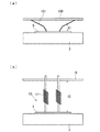
次に、評価用プローブ10および温度検出用プローブ7においてスプリング方式を用いるメリットについて前提技術と対比しながら説明する。図3は、気中放電の抑制を説明するための概略図であり、図3(a)は、前提技術であるカンチレバー方式の場合の例である。図3(b)は、スプリング方式の場合の例であり、例として評価用プローブ10を示す図である。   Next, the merit of using the spring method in the evaluation probe 10 and the temperature detection probe 7 will be described in comparison with the premise technology. FIG. 3 is a schematic diagram for explaining suppression of air discharge, and FIG. 3A is an example of a cantilever system that is a prerequisite technology. FIG. 3B is an example in the case of a spring method, and shows an evaluation probe 10 as an example.

図3(a)に示すように、カンチレバー方式の場合、カンチレバー方式の原理から絶縁板100に対してプローブ101を傾斜させる必要があり、高電圧デバイスの電気的特性を評価する際、プローブ101の傾斜部分と被測定物である半導体装置5との間の距離d1を任意に設定できないことから気中放電を抑制することは難しいという問題がある。他方、図3(b)に示すように、バネ部材17を有するスプリング方式の場合はその原理からプローブ10を傾斜させる必要がない。そのため、高電圧デバイスの電気的特性を評価する際、プローブ10が接続される絶縁板16と半導体装置5との間の距離d2を任意に設定できることから、気中放電を必要に応じて抑制できるというメリットを有している。   As shown in FIG. 3A, in the case of the cantilever method, it is necessary to incline the probe 101 with respect to the insulating plate 100 from the principle of the cantilever method, and when evaluating the electrical characteristics of the high-voltage device, Since the distance d1 between the inclined portion and the semiconductor device 5 as the object to be measured cannot be arbitrarily set, there is a problem that it is difficult to suppress the air discharge. On the other hand, as shown in FIG. 3B, in the case of a spring system having the spring member 17, it is not necessary to incline the probe 10 from the principle. Therefore, when evaluating the electrical characteristics of the high-voltage device, since the distance d2 between the insulating plate 16 to which the probe 10 is connected and the semiconductor device 5 can be arbitrarily set, air discharge can be suppressed as necessary. It has the merit that.

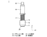
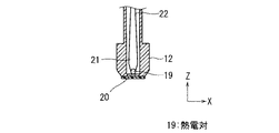
次に、図4と図5を用いて、スプリング方式の温度検出用プローブ7について説明する。図4は、温度検出用プローブ7の概略図であり、図5は、プランジャ部12の一部の概略断面図である。ここでは、プローブ7を構成するプランジャ部12の先端部分の内部に、測温部として熱電対19が設置された温度検出用プローブ7の例を示す。   Next, the spring-type temperature detection probe 7 will be described with reference to FIGS. 4 and 5. FIG. 4 is a schematic view of the temperature detection probe 7, and FIG. 5 is a schematic cross-sectional view of a part of the plunger portion 12. Here, an example of the temperature detection probe 7 in which a thermocouple 19 is installed as a temperature measuring part inside the tip portion of the plunger part 12 constituting the probe 7 is shown.

半導体装置5の評価の際、図2に示したように、スプリング方式の評価用プローブ10を半導体装置5の上面に設けた接続パッド18に接触させることは、評価用プローブ10と接続パッド18との電気的な導通が目的である。評価用、つまり、電気的な導通に用いるプローブ10とともに用いられる温度検出を目的としたスプリング方式の温度検出用プローブ7を採用することで、評価時の半導体装置5の温度を精度良く容易に得ることが可能となる。   When the semiconductor device 5 is evaluated, as shown in FIG. 2, when the spring-type evaluation probe 10 is brought into contact with the connection pad 18 provided on the upper surface of the semiconductor device 5, the evaluation probe 10, the connection pad 18, The purpose is electrical continuity. The temperature of the semiconductor device 5 at the time of evaluation can be obtained easily and accurately by employing the spring-type temperature detection probe 7 for the purpose of evaluation, that is, temperature detection used together with the probe 10 used for electrical conduction. It becomes possible.

図4に示すように、スプリング方式の温度検出用プローブ7は、評価用プローブ10の構成と同様に、プランジャ部12、バレル部14、バネ部材17、および端子部15を備えている。温度検出用プローブ7は、これらの構成に加えて測温部をさらに備えている。   As shown in FIG. 4, the spring-type temperature detection probe 7 includes a plunger portion 12, a barrel portion 14, a spring member 17, and a terminal portion 15, similarly to the configuration of the evaluation probe 10. In addition to these components, the temperature detection probe 7 further includes a temperature measuring unit.

プランジャ部12の先端部には半導体装置5と接触可能なコンタクト部11が設けられ、プランジャ部12の基端部には先端部分よりも細い円筒状の押し込み部13が設けられ、バネ部材17は押し込み部13に嵌められている。バレル部14は円筒状に形成され、押し込み部13の一部が挿入可能に構成されている。コンタクト部11にて半導体装置5と接触するプランジャ部12は可動部であり、バレル部14は、バネ部材17を介してプランジャ部12を半導体装置5側に押圧する。そして、押し込み部13の一部がバネ部材17を介して鉛直方向(+Z方向)に押し込まれることで、半導体装置5との接触を確実なものとする。   A contact portion 11 that can contact the semiconductor device 5 is provided at the distal end portion of the plunger portion 12, and a cylindrical pushing portion 13 that is thinner than the distal end portion is provided at the proximal end portion of the plunger portion 12. The push-in portion 13 is fitted. The barrel portion 14 is formed in a cylindrical shape, and a part of the push-in portion 13 can be inserted. The plunger portion 12 that comes into contact with the semiconductor device 5 at the contact portion 11 is a movable portion, and the barrel portion 14 presses the plunger portion 12 toward the semiconductor device 5 via the spring member 17. Then, a part of the pushing portion 13 is pushed in the vertical direction (+ Z direction) via the spring member 17, thereby ensuring contact with the semiconductor device 5.

プランジャ部12は、評価用であれば、導電性を有する、例えば銅、タングステンまたはレニウムタングステンなどの金属材料を用いて作製されるがこれらに限るものではなく、特に半導体装置5と接触するコンタクト部11は導電性向上および耐久性向上等の観点から、上記の金属材料に別の部材、例えば金、パラジウム、タンタルまたはプラチナ等を被覆した材料を用いて作製してもよい。ここでは温度検出用のため、導電性は必要なく、評価用のプローブを流用するのでなければ、熱伝導性を有する材料を、金属材料に限らず、利用できる。熱伝導性を向上させたフィラーを充填した樹脂などがこれにあたる。   For evaluation purposes, the plunger portion 12 is made of a conductive metal material such as copper, tungsten, or rhenium tungsten. However, the plunger portion 12 is not limited to this, and in particular, a contact portion that contacts the semiconductor device 5. 11 may be manufactured using a material obtained by coating the above metal material with another member, for example, gold, palladium, tantalum, platinum, or the like from the viewpoint of improving conductivity and durability. Here, for temperature detection, there is no need for conductivity, and a material having thermal conductivity can be used without being limited to a metal material unless the probe for evaluation is used. A resin filled with a filler with improved thermal conductivity corresponds to this.

バネ部材17は、プランジャ部12を容易に可動するために必要な部材であり、ここでは、外部に設ける構成とした。後述するように、プランジャ部12の内部に中空部が構成され、中空部に測温部から延長した配線が通されるため、プランジャ部12の内部空間の利用可能な体積が制限されるためである。   The spring member 17 is a member necessary for easily moving the plunger portion 12, and here, it is configured to be provided outside. As will be described later, since a hollow portion is formed inside the plunger portion 12 and a wire extending from the temperature measuring portion is passed through the hollow portion, the usable volume of the internal space of the plunger portion 12 is limited. is there.

しかしながら、大電流向けのプローブの場合などでは、プランジャ部12そのものの外径が大きく、内部空間にバネ部材17を設ける余裕がある場合もあり、バネ部材17の配置は外部に限るものではない。バレル部14は、スプリング方式の温度検出用プローブ7の基台となる部位であり、絶縁板16への固定の際に利用される。端子部15は、制御部4への出力のための結線部として用いられプランジャ部12の押し込み部13と電気的に接続され、両者は一体化された構成としてもよい。   However, in the case of a probe for a large current, the outer diameter of the plunger portion 12 itself is large, and there is a case where there is room for providing the spring member 17 in the internal space, and the arrangement of the spring member 17 is not limited to the outside. The barrel portion 14 is a portion that becomes a base of the spring-type temperature detection probe 7 and is used when being fixed to the insulating plate 16. The terminal unit 15 may be used as a connection unit for output to the control unit 4 and electrically connected to the pushing unit 13 of the plunger unit 12, and both may be integrated.

プランジャ部12を電気伝導性の材料で構成した場合、絶縁性材料の保護部20を、プランジャ部12のコンタクト部11に設ける必要がある。これは、スプリング方式の温度検出用プローブ7を従来の評価用プローブ10と共に絶縁板16の同等位置に配置した場合、半導体装置5に通電する半導体装置5の表面の接続パッド18と接触することになるが、このときスプリング方式の温度検出用プローブ7への、半導体装置5の評価のための通電を回避するためである。ただし、半導体装置5上の接続パッド18上などではなく絶縁膜上に、プランジャ部12のコンタクト部11を接触させる場合であれば、保護部20を設けなくてもよい。なお、保護部20は、熱伝導を阻害しない薄厚の素材で構成されることが望ましく、例えばテフロン(登録商標)であるが、これに限るものではない。   When the plunger portion 12 is made of an electrically conductive material, it is necessary to provide the insulating material protection portion 20 on the contact portion 11 of the plunger portion 12. This is because, when the spring-type temperature detection probe 7 is arranged at the same position of the insulating plate 16 together with the conventional evaluation probe 10, it contacts with the connection pads 18 on the surface of the semiconductor device 5 through which the semiconductor device 5 is energized. However, this is to avoid energization of the spring-type temperature detection probe 7 for evaluation of the semiconductor device 5 at this time. However, if the contact portion 11 of the plunger portion 12 is brought into contact with the insulating film instead of on the connection pad 18 on the semiconductor device 5, the protection portion 20 may not be provided. The protection unit 20 is preferably made of a thin material that does not hinder heat conduction, and is, for example, Teflon (registered trademark), but is not limited thereto.

次に、温度検出用プローブ7が備える測温部について説明する。図5に示すように、プランジャ部12の先端部分は円筒状に形成され、その外径は、評価用であれば、印加する電流に応じて一般的には5mm程度から10mm程度となる。測温部は熱電対19で構成され、温度検出用プローブ7では、熱電対19はプランジャ部12の内部に配置される。そのため、プランジャ部12の内部に少なくとも内径3mm程度の中空部21を有することから、プランジャ部12の外径は6mm以上となる。プランジャ部12を金属で作製する場合、中空部21は切削加工にて刳り抜いて作製される。   Next, the temperature measuring unit provided in the temperature detection probe 7 will be described. As shown in FIG. 5, the distal end portion of the plunger portion 12 is formed in a cylindrical shape, and its outer diameter is generally about 5 mm to 10 mm depending on the applied current for evaluation. The temperature measuring part is composed of a thermocouple 19, and in the temperature detection probe 7, the thermocouple 19 is arranged inside the plunger part 12. Therefore, since the inside of the plunger part 12 has the hollow part 21 with an inner diameter of at least about 3 mm, the outer diameter of the plunger part 12 is 6 mm or more. When the plunger portion 12 is made of metal, the hollow portion 21 is cut and produced by cutting.

熱電対19は、プランジャ部12の先端部の内部に配置されている。熱電対19は、2種類の異なる金属を接続して、両方の接点間にその温度差によって生じる起電力にて温度を検出するものであり、選択される金属材料としては、銅−コンスタンタン、またはクロメル−アルメル等があるがこれらに限らない。熱電対19の外径は、微小な箇所の温度検出用として、1mm程度での作製が可能である。熱電対19の配線22の一端側は、端子部15の上端から延び、制御部4に接続される。この例では、熱電対19をプランジャ部12の内部に外部から隔離して配置することから、熱電対19の外部環境からの保護を確実に行える。さらに、保護部20は、プランジャ部12を介して熱電対19の一部を覆っており、熱電対19を保護している。   The thermocouple 19 is disposed inside the distal end portion of the plunger portion 12. The thermocouple 19 connects two different metals and detects the temperature by an electromotive force generated by the temperature difference between the two contacts. As a selected metal material, copper-constantan, or Examples include, but are not limited to, chromel-alumel. The thermocouple 19 can be manufactured with an outer diameter of about 1 mm for temperature detection of a minute portion. One end side of the wiring 22 of the thermocouple 19 extends from the upper end of the terminal portion 15 and is connected to the control unit 4. In this example, since the thermocouple 19 is disposed inside the plunger portion 12 so as to be isolated from the outside, the thermocouple 19 can be reliably protected from the external environment. Further, the protection unit 20 covers a part of the thermocouple 19 via the plunger unit 12 to protect the thermocouple 19.

次に、温度検出用プローブ7の変形例について説明する。図6は、実施の形態の変形例1に係る温度検出用プローブ7のプランジャ部12の一部の概略断面図である。熱電対19をプランジャ部12の先端部の外部に配置した以外は、図5と同様であるため、重複する説明は省略する。図6に示すように、中空部21は、プランジャ部12の先端部を貫通した状態で設けられ、熱電対19の先端部はプランジャ部12の先端から突出した状態で配置されている。熱電対19が、直接、半導体装置5と接触することを回避するため、熱電対19は保護部20にて被覆されている。保護部20は、例えば熱伝導性を向上させたフィラーを充填した樹脂で構成されるが、これに限るものではない。本変形例1により、半導体装置5と測温部を一層近接して配置することができ、半導体装置5の温度の検出精度の向上を図ることが可能となる。   Next, a modification of the temperature detection probe 7 will be described. FIG. 6 is a schematic cross-sectional view of a part of the plunger portion 12 of the temperature detection probe 7 according to the first modification of the embodiment. Since it is the same as that of FIG. 5 except having arrange | positioned the thermocouple 19 outside the front-end | tip part of the plunger part 12, the overlapping description is abbreviate | omitted. As shown in FIG. 6, the hollow portion 21 is provided in a state of penetrating the distal end portion of the plunger portion 12, and the distal end portion of the thermocouple 19 is arranged in a state of protruding from the distal end of the plunger portion 12. In order to prevent the thermocouple 19 from coming into direct contact with the semiconductor device 5, the thermocouple 19 is covered with a protection unit 20. Although the protection part 20 is comprised with resin filled with the filler which improved thermal conductivity, for example, it is not restricted to this. According to the first modification, the semiconductor device 5 and the temperature measuring unit can be arranged closer to each other, and the temperature detection accuracy of the semiconductor device 5 can be improved.

図7は、実施の形態の変形例2に係る温度検出用プローブ7のプランジャ部12の一部の概略断面図であり、図8は、測温部設置治具31の概略斜視図である。図7に示すように、測温部は表面実装型のサーミスタ30で構成され、サーミスタ30が設置された測温部設置治具31を、プランジャ部12の先端部に嵌合することで配置した構成である。他の構成は上記の例と同様であり、説明を省略する。   FIG. 7 is a schematic cross-sectional view of a part of the plunger portion 12 of the temperature detection probe 7 according to Modification 2 of the embodiment, and FIG. 8 is a schematic perspective view of the temperature measuring portion installation jig 31. As shown in FIG. 7, the temperature measuring unit is composed of a surface mount type thermistor 30, and a temperature measuring unit installation jig 31 on which the thermistor 30 is installed is arranged by being fitted to the tip of the plunger unit 12. It is a configuration. Other configurations are the same as in the above example, and the description is omitted.

サーミスタ30は、測温抵抗体の一種であり、酸化物の電気抵抗変化を利用して温度を検出するものであって、その形態は、リード線を具備したものなど種々存在する。ここでは、小型化の観点から表面実装型の素子を選択したが、これに限るものではない。表面実装型であれば、その外形は、長辺で1mm程度となる。サーミスタ30が設置される測温部設置治具31は、電気伝導性を有する金属材料、例えば銅で構成され、板金加工で作製されるが、これに限るものではない。   The thermistor 30 is a kind of resistance temperature detector, and detects the temperature by using a change in electric resistance of an oxide, and there are various forms such as those having a lead wire. Here, a surface-mount type element is selected from the viewpoint of miniaturization, but the present invention is not limited to this. In the case of the surface mount type, the outer shape is about 1 mm on the long side. The temperature measuring unit installation jig 31 on which the thermistor 30 is installed is made of a metal material having electrical conductivity, such as copper, and is manufactured by sheet metal processing, but is not limited thereto.

測温部設置治具31は、略筒状の嵌合部32、および側面視にて略L字状の本体部33を備えている。本体部33の底部は、測温部設置部33aであり、測温部設置部33aの上面にサーミスタ30が設置されている。すなわち、測温部設置部33aは、サーミスタ30と半導体装置5との間に介在することになり、サーミスタ30を保護する機能を有する。さらに、測温部設置部33aは熱伝導性を有する板材料で構成されるため、半導体装置5の熱をサーミスタ30に効率よく伝達する機能を有する。   The temperature measuring portion installation jig 31 includes a substantially cylindrical fitting portion 32 and a substantially L-shaped main body portion 33 in a side view. The bottom part of the main body part 33 is a temperature measurement part installation part 33a, and the thermistor 30 is installed on the upper surface of the temperature measurement part installation part 33a. That is, the temperature measuring unit installation unit 33 a is interposed between the thermistor 30 and the semiconductor device 5 and has a function of protecting the thermistor 30. Furthermore, since the temperature measuring unit installation unit 33a is made of a plate material having thermal conductivity, it has a function of efficiently transferring the heat of the semiconductor device 5 to the thermistor 30.

図7に示すように、表面実装型のサーミスタ30の上下両端部に電極34,35がそれぞれ設けられている。電極35は、測温部設置部33aに半田付け等で、電気的かつ機械的に接続されている。電極34には配線22が接続されている。配線22の一端側は、端子部15の上端から延びている。電極35は、測温部設置治具31を介してプランジャ部12に接続され、さらには端子部15に接続されている。   As shown in FIG. 7, electrodes 34 and 35 are provided on both upper and lower ends of the surface mount type thermistor 30, respectively. The electrode 35 is electrically and mechanically connected to the temperature measuring portion installation portion 33a by soldering or the like. A wiring 22 is connected to the electrode 34. One end side of the wiring 22 extends from the upper end of the terminal portion 15. The electrode 35 is connected to the plunger portion 12 via the temperature measuring portion installation jig 31 and further connected to the terminal portion 15.

中空部21は2段階で形成されている。すなわち、中空部21におけるプランジャ部12の先端部分に対応する部分は貫通状に形成されるとともに、それ以外の部分よりも内径が大きくなるように形成されている。プランジャ部12の先端部分は、嵌合部32と嵌合され、電気的かつ機械的に測温部設置治具31と接続される。測温部設置治具31は、電気伝導性の材料で構成されるため、絶縁性材料で構成される絶縁部33bが、測温部設置部33aと半導体装置5との接触箇所(測温部設置部33aの下面)にさらに配置されている。ここで、測温部設置部33aが測温部であるサーミスタ30を保護するための保護部に相当する。   The hollow portion 21 is formed in two stages. That is, a portion of the hollow portion 21 corresponding to the distal end portion of the plunger portion 12 is formed in a penetrating shape and has an inner diameter larger than that of the other portions. The distal end portion of the plunger portion 12 is fitted with the fitting portion 32 and is electrically and mechanically connected to the temperature measuring portion installation jig 31. Since the temperature measuring portion installation jig 31 is made of an electrically conductive material, the insulating portion 33b made of an insulating material is a contact point between the temperature measuring portion setting portion 33a and the semiconductor device 5 (temperature measuring portion). It is further arranged on the lower surface of the installation portion 33a. Here, the temperature measurement unit installation unit 33a corresponds to a protection unit for protecting the thermistor 30 as the temperature measurement unit.

これにより、半導体装置5と測温部を一層近接して配置することができ、半導体装置5の温度の検出精度の向上を図ることが可能となる。また、測温部としてのサーミスタ30の故障時に交換が容易となる。   As a result, the semiconductor device 5 and the temperature measuring unit can be arranged closer to each other, and the temperature detection accuracy of the semiconductor device 5 can be improved. Moreover, replacement | exchange becomes easy at the time of failure of the thermistor 30 as a temperature measuring part.

なお、測温部としてサーミスタ30を用いた例を示したが、サーミスタ30に限るものではなく、白金抵抗体を用いてもよい。白金抵抗体とは、金属の電気抵抗が温度にほぼ比例して変化することを利用して温度を検出するものである。   In addition, although the example which used the thermistor 30 as a temperature measuring part was shown, it is not restricted to the thermistor 30, You may use a platinum resistor. The platinum resistor is a device that detects the temperature by utilizing the fact that the electric resistance of the metal changes almost in proportion to the temperature.

次に、測温部をプランジャ部12の内部に設けた、さらに別の変形例を図9に示す。図9は、実施の形態の変形例3に係る温度検出用プローブ7のプランジャ部12の一部の概略断面図である。図9に示すように、同軸型の2軸のコンタクトプローブを応用するものであり、2つの軸間に測温部を構成する表面実装型のサーミスタ30を配置した構成である。   Next, still another modified example in which the temperature measuring part is provided inside the plunger part 12 is shown in FIG. FIG. 9 is a schematic cross-sectional view of a part of the plunger portion 12 of the temperature detection probe 7 according to Modification 3 of the embodiment. As shown in FIG. 9, a coaxial biaxial contact probe is applied, and a surface mount type thermistor 30 constituting a temperature measuring unit is arranged between the two axes.

プランジャ部12は、第2電極軸37と、第2電極軸37の内部に配置される第1電極軸36とで構成されている。同軸型の2軸のコンタクトプローブにおいて、第1電極軸36および第2電極軸37は互いに絶縁され、それぞれ別個に出力される。第1電極軸36および第2電極軸37は、サーミスタ30の出力電極に接続されることで、サーミスタ30の出力を、各電極軸36,37の延長部である結線部から、それぞれ得ることが可能となる。また、サーミスタ30および各電極軸36,37と、半導体装置5との絶縁性を確保するために、プランジャ部12における半導体装置5と接触する箇所に絶縁性材料で作製された保護部20が配置されている。   The plunger portion 12 includes a second electrode shaft 37 and a first electrode shaft 36 disposed inside the second electrode shaft 37. In the coaxial biaxial contact probe, the first electrode shaft 36 and the second electrode shaft 37 are insulated from each other and output separately. The first electrode shaft 36 and the second electrode shaft 37 are connected to the output electrode of the thermistor 30 so that the output of the thermistor 30 can be obtained from the connection portion that is an extension of the electrode shafts 36 and 37, respectively. It becomes possible. In addition, in order to ensure insulation between the thermistor 30 and each of the electrode shafts 36 and 37 and the semiconductor device 5, a protective portion 20 made of an insulating material is disposed at a location where the plunger portion 12 contacts the semiconductor device 5. Has been.

なお、測温部としてサーミスタ30を用いた例を示したが、サーミスタ30に限るものではなく、白金抵抗体を用いてもよい。   In addition, although the example which used the thermistor 30 as a temperature measuring part was shown, it is not restricted to the thermistor 30, You may use a platinum resistor.

これにより、配線部分を介することなく測温部を設置できるため、設置および故障時における測温部の交換が容易となる。   Thereby, since a temperature measurement part can be installed without going through a wiring part, replacement | exchange of a temperature measurement part at the time of installation and a failure becomes easy.

なお、温度検出用プローブ7は、半導体装置5の電気的特性の評価時の温度を検出することを目的としたがこれに限るものではなく、例えば治具の温度またはプロセス途上の装置の温度などを接触して簡易に検出することにも利用可能である。   The temperature detection probe 7 is intended to detect the temperature at the time of evaluating the electrical characteristics of the semiconductor device 5, but is not limited to this. For example, the temperature of a jig or the temperature of a device in the process, etc. It can also be used for simple detection by touching.

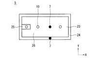
次に、絶縁板16に配置されるスプリング方式の温度検出用プローブ7の配置例について説明する。図10は、温度検出用プローブ7の配置構成の一例を示す概略図であり、より具体的には、評価時における1つの半導体装置5、評価用プローブ10、および温度検出用プローブ7を示した平面図である。なお、図面を簡単にするために絶縁板16は図示を省略し、温度検出用プローブ7の接触位置を黒丸、評価用プローブ10の接触位置を白丸で示すものとする。   Next, an arrangement example of the spring-type temperature detection probe 7 arranged on the insulating plate 16 will be described. FIG. 10 is a schematic diagram showing an example of the arrangement configuration of the temperature detection probe 7, and more specifically, shows one semiconductor device 5, the evaluation probe 10, and the temperature detection probe 7 at the time of evaluation. It is a top view. In order to simplify the drawing, the insulating plate 16 is not shown, and the contact position of the temperature detection probe 7 is indicated by a black circle, and the contact position of the evaluation probe 10 is indicated by a white circle.

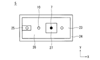
半導体装置5は、特に電力変換装置などに使用される高耐圧半導体装置であり、例えば、IGBT、MOSFET、またはダイオード等である。これらの高耐圧を示す半導体装置5は、電流を制御する活性領域23と、分離耐圧を持たせる終端領域24とを備えている。活性領域23は半導体装置5の中央部に設けられ、終端領域24は半導体装置5の周縁部に設けられている。半導体装置5は、以降IGBTを例として説明するが、その活性領域23には、外部との接続に用いられる接続パッドとして、ゲート電極25およびエミッタ電極26が設けられている。温度検出用プローブ7は、半導体装置5のエミッタ電極26の中央部に接触することで、当該箇所の温度検出を行う。すなわち、半導体装置5のエミッタ電極26中央部温度が、半導体装置5における活性領域23の表面温度の代表値として取り扱われる。   The semiconductor device 5 is a high voltage semiconductor device used particularly for a power conversion device, and is, for example, an IGBT, a MOSFET, or a diode. These semiconductor devices 5 exhibiting a high breakdown voltage include an active region 23 for controlling current and a termination region 24 for providing an isolation breakdown voltage. The active region 23 is provided in the central portion of the semiconductor device 5, and the termination region 24 is provided in the peripheral portion of the semiconductor device 5. The semiconductor device 5 will be described below using an IGBT as an example. In the active region 23, a gate electrode 25 and an emitter electrode 26 are provided as connection pads used for connection to the outside. The temperature detection probe 7 detects the temperature of the location by contacting the central portion of the emitter electrode 26 of the semiconductor device 5. That is, the temperature at the center of the emitter electrode 26 of the semiconductor device 5 is handled as a representative value of the surface temperature of the active region 23 in the semiconductor device 5.

ここで、例えば被測定物を囲むようにヒーターが配置され、ヒーターの内部に配置された温度検出用プローブが当該包囲形状内の中央部に位置する場合が考えられるが、これはヒーターによる加熱効果が最も及び難い領域として中央部を指定するものであり、本実施の形態とは構成と効果を異にする。   Here, for example, a heater may be disposed so as to surround the object to be measured, and a temperature detection probe disposed inside the heater may be located in the center of the surrounding shape. However, the central portion is designated as the most difficult region, and the configuration and effects are different from those of the present embodiment.

次に、温度検出用プローブ7の配置構成の他の例について説明する。図11、図12および図13は、温度検出用プローブ7の配置構成の他の例を示す概略図である。   Next, another example of the arrangement configuration of the temperature detection probe 7 will be described. 11, 12, and 13 are schematic diagrams illustrating other examples of the arrangement configuration of the temperature detection probes 7.

温度検出用プローブ7の配置は図10に限らず、図11に示すように、半導体装置5の終端領域24に温度検出用プローブ7が配置され、終端領域24の温度検出を行ってもよい。評価時における半導体装置5の破壊現象に伴う温度変化を検出する際、特に部分放電は半導体装置5の活性領域23だけでなく、終端領域24においても発生することが知られているためである。   The arrangement of the temperature detection probe 7 is not limited to FIG. 10, and as shown in FIG. 11, the temperature detection probe 7 may be arranged in the termination region 24 of the semiconductor device 5 to detect the temperature of the termination region 24. This is because, when detecting a temperature change accompanying the breakdown phenomenon of the semiconductor device 5 at the time of evaluation, it is known that a partial discharge particularly occurs not only in the active region 23 but also in the termination region 24 of the semiconductor device 5.

また、図12に示すように、中央領域である活性領域23と終端領域24に温度検出用プローブ7をそれぞれ配置し、活性領域23と終端領域24の温度を検出してもよい。複数個所の半導体装置5の表面温度を検出することで、半導体装置5の温度の均一性の評価が可能となり、破壊現象および部分放電の検出精度の向上を図ることが可能となる。   In addition, as shown in FIG. 12, the temperature detection probes 7 may be arranged in the active region 23 and the termination region 24, which are the central regions, and the temperatures of the active region 23 and the termination region 24 may be detected. By detecting the surface temperature of the semiconductor device 5 at a plurality of locations, it becomes possible to evaluate the uniformity of the temperature of the semiconductor device 5 and improve the detection accuracy of the breakdown phenomenon and partial discharge.

また、図13に示すように、エミッタ電極26上に配置された絶縁層27上に温度検出用プローブ7を接触させる構成でもよい。絶縁層27上に接触させるのであれば、保護部20は不要となる。絶縁層27の配置は、例えば終端領域24上の絶縁層の配置工程で作製可能であり、特に工程を追加する必要はない。   Further, as shown in FIG. 13, the temperature detection probe 7 may be brought into contact with an insulating layer 27 disposed on the emitter electrode 26. If it is made to contact on the insulating layer 27, the protection part 20 becomes unnecessary. The insulating layer 27 can be arranged, for example, in the step of arranging the insulating layer on the termination region 24, and there is no need to add any particular process.

次に、実施の形態に係る半導体装置の評価装置1の動作手順について説明する。複数の評価用プローブ10を有する場合、半導体装置5の電気的特性の評価前に、評価用プローブ10のコンタクト部11の平行度が揃えられる。温度検出用プローブ7は、先に半導体装置5の表面への接触が可能となるように、温度検出用プローブ7の先端部が、半導体装置5の電気的特性の評価前、正確に言えば半導体装置5にプローブを接触させる前の状態で、評価用プローブ10の先端部よりも下方に位置するように配置される。半導体装置5の設置面がチャックステージ3上に接触するように、半導体装置5はチャックステージ3上に載置される。半導体装置5は、例えば複数の半導体チップが形成された半導体ウエハまたは、半導体チップそのものが考えられるが、これに限るものではなく、真空吸着等によって固定される半導体装置であればよい。   Next, an operation procedure of the semiconductor device evaluation apparatus 1 according to the embodiment will be described. In the case of having a plurality of evaluation probes 10, the parallelism of the contact portions 11 of the evaluation probe 10 is made uniform before evaluating the electrical characteristics of the semiconductor device 5. Prior to the evaluation of the electrical characteristics of the semiconductor device 5, the temperature detection probe 7 is precisely the semiconductor so that the tip of the temperature detection probe 7 can be brought into contact with the surface of the semiconductor device 5 first. Before the probe is brought into contact with the device 5, the probe is arranged to be positioned below the tip of the evaluation probe 10. The semiconductor device 5 is placed on the chuck stage 3 so that the installation surface of the semiconductor device 5 is in contact with the chuck stage 3. The semiconductor device 5 may be, for example, a semiconductor wafer on which a plurality of semiconductor chips are formed, or the semiconductor chip itself, but is not limited thereto, and may be any semiconductor device that is fixed by vacuum suction or the like.

半導体装置5のチャックステージ3上への固定後、まず、制御部4は、温度検出用プローブ7を半導体装置5の表面と接触させ、半導体装置5の表面温度を検出し、所望の評価温度かどうかの確認を行う。所望の評価温度に至っていれば、制御部4は、評価用プローブ10を接続パッド18に接触させる。その後、制御部4は、所望の電気的特性に関する評価を実施するが、同時に、半導体装置5の表面温度の検出を継続する。これは、評価時の半導体装置5の正確な温度を検出するためであり、通電時の発熱による温度上昇、およびその後の冷却まで把握するためである。ここで、制御部4は、評価用プローブ10を介して半導体装置5の電気的特性を評価する評価部に相当する。   After fixing the semiconductor device 5 on the chuck stage 3, first, the control unit 4 brings the temperature detection probe 7 into contact with the surface of the semiconductor device 5, detects the surface temperature of the semiconductor device 5, and sets the desired evaluation temperature. Check if. If the desired evaluation temperature has been reached, the control unit 4 brings the evaluation probe 10 into contact with the connection pad 18. Thereafter, the control unit 4 performs the evaluation on the desired electrical characteristics, but at the same time, continues to detect the surface temperature of the semiconductor device 5. This is to detect the accurate temperature of the semiconductor device 5 at the time of evaluation, and to grasp the temperature rise due to heat generation during energization and subsequent cooling. Here, the control unit 4 corresponds to an evaluation unit that evaluates the electrical characteristics of the semiconductor device 5 via the evaluation probe 10.

なお、制御部4は、検出した温度が予め設定した値を越えたとき、つまり、異常な発熱、破壊現象、または部分放電等が発生したと判断したときは電気的特性の評価途中であっても、半導体装置5の電気的特性の評価を中止し、その評価を実施していた半導体装置5の位置を記憶する。これは、部分放電の発生した半導体装置5を、その後の工程から除去するためである。   When the detected temperature exceeds a preset value, that is, when it is determined that an abnormal heat generation, breakdown phenomenon, partial discharge or the like has occurred, the control unit 4 is in the process of evaluating the electrical characteristics. In addition, the evaluation of the electrical characteristics of the semiconductor device 5 is stopped, and the position of the semiconductor device 5 that has been evaluated is stored. This is because the semiconductor device 5 in which partial discharge has occurred is removed from the subsequent steps.

次に、実施の形態に係る温度検出用プローブ7、半導体装置の評価装置1および半導体装置の評価方法の効果について説明する。   Next, effects of the temperature detection probe 7, the semiconductor device evaluation apparatus 1, and the semiconductor device evaluation method according to the embodiment will be described.

実施の形態に係る温度検出用プローブ7では、バレル部14によってバネ部材17を介してプランジャ部12を半導体装置5側に押し込むことでプランジャ部12と半導体装置5との接触を確実なものとし、測温部で半導体装置5の温度を検出する。したがって、半導体装置5の電気的特性を評価する際に、半導体装置5の温度を精度よく検出することができる。   In the temperature detection probe 7 according to the embodiment, the plunger portion 12 is pushed into the semiconductor device 5 side by the barrel portion 14 via the spring member 17 to ensure the contact between the plunger portion 12 and the semiconductor device 5. The temperature measuring unit detects the temperature of the semiconductor device 5. Therefore, the temperature of the semiconductor device 5 can be accurately detected when evaluating the electrical characteristics of the semiconductor device 5.

また、温度検出用プローブ7は、バネ部材17を介してプランジャ部12を半導体装置5側に押圧する構成のため、カンチレバー方式の場合よりも半導体装置5から温度検出用プローブ7が接続される絶縁板16までの距離を離すことができ、気中放電を抑制できる。   Further, since the temperature detection probe 7 is configured to press the plunger portion 12 toward the semiconductor device 5 through the spring member 17, the insulation to which the temperature detection probe 7 is connected from the semiconductor device 5 is more than in the case of the cantilever type. The distance to the plate 16 can be increased, and air discharge can be suppressed.

測温部は、プランジャ部12の先端部の内部に配置されるため、測温部の外部環境からの保護を向上させることができる。   Since the temperature measuring unit is disposed inside the distal end portion of the plunger unit 12, the protection of the temperature measuring unit from the external environment can be improved.

プランジャ部12における半導体装置5と接触する箇所に保護部20が配置されるため、測温部を保護することができる。これにより、測温部の長寿命化を図ることが可能となる。   Since the protection part 20 is arrange | positioned in the location which contacts the semiconductor device 5 in the plunger part 12, a temperature measurement part can be protected. This makes it possible to extend the life of the temperature measuring unit.

保護部20は、測温部の少なくとも一部を覆う、熱伝導性を有する絶縁材料で構成されるため、半導体装置5の温度の検出精度を低下させることなく、容易に測温部を保護することができる。   Since the protection unit 20 is made of an insulating material having thermal conductivity that covers at least a part of the temperature measurement unit, the temperature measurement unit can be easily protected without reducing the temperature detection accuracy of the semiconductor device 5. be able to.

測温部は熱電対19で構成されるため、温度検出用プローブ7の小型化を容易に図ることができるとともに、プランジャ部12の内部への設置も容易に行うことができる。これにより、温度検出用プローブ7の歩留りの向上を図ることが可能となる。   Since the temperature measuring unit is composed of the thermocouple 19, the temperature detecting probe 7 can be easily reduced in size and can be easily installed inside the plunger unit 12. Thereby, the yield of the temperature detection probe 7 can be improved.

実施の形態の変形例1では、図6に示すように、測温部は、プランジャ部12の先端部の外部に配置されるため、半導体装置5と測温部をさらに近接することができ、半導体装置5の温度の検出精度が向上する。   In the first modification of the embodiment, as shown in FIG. 6, the temperature measuring unit is disposed outside the distal end portion of the plunger unit 12, so that the semiconductor device 5 and the temperature measuring unit can be brought closer to each other, The temperature detection accuracy of the semiconductor device 5 is improved.

実施の形態の変形例2では、図7に示すように、保護部である測温部設置部33aは、測温部と半導体装置5との間に介在させる、熱伝導性を有する板材料で構成される。したがって、半導体装置5の温度の検出精度を低下させることなく、容易に測温部を保護することができる。   In the second modification of the embodiment, as shown in FIG. 7, the temperature measuring unit installation unit 33 a that is a protection unit is a plate material having thermal conductivity that is interposed between the temperature measuring unit and the semiconductor device 5. Composed. Therefore, the temperature measuring unit can be easily protected without reducing the temperature detection accuracy of the semiconductor device 5.

実施の形態の変形例3では、図9に示すように、測温部は、プランジャ部12を構成する第1電極軸36と第2電極軸37との間に配置され、プランジャ部12における半導体装置5と接触する箇所に保護部20が配置されるため、測温部の設置と交換が容易となる。   In the third modification of the embodiment, as shown in FIG. 9, the temperature measuring unit is disposed between the first electrode shaft 36 and the second electrode shaft 37 constituting the plunger unit 12, and the semiconductor in the plunger unit 12. Since the protection part 20 is arrange | positioned in the location which contacts the apparatus 5, installation and replacement | exchange of a temperature measurement part become easy.

図7と図9に示すように、実施の形態の変形例2,3では、測温部は白金抵抗体またはサーミスタ30で構成される場合は、表面実装型の抵抗体を利用することで温度検出用プローブ7の小型化を容易に図ることができる。   As shown in FIGS. 7 and 9, in the second and third modifications of the embodiment, when the temperature measuring unit is composed of a platinum resistor or the thermistor 30, the temperature is measured by using a surface-mounted resistor. The size of the detection probe 7 can be easily reduced.

実施の形態に係る半導体装置の評価装置1は、温度検出用プローブ7と、半導体装置5を固定するためのチャックステージ3と、スプリング方式の評価用プローブ10と、評価用プローブ10を介して半導体装置5の電気的特性を評価する制御部4とを備える。したがって、半導体装置5の電気的特性を評価する際に、半導体装置5の温度を精度よく検出することができる。   The semiconductor device evaluation apparatus 1 according to the embodiment includes a temperature detection probe 7, a chuck stage 3 for fixing the semiconductor device 5, a spring-type evaluation probe 10, and a semiconductor via the evaluation probe 10. And a control unit 4 for evaluating the electrical characteristics of the device 5. Therefore, the temperature of the semiconductor device 5 can be accurately detected when evaluating the electrical characteristics of the semiconductor device 5.

また、温度検出用プローブ7は、バネ部材17を介してプランジャ部12を半導体装置5側に押圧する構成のため、カンチレバー方式の場合よりも半導体装置5から温度検出用プローブ7が接続される絶縁板16までの距離を離すことができ、気中放電を抑制できる。   Further, since the temperature detection probe 7 is configured to press the plunger portion 12 toward the semiconductor device 5 through the spring member 17, the insulation to which the temperature detection probe 7 is connected from the semiconductor device 5 is more than in the case of the cantilever type. The distance to the plate 16 can be increased, and air discharge can be suppressed.

半導体装置5の電気的特性の評価中に半導体装置5に生じた温度上昇から、簡易に部分放電の発生を検出することが可能であり、部分放電の発生を検出後、評価を即時に中止することで評価用プローブ10、温度検出用プローブ7および接続パッド等の破損を抑制できる。また、評価時に部分放電の発生した半導体装置5を特定することができ、その後の工程からその半導体装置5を排除することができる。これにより、評価後の部分放電発生の確認が不要となり、工程の短縮が可能となる。   It is possible to easily detect the occurrence of partial discharge from the temperature rise generated in the semiconductor device 5 during the evaluation of the electrical characteristics of the semiconductor device 5, and the evaluation is immediately stopped after the occurrence of partial discharge is detected. Thus, damage to the evaluation probe 10, the temperature detection probe 7, the connection pad, and the like can be suppressed. In addition, the semiconductor device 5 in which partial discharge has occurred during the evaluation can be specified, and the semiconductor device 5 can be excluded from the subsequent processes. This eliminates the need for confirmation of the occurrence of partial discharge after the evaluation, and shortens the process.

温度検出用プローブ7の先端部は、半導体装置5の電気的特性の評価前の状態で、評価用プローブ10の先端部よりも下方に位置するため、温度検出用プローブ7のみ前もって半導体装置5に接触させることができる。半導体装置5の表面温度の確認後に電気的特性の評価を行うことで、複数のプローブ接触による半導体装置5の温度が変化することを抑制できる。   Since the tip of the temperature detection probe 7 is positioned below the tip of the evaluation probe 10 in a state before the electrical characteristics of the semiconductor device 5 are evaluated, only the temperature detection probe 7 is connected to the semiconductor device 5 in advance. Can be contacted. By evaluating the electrical characteristics after confirming the surface temperature of the semiconductor device 5, it is possible to suppress a change in the temperature of the semiconductor device 5 due to a plurality of probe contacts.

図10に示すように、温度検出用プローブ7は、半導体装置5における活性領域23であるエミッタ電極26の中央部と接触可能に配置されるため、半導体装置5の活性領域23の温度を検出することができる。当該温度が電気的特性の評価時における半導体装置5の温度であると仮定され、半導体装置5の温度の代表値として取り扱われることで、温度検出用プローブ7の配置数を減らすことができ、低コスト化を図ることが可能となる。   As shown in FIG. 10, the temperature detection probe 7 is disposed so as to be able to come into contact with the central portion of the emitter electrode 26 that is the active region 23 in the semiconductor device 5, and therefore detects the temperature of the active region 23 of the semiconductor device 5. be able to. It is assumed that the temperature is the temperature of the semiconductor device 5 at the time of evaluating the electrical characteristics, and is handled as a representative value of the temperature of the semiconductor device 5. Cost can be reduced.

図11に示すように、温度検出用プローブ7が、半導体装置5の周縁部である終端領域24と接触可能に配置されるため、半導体装置5の終端領域24にて多発する放電などの破壊現象を検出することができる。   As shown in FIG. 11, since the temperature detection probe 7 is disposed so as to be in contact with the termination region 24 that is the peripheral portion of the semiconductor device 5, a breakdown phenomenon such as a discharge that frequently occurs in the termination region 24 of the semiconductor device 5. Can be detected.

図12に示すように、温度検出用プローブ7が、半導体装置5の活性領域23および終端領域24と接触可能に配置されるため、半導体装置5の活性領域23および終端領域24の温度を検出することで、半導体装置5の表面の温度を偏りなく検出することができる。また、半導体装置5における部分的な破壊時の温度異常も検出することができる。   As shown in FIG. 12, since the temperature detection probe 7 is disposed so as to be in contact with the active region 23 and the termination region 24 of the semiconductor device 5, the temperature of the active region 23 and the termination region 24 of the semiconductor device 5 is detected. Thus, the temperature of the surface of the semiconductor device 5 can be detected without deviation. Further, a temperature abnormality at the time of partial destruction in the semiconductor device 5 can also be detected.

なお、本実施の形態では、評価用プローブ10および温度検出用プローブ7を同一の絶縁板16に配置する構成としたがこれに限るものではなく、互いに異なる絶縁板に配置する構成でもよい。この場合、各プローブ7,10を、半導体装置5に対して個別に接触または非接触させることが可能となり、半導体装置5に対する押圧量を個別に調整できるため、半導体装置5に対して過度な負荷がかかることを抑制できる。これにより、半導体装置5の破損を抑制できる。   In the present embodiment, the evaluation probe 10 and the temperature detection probe 7 are arranged on the same insulating plate 16. However, the present invention is not limited to this, and the arrangement may be such that they are arranged on different insulating plates. In this case, the probes 7 and 10 can be individually brought into contact with or not brought into contact with the semiconductor device 5, and the pressing amount against the semiconductor device 5 can be individually adjusted. Can be suppressed. Thereby, damage to the semiconductor device 5 can be suppressed.

制御部4は、温度検出用プローブ7によって検出された半導体装置5の温度に基づいて、評価用プローブ10および評価部による半導体装置5の電気的特性の評価を制御するため、半導体装置5の温度の異常を検出後、評価終了前であっても評価を中止させることができる。これにより、評価用プローブ10、温度検出用プローブ7および接続パッド等の破損を抑制できる。   The control unit 4 controls the evaluation of the electrical characteristics of the semiconductor device 5 by the evaluation probe 10 and the evaluation unit based on the temperature of the semiconductor device 5 detected by the temperature detection probe 7. The evaluation can be stopped even after the abnormality is detected and before the evaluation is completed. Thereby, damage to the probe 10 for evaluation, the probe 7 for temperature detection, a connection pad, etc. can be suppressed.

実施の形態に係る半導体装置の評価方法は、評価用プローブ10および制御部4を用いて半導体装置5の電気的特性を評価する工程(a)と、温度検出用プローブ7を用いて、工程(a)による評価前および工程(a)による評価時における半導体装置5の表面の温度を検出する工程(b)とを備えるため、半導体装置5の表面の温度を簡易に精度よく検出することができる。また、上記と同様に気中放電を抑制できる。   The semiconductor device evaluation method according to the embodiment includes a step (a) of evaluating the electrical characteristics of the semiconductor device 5 using the evaluation probe 10 and the control unit 4, and a step ( and (b) detecting the temperature of the surface of the semiconductor device 5 before the evaluation according to a) and during the evaluation according to the step (a), the temperature of the surface of the semiconductor device 5 can be detected easily and accurately. . Moreover, air discharge can be suppressed similarly to the above.

半導体装置の評価方法は、工程(b)で検出された半導体装置5の表面の温度に基づいて、工程(a)による半導体装置5の電気的特性の評価を中止する工程(c)をさらに備えるため、半導体装置5の温度の異常を検出後、評価終了前であっても評価を中止させることができる。これにより、評価用プローブ10、温度検出用プローブ7および接続パッド等の破損を抑制できる。   The semiconductor device evaluation method further includes a step (c) of stopping the evaluation of the electrical characteristics of the semiconductor device 5 in the step (a) based on the surface temperature of the semiconductor device 5 detected in the step (b). Therefore, the evaluation can be stopped even after the evaluation is completed after the abnormality of the temperature of the semiconductor device 5 is detected. Thereby, damage to the probe 10 for evaluation, the probe 7 for temperature detection, a connection pad, etc. can be suppressed.

なお、本発明は、その発明の範囲内において、実施の形態を適宜、変形、省略することが可能である。   In the present invention, the embodiments can be appropriately modified and omitted within the scope of the invention.

1 評価装置、3 チャックステージ、4 制御部、5 半導体装置、7 温度検出用プローブ、10 評価用プローブ、12 プランジャ部、14 バレル部、16 絶縁板、17 バネ部材、19 熱電対、20 保護部、30 サーミスタ、33a 測温部設置部、36 第1電極軸、37 第2電極軸。   DESCRIPTION OF SYMBOLS 1 Evaluation apparatus, 3 Chuck stage, 4 Control part, 5 Semiconductor device, 7 Temperature detection probe, 10 Evaluation probe, 12 Plunger part, 14 Barrel part, 16 Insulating plate, 17 Spring member, 19 Thermocouple, 20 Protection part , 30 Thermistor, 33a Temperature measuring part installation part, 36 1st electrode axis, 37 2nd electrode axis.

Claims (18)

被測定物と接触可能なプランジャ部と、
前記プランジャ部の基端部に配置されるバネ部材と、
前記バネ部材を介して前記プランジャ部を前記被測定物側に押圧するバレル部と、
前記被測定物の温度を検出する測温部と、
を備える、コンタクトプローブ型温度検出器。
A plunger that can contact the object to be measured;
A spring member disposed at a proximal end portion of the plunger portion;
A barrel portion that presses the plunger portion toward the object to be measured via the spring member;
A temperature measuring unit for detecting the temperature of the object to be measured;
A contact probe type temperature detector.
前記測温部は、前記プランジャ部の先端部の内部に配置される、請求項1記載のコンタクトプローブ型温度検出器。   The contact probe type temperature detector according to claim 1, wherein the temperature measuring unit is disposed inside a distal end portion of the plunger unit. 前記測温部は、前記プランジャ部の先端部の外部に配置される、請求項1記載のコンタクトプローブ型温度検出器。   The contact probe type temperature detector according to claim 1, wherein the temperature measuring unit is disposed outside a tip portion of the plunger unit. 前記プランジャ部における前記被測定物と接触する箇所に保護部が配置される、請求項3記載のコンタクトプローブ型温度検出器。   The contact probe type temperature detector according to claim 3, wherein a protective part is arranged at a position where the plunger part comes into contact with the object to be measured. 前記保護部は、前記測温部の少なくとも一部を覆う、熱伝導性を有する絶縁材料で構成される、請求項4記載のコンタクトプローブ型温度検出器。   The contact probe type temperature detector according to claim 4, wherein the protection unit is made of an insulating material having thermal conductivity that covers at least a part of the temperature measurement unit. 前記保護部は、前記測温部と前記被測定物との間に介在させる、熱伝導性を有する板材料で構成される、請求項4記載のコンタクトプローブ型温度検出器。   The contact probe type temperature detector according to claim 4, wherein the protection unit is formed of a plate material having thermal conductivity interposed between the temperature measurement unit and the object to be measured. 前記測温部は、前記プランジャ部を構成する第1の電極軸と第2の電極軸との間に配置され、
前記プランジャ部における前記被測定物と接触する箇所に保護部が配置される、請求項2記載のコンタクトプローブ型温度検出器。
The temperature measuring unit is disposed between a first electrode shaft and a second electrode shaft constituting the plunger unit,
The contact probe type temperature detector according to claim 2, wherein a protective part is disposed at a position where the plunger part contacts the object to be measured.
前記測温部は熱電対で構成される、請求項1から請求項7のいずれか1つに記載のコンタクトプローブ型温度検出器。   The contact probe type temperature detector according to any one of claims 1 to 7, wherein the temperature measuring unit is configured by a thermocouple. 前記測温部は白金抵抗体またはサーミスタで構成される、請求項1から請求項7のいずれか1つに記載のコンタクトプローブ型温度検出器。   The contact probe type temperature detector according to any one of claims 1 to 7, wherein the temperature measuring unit is configured by a platinum resistor or a thermistor. 請求項1から請求項9のいずれか1つに記載のコンタクトプローブ型温度検出器と、
前記被測定物を固定するためのステージと、
スプリング方式の評価用プローブと、
前記評価用プローブを介して前記被測定物の電気的特性を評価する評価部と、
を備える、半導体装置の評価装置。
A contact probe type temperature detector according to any one of claims 1 to 9,
A stage for fixing the object to be measured;
A spring-type evaluation probe;
An evaluation unit for evaluating the electrical characteristics of the object to be measured via the evaluation probe;
An apparatus for evaluating a semiconductor device.
前記コンタクトプローブ型温度検出器の先端部は、前記被測定物の電気的特性の評価前の状態で、前記評価用プローブの先端部よりも下方に位置する、請求項10記載の半導体装置の評価装置。   The semiconductor device evaluation according to claim 10, wherein a front end portion of the contact probe type temperature detector is positioned below a front end portion of the evaluation probe in a state before evaluation of electrical characteristics of the object to be measured. apparatus. 前記コンタクトプローブ型温度検出器は、前記被測定物の中央部と接触可能に配置される、請求項10または請求項11記載の半導体装置の評価装置。   12. The evaluation apparatus for a semiconductor device according to claim 10, wherein the contact probe type temperature detector is arranged so as to be in contact with a central portion of the object to be measured. 前記コンタクトプローブ型温度検出器は、前記被測定物の周縁部と接触可能に配置される、請求項10または請求項11記載の半導体装置の評価装置。   12. The evaluation apparatus for a semiconductor device according to claim 10, wherein the contact probe type temperature detector is disposed so as to be in contact with a peripheral portion of the object to be measured. 前記コンタクトプローブ型温度検出器は、前記被測定物の中央部および周縁部と接触可能に配置される、請求項10または請求項11記載の半導体装置の評価装置。   The semiconductor device evaluation apparatus according to claim 10, wherein the contact probe type temperature detector is disposed so as to be able to contact a central portion and a peripheral portion of the object to be measured. 前記評価用プローブおよび前記コンタクトプローブ型温度検出器は、互いに異なる絶縁板に配置される、請求項10から請求項14のいずれか1つに記載の半導体装置の評価装置。   The semiconductor device evaluation apparatus according to claim 10, wherein the evaluation probe and the contact probe type temperature detector are arranged on different insulating plates. 前記コンタクトプローブ型温度検出器によって検出された前記被測定物の温度に基づいて、前記評価用プローブおよび前記評価部による前記被測定物の電気的特性の評価を制御する制御部をさらに備える、請求項10から請求項15のいずれか1つに記載の半導体装置の評価装置。   And a control unit that controls evaluation of electrical characteristics of the measurement object by the evaluation probe and the evaluation unit based on the temperature of the measurement object detected by the contact probe type temperature detector. The evaluation apparatus for a semiconductor device according to any one of claims 10 to 15. 請求項10から請求項16のいずれか1つに記載の半導体装置の評価装置を用いた半導体装置の評価方法であって、
(a)前記評価用プローブおよび前記評価部を用いて前記被測定物の電気的特性を評価する工程と、
(b)前記コンタクトプローブ型温度検出器を用いて、前記工程(a)による評価前および前記工程(a)による評価時における前記被測定物の表面の温度を検出する工程と、
を備える、半導体装置の評価方法。
A semiconductor device evaluation method using the semiconductor device evaluation device according to any one of claims 10 to 16,
(A) a step of evaluating electrical characteristics of the object to be measured using the evaluation probe and the evaluation unit;
(B) using the contact probe type temperature detector, detecting the temperature of the surface of the object to be measured before the evaluation by the step (a) and at the time of the evaluation by the step (a);
A method for evaluating a semiconductor device.
(c)前記工程(b)で検出された前記被測定物の表面の温度に基づいて、前記工程(a)による前記被測定物の電気的特性の評価を中止する工程をさらに備える、請求項17記載の半導体装置の評価方法。 (C) The method further comprises the step of stopping the evaluation of the electrical characteristics of the device under test (a) based on the temperature of the surface of the device under test detected in the step (b). 18. The method for evaluating a semiconductor device according to 17.
JP2015125432A 2015-06-23 2015-06-23 Contact probe type temperature detector, evaluation device of semiconductor device and evaluation method of semiconductor device Pending JP2017009449A (en)

Priority Applications (3)

Application Number Priority Date Filing Date Title
JP2015125432A JP2017009449A (en) 2015-06-23 2015-06-23 Contact probe type temperature detector, evaluation device of semiconductor device and evaluation method of semiconductor device
US15/064,054 US20160377486A1 (en) 2015-06-23 2016-03-08 Contact-probe type temperature detector, semiconductor device evaluation apparatus and semiconductor device evaluating method
CN201610466367.1A CN106291302A (en) 2015-06-23 2016-06-23 Contact probe type temperature detector, the evaluating apparatus of semiconductor device and the evaluation methodology of semiconductor device

Applications Claiming Priority (1)

Application Number Priority Date Filing Date Title
JP2015125432A JP2017009449A (en) 2015-06-23 2015-06-23 Contact probe type temperature detector, evaluation device of semiconductor device and evaluation method of semiconductor device

Publications (1)

Publication Number Publication Date
JP2017009449A true JP2017009449A (en) 2017-01-12

Family

ID=57602076

Family Applications (1)

Application Number Title Priority Date Filing Date
JP2015125432A Pending JP2017009449A (en) 2015-06-23 2015-06-23 Contact probe type temperature detector, evaluation device of semiconductor device and evaluation method of semiconductor device

Country Status (3)

Country Link
US (1) US20160377486A1 (en)
JP (1) JP2017009449A (en)
CN (1) CN106291302A (en)

Cited By (1)

* Cited by examiner, † Cited by third party
Publication number Priority date Publication date Assignee Title
JP2020106454A (en) * 2018-12-28 2020-07-09 東京エレクトロン株式会社 Temperature measuring member, inspection device, and temperature measurement method

Families Citing this family (6)

* Cited by examiner, † Cited by third party
Publication number Priority date Publication date Assignee Title
EP3682511A4 (en) * 2017-09-11 2021-05-12 Smiths Interconnect Americas, Inc. Spring probe connector for interfacing a printed circuit board with a backplane
CN108507705A (en) * 2018-07-04 2018-09-07 上海捷策创电子科技有限公司 A kind of chip temperature measuring equipment
TWI704354B (en) * 2019-03-21 2020-09-11 創意電子股份有限公司 Probe card, wafer inspection apparatus having the same, and chip probe test flow using the same
CN112067966B (en) * 2020-09-19 2022-07-05 哈尔滨理工大学 Simulation type IGBT failure mechanism analysis system
CN214335132U (en) 2021-01-13 2021-10-01 迪科特测试科技(苏州)有限公司 Detection system and detection device
CN113701909B (en) * 2021-08-24 2022-09-30 深圳市智佳能自动化有限公司 Thermocouple temperature measurement system for semiconductor seal measurement equipment

Family Cites Families (11)

* Cited by examiner, † Cited by third party
Publication number Priority date Publication date Assignee Title
US4241289A (en) * 1979-03-02 1980-12-23 General Electric Company Heat sensing apparatus for an electric range automatic surface unit control
US4444990A (en) * 1982-09-08 1984-04-24 Servo Corporation Of America Heat sensing device
JP2977189B2 (en) * 1996-01-26 1999-11-10 アスカ電子株式会社 Conductive contact pin
US5911897A (en) * 1997-01-13 1999-06-15 Micro Control Company Temperature control for high power burn-in for integrated circuits
JP3364677B2 (en) * 1998-07-14 2003-01-08 ジャパンシステムエンジニアリング株式会社 Rechargeable battery inspection device
US7123037B2 (en) * 2004-02-27 2006-10-17 Wells-Cti, Llc Integrated circuit temperature sensing device and method
US7728613B2 (en) * 2006-11-20 2010-06-01 Analog Devices, Inc. Device under test pogo pin type contact element
US20100301332A1 (en) * 2009-05-29 2010-12-02 Donald Dibra Detecting a Fault State of a Semiconductor Arrangement
CN201844890U (en) * 2010-09-17 2011-05-25 江苏绿叶锅炉有限公司 Temperature sensing probe
JP5673608B2 (en) * 2012-06-04 2015-02-18 三菱電機株式会社 Inspection apparatus and inspection method
JP6084469B2 (en) * 2013-01-28 2017-02-22 三菱電機株式会社 Semiconductor evaluation apparatus and semiconductor evaluation method

Cited By (2)

* Cited by examiner, † Cited by third party
Publication number Priority date Publication date Assignee Title
JP2020106454A (en) * 2018-12-28 2020-07-09 東京エレクトロン株式会社 Temperature measuring member, inspection device, and temperature measurement method
JP7153556B2 (en) 2018-12-28 2022-10-14 東京エレクトロン株式会社 Temperature measurement member, inspection device and temperature measurement method

Also Published As

Publication number Publication date
CN106291302A (en) 2017-01-04
US20160377486A1 (en) 2016-12-29

Similar Documents

Publication Publication Date Title
JP2017009449A (en) Contact probe type temperature detector, evaluation device of semiconductor device and evaluation method of semiconductor device
JP5737536B2 (en) Prober
JP6351763B2 (en) Semiconductor device evaluation jig, semiconductor device evaluation device, and semiconductor device evaluation method
EP3367108A1 (en) Probe card and contact inspection device
CN107037346B (en) Evaluation device and evaluation method for semiconductor device
TWI502204B (en) Electric connecting apparatus
CN108254667B (en) Evaluation device and evaluation method
CN102308432A (en) Cell temperature measurement device, cell temperature measurement method and cell production method
US10495668B2 (en) Evaluation apparatus for semiconductor device and evaluation method for semiconductor device
JP5562320B2 (en) Semiconductor test apparatus and semiconductor test method
JP4999775B2 (en) Prober
JP4602181B2 (en) Socket for semiconductor inspection
JP6418070B2 (en) Measuring device, measuring method of semiconductor device
JP6365953B1 (en) Prober
JP2007024702A5 (en)
JP2014103228A (en) Method for evaluating semiconductor device
JP5987637B2 (en) Evaluation device
JP2016065755A (en) Method for manufacturing temperature measurement sensor and temperature measurement sensor
EP2980840B1 (en) Probe device
JP5748709B2 (en) Probe card
JP2007129090A (en) Wafer test system, prober, wafer test method and probe card
JP2012178599A (en) Prober and temperature control method of the same
JP2009097860A (en) Electrical connection method and electrical connecting device
KR20160146043A (en) Proving chamber
JP2023005270A (en) Electronic component testing device