JP6813574B2 - インジウムまたはインジウム合金の堆積方法および物品 - Google Patents
インジウムまたはインジウム合金の堆積方法および物品 Download PDFInfo
- Publication number
- JP6813574B2 JP6813574B2 JP2018517570A JP2018517570A JP6813574B2 JP 6813574 B2 JP6813574 B2 JP 6813574B2 JP 2018517570 A JP2018517570 A JP 2018517570A JP 2018517570 A JP2018517570 A JP 2018517570A JP 6813574 B2 JP6813574 B2 JP 6813574B2
- Authority
- JP
- Japan
- Prior art keywords
- indium
- alloy
- metal
- layer
- nickel
- Prior art date
- Legal status (The legal status is an assumption and is not a legal conclusion. Google has not performed a legal analysis and makes no representation as to the accuracy of the status listed.)
- Active
Links
- APFVFJFRJDLVQX-UHFFFAOYSA-N indium atom Chemical compound [In] APFVFJFRJDLVQX-UHFFFAOYSA-N 0.000 title claims description 261
- 229910000846 In alloy Inorganic materials 0.000 title claims description 191
- 238000000151 deposition Methods 0.000 title claims description 93
- 229910052738 indium Inorganic materials 0.000 claims description 260
- 238000000034 method Methods 0.000 claims description 82
- 239000012071 phase Substances 0.000 claims description 78
- 229910052751 metal Inorganic materials 0.000 claims description 76
- 239000002184 metal Substances 0.000 claims description 76
- 230000008021 deposition Effects 0.000 claims description 74
- 239000002131 composite material Substances 0.000 claims description 59
- 229910001092 metal group alloy Inorganic materials 0.000 claims description 55
- 239000000758 substrate Substances 0.000 claims description 44
- PXHVJJICTQNCMI-UHFFFAOYSA-N Nickel Chemical compound [Ni] PXHVJJICTQNCMI-UHFFFAOYSA-N 0.000 claims description 42
- 229910052759 nickel Inorganic materials 0.000 claims description 19
- 229910000521 B alloy Inorganic materials 0.000 claims description 14
- 229910045601 alloy Inorganic materials 0.000 claims description 13
- 239000000956 alloy Substances 0.000 claims description 13
- 229910001096 P alloy Inorganic materials 0.000 claims description 12
- 150000002739 metals Chemical class 0.000 claims description 8
- 229910000990 Ni alloy Inorganic materials 0.000 claims description 6
- KJTLSVCANCCWHF-UHFFFAOYSA-N Ruthenium Chemical compound [Ru] KJTLSVCANCCWHF-UHFFFAOYSA-N 0.000 claims description 5
- 229910052707 ruthenium Inorganic materials 0.000 claims description 5
- ZOXJGFHDIHLPTG-UHFFFAOYSA-N Boron Chemical compound [B] ZOXJGFHDIHLPTG-UHFFFAOYSA-N 0.000 claims description 4
- OAICVXFJPJFONN-UHFFFAOYSA-N Phosphorus Chemical compound [P] OAICVXFJPJFONN-UHFFFAOYSA-N 0.000 claims description 4
- 229910052796 boron Inorganic materials 0.000 claims description 4
- 229910052698 phosphorus Inorganic materials 0.000 claims description 4
- 239000011574 phosphorus Substances 0.000 claims description 4
- WFKWXMTUELFFGS-UHFFFAOYSA-N tungsten Chemical compound [W] WFKWXMTUELFFGS-UHFFFAOYSA-N 0.000 claims description 4
- 229910052721 tungsten Inorganic materials 0.000 claims description 4
- 239000010937 tungsten Substances 0.000 claims description 4
- 238000001947 vapour-phase growth Methods 0.000 claims description 4
- RTAQQCXQSZGOHL-UHFFFAOYSA-N Titanium Chemical compound [Ti] RTAQQCXQSZGOHL-UHFFFAOYSA-N 0.000 claims description 3
- 229910017052 cobalt Inorganic materials 0.000 claims description 3
- 239000010941 cobalt Substances 0.000 claims description 3
- GUTLYIVDDKVIGB-UHFFFAOYSA-N cobalt atom Chemical compound [Co] GUTLYIVDDKVIGB-UHFFFAOYSA-N 0.000 claims description 3
- 229910052715 tantalum Inorganic materials 0.000 claims description 3
- GUVRBAGPIYLISA-UHFFFAOYSA-N tantalum atom Chemical compound [Ta] GUVRBAGPIYLISA-UHFFFAOYSA-N 0.000 claims description 3
- 239000010936 titanium Substances 0.000 claims description 3
- 229910052719 titanium Inorganic materials 0.000 claims description 3
- AFLIFFSIRLUWRH-UHFFFAOYSA-N [B].[P].[Mn].[Ni] Chemical compound [B].[P].[Mn].[Ni] AFLIFFSIRLUWRH-UHFFFAOYSA-N 0.000 claims description 2
- NSHBVFDIVYORDO-UHFFFAOYSA-N [Mn].[B].[Ni] Chemical compound [Mn].[B].[Ni] NSHBVFDIVYORDO-UHFFFAOYSA-N 0.000 claims description 2
- OZUHTGWWTWNDFY-UHFFFAOYSA-N [P].[B].[Ni].[Mo] Chemical compound [P].[B].[Ni].[Mo] OZUHTGWWTWNDFY-UHFFFAOYSA-N 0.000 claims description 2
- VRXREIYDGMTERC-UHFFFAOYSA-N [P].[Mn].[Ni] Chemical compound [P].[Mn].[Ni] VRXREIYDGMTERC-UHFFFAOYSA-N 0.000 claims description 2
- ACVSDIKGGNSZDR-UHFFFAOYSA-N [P].[W].[Ni] Chemical compound [P].[W].[Ni] ACVSDIKGGNSZDR-UHFFFAOYSA-N 0.000 claims description 2
- HMSUGMKVSFPDNC-UHFFFAOYSA-N [W].[B].[P].[Ni] Chemical compound [W].[B].[P].[Ni] HMSUGMKVSFPDNC-UHFFFAOYSA-N 0.000 claims description 2
- IJIMPXOIJZHGTP-UHFFFAOYSA-N boranylidynemolybdenum nickel Chemical compound [Ni].B#[Mo] IJIMPXOIJZHGTP-UHFFFAOYSA-N 0.000 claims description 2
- QDWJUBJKEHXSMT-UHFFFAOYSA-N boranylidynenickel Chemical compound [Ni]#B QDWJUBJKEHXSMT-UHFFFAOYSA-N 0.000 claims description 2
- IGLTYURFTAWDMX-UHFFFAOYSA-N boranylidynetungsten nickel Chemical compound [Ni].B#[W] IGLTYURFTAWDMX-UHFFFAOYSA-N 0.000 claims description 2
- 150000004767 nitrides Chemical class 0.000 claims description 2
- OFNHPGDEEMZPFG-UHFFFAOYSA-N phosphanylidynenickel Chemical compound [P].[Ni] OFNHPGDEEMZPFG-UHFFFAOYSA-N 0.000 claims description 2
- 229910021332 silicide Inorganic materials 0.000 claims description 2
- 239000000126 substance Substances 0.000 claims description 2
- CKQGJVKHBSPKST-UHFFFAOYSA-N [Ni].P#[Mo] Chemical compound [Ni].P#[Mo] CKQGJVKHBSPKST-UHFFFAOYSA-N 0.000 claims 1
- 238000000926 separation method Methods 0.000 claims 1
- 238000007747 plating Methods 0.000 description 77
- -1 halide ions Chemical class 0.000 description 23
- 229910001449 indium ion Inorganic materials 0.000 description 21
- RYGMFSIKBFXOCR-UHFFFAOYSA-N Copper Chemical compound [Cu] RYGMFSIKBFXOCR-UHFFFAOYSA-N 0.000 description 15
- 229910052802 copper Inorganic materials 0.000 description 15
- 239000010949 copper Substances 0.000 description 15
- 239000002253 acid Substances 0.000 description 14
- 230000015572 biosynthetic process Effects 0.000 description 13
- KRKNYBCHXYNGOX-UHFFFAOYSA-N citric acid Chemical compound OC(=O)CC(O)(C(O)=O)CC(O)=O KRKNYBCHXYNGOX-UHFFFAOYSA-N 0.000 description 12
- 230000008569 process Effects 0.000 description 12
- 239000002738 chelating agent Substances 0.000 description 11
- 150000002471 indium Chemical class 0.000 description 11
- 229910021645 metal ion Inorganic materials 0.000 description 11
- 150000003839 salts Chemical class 0.000 description 11
- XLYOFNOQVPJJNP-UHFFFAOYSA-N water Substances O XLYOFNOQVPJJNP-UHFFFAOYSA-N 0.000 description 10
- 229910052739 hydrogen Inorganic materials 0.000 description 9
- 239000001257 hydrogen Substances 0.000 description 9
- OFOBLEOULBTSOW-UHFFFAOYSA-N Malonic acid Chemical class OC(=O)CC(O)=O OFOBLEOULBTSOW-UHFFFAOYSA-N 0.000 description 8
- QAOWNCQODCNURD-UHFFFAOYSA-N Sulfuric acid Chemical compound OS(O)(=O)=O QAOWNCQODCNURD-UHFFFAOYSA-N 0.000 description 8
- 238000004299 exfoliation Methods 0.000 description 7
- UFHFLCQGNIYNRP-UHFFFAOYSA-N Hydrogen Chemical compound [H][H] UFHFLCQGNIYNRP-UHFFFAOYSA-N 0.000 description 6
- 230000000052 comparative effect Effects 0.000 description 6
- 239000004065 semiconductor Substances 0.000 description 6
- 239000004094 surface-active agent Substances 0.000 description 6
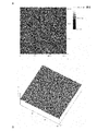
- 238000012876 topography Methods 0.000 description 6
- 230000002378 acidificating effect Effects 0.000 description 5
- 150000007513 acids Chemical class 0.000 description 5
- 230000004888 barrier function Effects 0.000 description 5
- 239000007788 liquid Substances 0.000 description 5
- 239000000203 mixture Substances 0.000 description 5
- 229910052709 silver Inorganic materials 0.000 description 5
- 239000004332 silver Substances 0.000 description 5
- 229910000679 solder Inorganic materials 0.000 description 5
- BJEPYKJPYRNKOW-REOHCLBHSA-N (S)-malic acid Chemical compound OC(=O)[C@@H](O)CC(O)=O BJEPYKJPYRNKOW-REOHCLBHSA-N 0.000 description 4
- LSNNMFCWUKXFEE-UHFFFAOYSA-M Bisulfite Chemical compound OS([O-])=O LSNNMFCWUKXFEE-UHFFFAOYSA-M 0.000 description 4
- FEWJPZIEWOKRBE-JCYAYHJZSA-N Dextrotartaric acid Chemical compound OC(=O)[C@H](O)[C@@H](O)C(O)=O FEWJPZIEWOKRBE-JCYAYHJZSA-N 0.000 description 4
- GYHNNYVSQQEPJS-UHFFFAOYSA-N Gallium Chemical compound [Ga] GYHNNYVSQQEPJS-UHFFFAOYSA-N 0.000 description 4
- DHMQDGOQFOQNFH-UHFFFAOYSA-N Glycine Chemical compound NCC(O)=O DHMQDGOQFOQNFH-UHFFFAOYSA-N 0.000 description 4
- AEMRFAOFKBGASW-UHFFFAOYSA-N Glycolic acid Chemical compound OCC(O)=O AEMRFAOFKBGASW-UHFFFAOYSA-N 0.000 description 4
- AFVFQIVMOAPDHO-UHFFFAOYSA-N Methanesulfonic acid Chemical compound CS(O)(=O)=O AFVFQIVMOAPDHO-UHFFFAOYSA-N 0.000 description 4
- KDLHZDBZIXYQEI-UHFFFAOYSA-N Palladium Chemical compound [Pd] KDLHZDBZIXYQEI-UHFFFAOYSA-N 0.000 description 4
- BQCADISMDOOEFD-UHFFFAOYSA-N Silver Chemical compound [Ag] BQCADISMDOOEFD-UHFFFAOYSA-N 0.000 description 4
- ATJFFYVFTNAWJD-UHFFFAOYSA-N Tin Chemical compound [Sn] ATJFFYVFTNAWJD-UHFFFAOYSA-N 0.000 description 4
- FEBFYWHXKVOHDI-UHFFFAOYSA-N [Co].[P][W] Chemical compound [Co].[P][W] FEBFYWHXKVOHDI-UHFFFAOYSA-N 0.000 description 4
- 229910002065 alloy metal Inorganic materials 0.000 description 4
- BJEPYKJPYRNKOW-UHFFFAOYSA-N alpha-hydroxysuccinic acid Natural products OC(=O)C(O)CC(O)=O BJEPYKJPYRNKOW-UHFFFAOYSA-N 0.000 description 4
- 239000007864 aqueous solution Substances 0.000 description 4
- 229910052797 bismuth Inorganic materials 0.000 description 4
- JCXGWMGPZLAOME-UHFFFAOYSA-N bismuth atom Chemical compound [Bi] JCXGWMGPZLAOME-UHFFFAOYSA-N 0.000 description 4
- 239000000969 carrier Substances 0.000 description 4
- 235000015165 citric acid Nutrition 0.000 description 4
- 150000002170 ethers Chemical class 0.000 description 4
- 229910052733 gallium Inorganic materials 0.000 description 4
- HHLFWLYXYJOTON-UHFFFAOYSA-N glyoxylic acid Chemical compound OC(=O)C=O HHLFWLYXYJOTON-UHFFFAOYSA-N 0.000 description 4
- 239000001630 malic acid Substances 0.000 description 4
- 235000011090 malic acid Nutrition 0.000 description 4
- 238000004519 manufacturing process Methods 0.000 description 4
- YGSDEFSMJLZEOE-UHFFFAOYSA-N salicylic acid Chemical compound OC(=O)C1=CC=CC=C1O YGSDEFSMJLZEOE-UHFFFAOYSA-N 0.000 description 4
- 230000003746 surface roughness Effects 0.000 description 4
- 239000011135 tin Substances 0.000 description 4
- 229910052718 tin Inorganic materials 0.000 description 4
- KCXVZYZYPLLWCC-UHFFFAOYSA-N EDTA Chemical compound OC(=O)CN(CC(O)=O)CCN(CC(O)=O)CC(O)=O KCXVZYZYPLLWCC-UHFFFAOYSA-N 0.000 description 3
- VEXZGXHMUGYJMC-UHFFFAOYSA-N Hydrochloric acid Chemical compound Cl VEXZGXHMUGYJMC-UHFFFAOYSA-N 0.000 description 3
- 229910021607 Silver chloride Inorganic materials 0.000 description 3
- FEWJPZIEWOKRBE-UHFFFAOYSA-N Tartaric acid Natural products [H+].[H+].[O-]C(=O)C(O)C(O)C([O-])=O FEWJPZIEWOKRBE-UHFFFAOYSA-N 0.000 description 3
- HCHKCACWOHOZIP-UHFFFAOYSA-N Zinc Chemical compound [Zn] HCHKCACWOHOZIP-UHFFFAOYSA-N 0.000 description 3
- 239000000654 additive Substances 0.000 description 3
- 229910052782 aluminium Inorganic materials 0.000 description 3
- XAGFODPZIPBFFR-UHFFFAOYSA-N aluminium Chemical compound [Al] XAGFODPZIPBFFR-UHFFFAOYSA-N 0.000 description 3
- 150000001735 carboxylic acids Chemical class 0.000 description 3
- 238000005137 deposition process Methods 0.000 description 3
- 238000005530 etching Methods 0.000 description 3
- PCHJSUWPFVWCPO-UHFFFAOYSA-N gold Chemical compound [Au] PCHJSUWPFVWCPO-UHFFFAOYSA-N 0.000 description 3
- 229910052737 gold Inorganic materials 0.000 description 3
- 239000010931 gold Substances 0.000 description 3
- 150000004679 hydroxides Chemical class 0.000 description 3
- 239000000463 material Substances 0.000 description 3
- 230000008018 melting Effects 0.000 description 3
- 238000002844 melting Methods 0.000 description 3
- 238000013508 migration Methods 0.000 description 3
- 230000005012 migration Effects 0.000 description 3
- LNOPIUAQISRISI-UHFFFAOYSA-N n'-hydroxy-2-propan-2-ylsulfonylethanimidamide Chemical class CC(C)S(=O)(=O)CC(N)=NO LNOPIUAQISRISI-UHFFFAOYSA-N 0.000 description 3
- 238000004886 process control Methods 0.000 description 3
- HKZLPVFGJNLROG-UHFFFAOYSA-M silver monochloride Chemical compound [Cl-].[Ag+] HKZLPVFGJNLROG-UHFFFAOYSA-M 0.000 description 3
- 239000002904 solvent Substances 0.000 description 3
- 150000003460 sulfonic acids Chemical class 0.000 description 3
- 239000011975 tartaric acid Substances 0.000 description 3
- 235000002906 tartaric acid Nutrition 0.000 description 3
- 229910052725 zinc Inorganic materials 0.000 description 3
- 239000011701 zinc Substances 0.000 description 3
- RBNPOMFGQQGHHO-UHFFFAOYSA-N -2,3-Dihydroxypropanoic acid Natural products OCC(O)C(O)=O RBNPOMFGQQGHHO-UHFFFAOYSA-N 0.000 description 2
- LBLYYCQCTBFVLH-UHFFFAOYSA-N 2-Methylbenzenesulfonic acid Chemical compound CC1=CC=CC=C1S(O)(=O)=O LBLYYCQCTBFVLH-UHFFFAOYSA-N 0.000 description 2
- NEAQRZUHTPSBBM-UHFFFAOYSA-N 2-hydroxy-3,3-dimethyl-7-nitro-4h-isoquinolin-1-one Chemical class C1=C([N+]([O-])=O)C=C2C(=O)N(O)C(C)(C)CC2=C1 NEAQRZUHTPSBBM-UHFFFAOYSA-N 0.000 description 2
- SJZRECIVHVDYJC-UHFFFAOYSA-N 4-hydroxybutyric acid Chemical compound OCCCC(O)=O SJZRECIVHVDYJC-UHFFFAOYSA-N 0.000 description 2
- WDJHALXBUFZDSR-UHFFFAOYSA-N Acetoacetic acid Natural products CC(=O)CC(O)=O WDJHALXBUFZDSR-UHFFFAOYSA-N 0.000 description 2
- QGZKDVFQNNGYKY-UHFFFAOYSA-N Ammonia Chemical compound N QGZKDVFQNNGYKY-UHFFFAOYSA-N 0.000 description 2
- 239000004475 Arginine Substances 0.000 description 2
- DCXYFEDJOCDNAF-UHFFFAOYSA-N Asparagine Natural products OC(=O)C(N)CC(N)=O DCXYFEDJOCDNAF-UHFFFAOYSA-N 0.000 description 2
- XFXPMWWXUTWYJX-UHFFFAOYSA-N Cyanide Chemical compound N#[C-] XFXPMWWXUTWYJX-UHFFFAOYSA-N 0.000 description 2
- RBNPOMFGQQGHHO-UWTATZPHSA-N D-glyceric acid Chemical compound OC[C@@H](O)C(O)=O RBNPOMFGQQGHHO-UWTATZPHSA-N 0.000 description 2
- LYCAIKOWRPUZTN-UHFFFAOYSA-N Ethylene glycol Chemical compound OCCO LYCAIKOWRPUZTN-UHFFFAOYSA-N 0.000 description 2
- WQZGKKKJIJFFOK-GASJEMHNSA-N Glucose Natural products OC[C@H]1OC(O)[C@H](O)[C@@H](O)[C@@H]1O WQZGKKKJIJFFOK-GASJEMHNSA-N 0.000 description 2
- WHUUTDBJXJRKMK-UHFFFAOYSA-N Glutamic acid Natural products OC(=O)C(N)CCC(O)=O WHUUTDBJXJRKMK-UHFFFAOYSA-N 0.000 description 2
- 239000004471 Glycine Substances 0.000 description 2
- MHAJPDPJQMAIIY-UHFFFAOYSA-N Hydrogen peroxide Chemical compound OO MHAJPDPJQMAIIY-UHFFFAOYSA-N 0.000 description 2
- ODKSFYDXXFIFQN-BYPYZUCNSA-P L-argininium(2+) Chemical compound NC(=[NH2+])NCCC[C@H]([NH3+])C(O)=O ODKSFYDXXFIFQN-BYPYZUCNSA-P 0.000 description 2
- DCXYFEDJOCDNAF-REOHCLBHSA-N L-asparagine Chemical compound OC(=O)[C@@H](N)CC(N)=O DCXYFEDJOCDNAF-REOHCLBHSA-N 0.000 description 2
- CKLJMWTZIZZHCS-REOHCLBHSA-N L-aspartic acid Chemical compound OC(=O)[C@@H](N)CC(O)=O CKLJMWTZIZZHCS-REOHCLBHSA-N 0.000 description 2
- WHUUTDBJXJRKMK-VKHMYHEASA-N L-glutamic acid Chemical compound OC(=O)[C@@H](N)CCC(O)=O WHUUTDBJXJRKMK-VKHMYHEASA-N 0.000 description 2
- ZDXPYRJPNDTMRX-VKHMYHEASA-N L-glutamine Chemical compound OC(=O)[C@@H](N)CCC(N)=O ZDXPYRJPNDTMRX-VKHMYHEASA-N 0.000 description 2
- AGPKZVBTJJNPAG-WHFBIAKZSA-N L-isoleucine Chemical class CC[C@H](C)[C@H](N)C(O)=O AGPKZVBTJJNPAG-WHFBIAKZSA-N 0.000 description 2
- ROHFNLRQFUQHCH-YFKPBYRVSA-N L-leucine Chemical compound CC(C)C[C@H](N)C(O)=O ROHFNLRQFUQHCH-YFKPBYRVSA-N 0.000 description 2
- KDXKERNSBIXSRK-YFKPBYRVSA-N L-lysine Chemical compound NCCCC[C@H](N)C(O)=O KDXKERNSBIXSRK-YFKPBYRVSA-N 0.000 description 2
- AYFVYJQAPQTCCC-GBXIJSLDSA-N L-threonine Chemical compound C[C@@H](O)[C@H](N)C(O)=O AYFVYJQAPQTCCC-GBXIJSLDSA-N 0.000 description 2
- KZSNJWFQEVHDMF-BYPYZUCNSA-N L-valine Chemical class CC(C)[C@H](N)C(O)=O KZSNJWFQEVHDMF-BYPYZUCNSA-N 0.000 description 2
- ROHFNLRQFUQHCH-UHFFFAOYSA-N Leucine Natural products CC(C)CC(N)C(O)=O ROHFNLRQFUQHCH-UHFFFAOYSA-N 0.000 description 2
- KDXKERNSBIXSRK-UHFFFAOYSA-N Lysine Natural products NCCCCC(N)C(O)=O KDXKERNSBIXSRK-UHFFFAOYSA-N 0.000 description 2
- 239000004472 Lysine Substances 0.000 description 2
- 239000002202 Polyethylene glycol Substances 0.000 description 2
- 229920002873 Polyethylenimine Polymers 0.000 description 2
- LCTONWCANYUPML-UHFFFAOYSA-M Pyruvate Chemical compound CC(=O)C([O-])=O LCTONWCANYUPML-UHFFFAOYSA-M 0.000 description 2
- XUIMIQQOPSSXEZ-UHFFFAOYSA-N Silicon Chemical compound [Si] XUIMIQQOPSSXEZ-UHFFFAOYSA-N 0.000 description 2
- FAPWRFPIFSIZLT-UHFFFAOYSA-M Sodium chloride Chemical compound [Na+].[Cl-] FAPWRFPIFSIZLT-UHFFFAOYSA-M 0.000 description 2
- KDYFGRWQOYBRFD-UHFFFAOYSA-N Succinic acid Natural products OC(=O)CCC(O)=O KDYFGRWQOYBRFD-UHFFFAOYSA-N 0.000 description 2
- AYFVYJQAPQTCCC-UHFFFAOYSA-N Threonine Natural products CC(O)C(N)C(O)=O AYFVYJQAPQTCCC-UHFFFAOYSA-N 0.000 description 2
- 239000004473 Threonine Substances 0.000 description 2
- KZSNJWFQEVHDMF-UHFFFAOYSA-N Valine Chemical class CC(C)C(N)C(O)=O KZSNJWFQEVHDMF-UHFFFAOYSA-N 0.000 description 2
- DGEZNRSVGBDHLK-UHFFFAOYSA-N [1,10]phenanthroline Chemical compound C1=CN=C2C3=NC=CC=C3C=CC2=C1 DGEZNRSVGBDHLK-UHFFFAOYSA-N 0.000 description 2
- 150000001335 aliphatic alkanes Chemical class 0.000 description 2
- 229940024606 amino acid Drugs 0.000 description 2
- 235000001014 amino acid Nutrition 0.000 description 2
- 150000001413 amino acids Chemical class 0.000 description 2
- 229960003121 arginine Drugs 0.000 description 2
- ODKSFYDXXFIFQN-UHFFFAOYSA-N arginine Natural products OC(=O)C(N)CCCNC(N)=N ODKSFYDXXFIFQN-UHFFFAOYSA-N 0.000 description 2
- 235000009697 arginine Nutrition 0.000 description 2
- 229960001230 asparagine Drugs 0.000 description 2
- 235000009582 asparagine Nutrition 0.000 description 2
- 229960005261 aspartic acid Drugs 0.000 description 2
- 235000003704 aspartic acid Nutrition 0.000 description 2
- SRSXLGNVWSONIS-UHFFFAOYSA-N benzenesulfonic acid Chemical compound OS(=O)(=O)C1=CC=CC=C1 SRSXLGNVWSONIS-UHFFFAOYSA-N 0.000 description 2
- 229940092714 benzenesulfonic acid Drugs 0.000 description 2
- OQFSQFPPLPISGP-UHFFFAOYSA-N beta-carboxyaspartic acid Natural products OC(=O)C(N)C(C(O)=O)C(O)=O OQFSQFPPLPISGP-UHFFFAOYSA-N 0.000 description 2
- 229920001400 block copolymer Polymers 0.000 description 2
- KDYFGRWQOYBRFD-NUQCWPJISA-N butanedioic acid Chemical compound O[14C](=O)CC[14C](O)=O KDYFGRWQOYBRFD-NUQCWPJISA-N 0.000 description 2
- 239000008367 deionised water Substances 0.000 description 2
- 229910021641 deionized water Inorganic materials 0.000 description 2
- WOWBFOBYOAGEEA-UHFFFAOYSA-N diafenthiuron Chemical compound CC(C)C1=C(NC(=S)NC(C)(C)C)C(C(C)C)=CC(OC=2C=CC=CC=2)=C1 WOWBFOBYOAGEEA-UHFFFAOYSA-N 0.000 description 2
- 238000001035 drying Methods 0.000 description 2
- 238000009713 electroplating Methods 0.000 description 2
- CCIVGXIOQKPBKL-UHFFFAOYSA-M ethanesulfonate Chemical compound CCS([O-])(=O)=O CCIVGXIOQKPBKL-UHFFFAOYSA-M 0.000 description 2
- 239000007789 gas Substances 0.000 description 2
- 239000008103 glucose Substances 0.000 description 2
- 235000013922 glutamic acid Nutrition 0.000 description 2
- 229960002989 glutamic acid Drugs 0.000 description 2
- 239000004220 glutamic acid Substances 0.000 description 2
- ZDXPYRJPNDTMRX-UHFFFAOYSA-N glutamine Natural products OC(=O)C(N)CCC(N)=O ZDXPYRJPNDTMRX-UHFFFAOYSA-N 0.000 description 2
- 229960002743 glutamine Drugs 0.000 description 2
- 229960002449 glycine Drugs 0.000 description 2
- 150000004820 halides Chemical class 0.000 description 2
- 239000012535 impurity Substances 0.000 description 2
- 150000002500 ions Chemical class 0.000 description 2
- 229960000310 isoleucine Drugs 0.000 description 2
- AGPKZVBTJJNPAG-UHFFFAOYSA-N isoleucine Natural products CCC(C)C(N)C(O)=O AGPKZVBTJJNPAG-UHFFFAOYSA-N 0.000 description 2
- 239000011133 lead Substances 0.000 description 2
- 229960003136 leucine Drugs 0.000 description 2
- 229960003646 lysine Drugs 0.000 description 2
- 238000005259 measurement Methods 0.000 description 2
- 239000002609 medium Substances 0.000 description 2
- 229940098779 methanesulfonic acid Drugs 0.000 description 2
- 229910052763 palladium Inorganic materials 0.000 description 2
- FJKROLUGYXJWQN-UHFFFAOYSA-N papa-hydroxy-benzoic acid Natural products OC(=O)C1=CC=C(O)C=C1 FJKROLUGYXJWQN-UHFFFAOYSA-N 0.000 description 2
- 229920002120 photoresistant polymer Polymers 0.000 description 2
- 230000000704 physical effect Effects 0.000 description 2
- 229920001223 polyethylene glycol Polymers 0.000 description 2
- 229920000642 polymer Polymers 0.000 description 2
- 239000002994 raw material Substances 0.000 description 2
- 229960004889 salicylic acid Drugs 0.000 description 2
- 238000004062 sedimentation Methods 0.000 description 2
- 239000000243 solution Substances 0.000 description 2
- 238000003756 stirring Methods 0.000 description 2
- CWERGRDVMFNCDR-UHFFFAOYSA-N thioglycolic acid Chemical compound OC(=O)CS CWERGRDVMFNCDR-UHFFFAOYSA-N 0.000 description 2
- 229960002898 threonine Drugs 0.000 description 2
- 229960004295 valine Drugs 0.000 description 2
- 239000004474 valine Chemical class 0.000 description 2
- REJSMTWFWDLMQN-UHFFFAOYSA-N 3-(3-sulfopropylsulfanyl)propane-1-sulfonic acid Chemical compound OS(=O)(=O)CCCSCCCS(O)(=O)=O REJSMTWFWDLMQN-UHFFFAOYSA-N 0.000 description 1
- BMYNFMYTOJXKLE-UHFFFAOYSA-N 3-azaniumyl-2-hydroxypropanoate Chemical compound NCC(O)C(O)=O BMYNFMYTOJXKLE-UHFFFAOYSA-N 0.000 description 1
- OBDVFOBWBHMJDG-UHFFFAOYSA-N 3-mercapto-1-propanesulfonic acid Chemical compound OS(=O)(=O)CCCS OBDVFOBWBHMJDG-UHFFFAOYSA-N 0.000 description 1
- LUENVHHLGFLMFJ-UHFFFAOYSA-N 4-[(4-sulfophenyl)disulfanyl]benzenesulfonic acid Chemical compound C1=CC(S(=O)(=O)O)=CC=C1SSC1=CC=C(S(O)(=O)=O)C=C1 LUENVHHLGFLMFJ-UHFFFAOYSA-N 0.000 description 1
- 229910001369 Brass Inorganic materials 0.000 description 1
- VEXZGXHMUGYJMC-UHFFFAOYSA-M Chloride anion Chemical compound [Cl-] VEXZGXHMUGYJMC-UHFFFAOYSA-M 0.000 description 1
- 229910000881 Cu alloy Inorganic materials 0.000 description 1
- BRLQWZUYTZBJKN-UHFFFAOYSA-N Epichlorohydrin Chemical compound ClCC1CO1 BRLQWZUYTZBJKN-UHFFFAOYSA-N 0.000 description 1
- 229910002651 NO3 Inorganic materials 0.000 description 1
- NHNBFGGVMKEFGY-UHFFFAOYSA-N Nitrate Chemical compound [O-][N+]([O-])=O NHNBFGGVMKEFGY-UHFFFAOYSA-N 0.000 description 1
- MUBZPKHOEPUJKR-UHFFFAOYSA-N Oxalic acid Chemical compound OC(=O)C(O)=O MUBZPKHOEPUJKR-UHFFFAOYSA-N 0.000 description 1
- 239000004698 Polyethylene Substances 0.000 description 1
- BUGBHKTXTAQXES-UHFFFAOYSA-N Selenium Chemical compound [Se] BUGBHKTXTAQXES-UHFFFAOYSA-N 0.000 description 1
- DBMJMQXJHONAFJ-UHFFFAOYSA-M Sodium laurylsulphate Chemical compound [Na+].CCCCCCCCCCCCOS([O-])(=O)=O DBMJMQXJHONAFJ-UHFFFAOYSA-M 0.000 description 1
- 239000004141 Sodium laurylsulphate Substances 0.000 description 1
- NINIDFKCEFEMDL-UHFFFAOYSA-N Sulfur Chemical compound [S] NINIDFKCEFEMDL-UHFFFAOYSA-N 0.000 description 1
- GSEJCLTVZPLZKY-UHFFFAOYSA-N Triethanolamine Chemical compound OCCN(CCO)CCO GSEJCLTVZPLZKY-UHFFFAOYSA-N 0.000 description 1
- 101710149792 Triosephosphate isomerase, chloroplastic Proteins 0.000 description 1
- 101710195516 Triosephosphate isomerase, glycosomal Proteins 0.000 description 1
- ZCJHFOLNXNSZJG-UHFFFAOYSA-N [Na].NS(O)(=O)=O Chemical compound [Na].NS(O)(=O)=O ZCJHFOLNXNSZJG-UHFFFAOYSA-N 0.000 description 1
- 239000003929 acidic solution Substances 0.000 description 1
- 230000004913 activation Effects 0.000 description 1
- 230000000996 additive effect Effects 0.000 description 1
- 239000003570 air Substances 0.000 description 1
- 150000001298 alcohols Chemical class 0.000 description 1
- 229920002214 alkoxylated polymer Polymers 0.000 description 1
- 150000001412 amines Chemical class 0.000 description 1
- 229910021529 ammonia Inorganic materials 0.000 description 1
- 239000002280 amphoteric surfactant Substances 0.000 description 1
- 239000003945 anionic surfactant Substances 0.000 description 1
- 239000012736 aqueous medium Substances 0.000 description 1
- 125000003118 aryl group Chemical group 0.000 description 1
- 230000009286 beneficial effect Effects 0.000 description 1
- 230000008901 benefit Effects 0.000 description 1
- 238000009835 boiling Methods 0.000 description 1
- KGBXLFKZBHKPEV-UHFFFAOYSA-N boric acid Chemical compound OB(O)O KGBXLFKZBHKPEV-UHFFFAOYSA-N 0.000 description 1
- 239000004327 boric acid Substances 0.000 description 1
- 239000010951 brass Substances 0.000 description 1
- 150000001649 bromium compounds Chemical class 0.000 description 1
- QDHFHIQKOVNCNC-UHFFFAOYSA-N butane-1-sulfonic acid Chemical compound CCCCS(O)(=O)=O QDHFHIQKOVNCNC-UHFFFAOYSA-N 0.000 description 1
- BVKZGUZCCUSVTD-UHFFFAOYSA-N carbonic acid Chemical class OC(O)=O BVKZGUZCCUSVTD-UHFFFAOYSA-N 0.000 description 1
- 150000004649 carbonic acid derivatives Chemical class 0.000 description 1
- 150000001732 carboxylic acid derivatives Chemical class 0.000 description 1
- 239000003093 cationic surfactant Substances 0.000 description 1
- 238000006243 chemical reaction Methods 0.000 description 1
- 238000004140 cleaning Methods 0.000 description 1
- 239000003086 colorant Substances 0.000 description 1
- 230000002860 competitive effect Effects 0.000 description 1
- 150000004696 coordination complex Chemical class 0.000 description 1
- 230000007797 corrosion Effects 0.000 description 1
- 238000005260 corrosion Methods 0.000 description 1
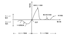
- 238000002484 cyclic voltammetry Methods 0.000 description 1
- 238000005238 degreasing Methods 0.000 description 1
- 230000032798 delamination Effects 0.000 description 1
- 230000001419 dependent effect Effects 0.000 description 1
- 238000010586 diagram Methods 0.000 description 1
- 125000000118 dimethyl group Chemical group [H]C([H])([H])* 0.000 description 1
- JZKFHQMONDVVNF-UHFFFAOYSA-N dodecyl sulfate;tris(2-hydroxyethyl)azanium Chemical compound OCCN(CCO)CCO.CCCCCCCCCCCCOS(O)(=O)=O JZKFHQMONDVVNF-UHFFFAOYSA-N 0.000 description 1
- 230000009977 dual effect Effects 0.000 description 1
- 230000000694 effects Effects 0.000 description 1
- 238000000840 electrochemical analysis Methods 0.000 description 1
- 230000005518 electrochemistry Effects 0.000 description 1
- 238000005868 electrolysis reaction Methods 0.000 description 1
- 239000003792 electrolyte Substances 0.000 description 1
- 239000011532 electronic conductor Substances 0.000 description 1
- 150000002148 esters Chemical class 0.000 description 1
- 230000005496 eutectics Effects 0.000 description 1
- 238000002474 experimental method Methods 0.000 description 1
- 238000009472 formulation Methods 0.000 description 1
- 231100000086 high toxicity Toxicity 0.000 description 1
- 150000002431 hydrogen Chemical class 0.000 description 1
- XLYOFNOQVPJJNP-UHFFFAOYSA-M hydroxide Chemical compound [OH-] XLYOFNOQVPJJNP-UHFFFAOYSA-M 0.000 description 1
- WGCNASOHLSPBMP-UHFFFAOYSA-N hydroxyacetaldehyde Natural products OCC=O WGCNASOHLSPBMP-UHFFFAOYSA-N 0.000 description 1
- 229910003437 indium oxide Inorganic materials 0.000 description 1
- 229910000337 indium(III) sulfate Inorganic materials 0.000 description 1
- PSCMQHVBLHHWTO-UHFFFAOYSA-K indium(iii) chloride Chemical class Cl[In](Cl)Cl PSCMQHVBLHHWTO-UHFFFAOYSA-K 0.000 description 1
- PJXISJQVUVHSOJ-UHFFFAOYSA-N indium(iii) oxide Chemical class [O-2].[O-2].[O-2].[In+3].[In+3] PJXISJQVUVHSOJ-UHFFFAOYSA-N 0.000 description 1
- XGCKLPDYTQRDTR-UHFFFAOYSA-H indium(iii) sulfate Chemical compound [In+3].[In+3].[O-]S([O-])(=O)=O.[O-]S([O-])(=O)=O.[O-]S([O-])(=O)=O XGCKLPDYTQRDTR-UHFFFAOYSA-H 0.000 description 1
- 239000011261 inert gas Substances 0.000 description 1
- 238000011835 investigation Methods 0.000 description 1
- 230000013011 mating Effects 0.000 description 1
- 229910052757 nitrogen Inorganic materials 0.000 description 1
- 239000002736 nonionic surfactant Substances 0.000 description 1
- 125000002347 octyl group Chemical group [H]C([*])([H])C([H])([H])C([H])([H])C([H])([H])C([H])([H])C([H])([H])C([H])([H])C([H])([H])[H] 0.000 description 1
- 239000007800 oxidant agent Substances 0.000 description 1
- 230000001590 oxidative effect Effects 0.000 description 1
- AMWVZPDSWLOFKA-UHFFFAOYSA-N phosphanylidynemolybdenum Chemical compound [Mo]#P AMWVZPDSWLOFKA-UHFFFAOYSA-N 0.000 description 1
- 239000006069 physical mixture Substances 0.000 description 1
- 238000005554 pickling Methods 0.000 description 1
- 229920001521 polyalkylene glycol ether Polymers 0.000 description 1
- 229920000573 polyethylene Polymers 0.000 description 1
- 230000003389 potentiating effect Effects 0.000 description 1
- 239000002244 precipitate Substances 0.000 description 1
- 238000012545 processing Methods 0.000 description 1
- 239000000047 product Substances 0.000 description 1
- 239000002516 radical scavenger Substances 0.000 description 1
- 239000013049 sediment Substances 0.000 description 1
- 229910052711 selenium Inorganic materials 0.000 description 1
- 239000011669 selenium Substances 0.000 description 1
- 230000035945 sensitivity Effects 0.000 description 1
- 229910052710 silicon Inorganic materials 0.000 description 1
- 239000010703 silicon Substances 0.000 description 1
- 239000011780 sodium chloride Substances 0.000 description 1
- 235000019333 sodium laurylsulphate Nutrition 0.000 description 1
- 229910052717 sulfur Inorganic materials 0.000 description 1
- 239000011593 sulfur Substances 0.000 description 1
- 229940095064 tartrate Drugs 0.000 description 1
- 125000000999 tert-butyl group Chemical group [H]C([H])([H])C(*)(C([H])([H])[H])C([H])([H])[H] 0.000 description 1
- 230000001988 toxicity Effects 0.000 description 1
- 231100000419 toxicity Toxicity 0.000 description 1
- 125000000391 vinyl group Chemical group [H]C([*])=C([H])[H] 0.000 description 1
- 229920002554 vinyl polymer Polymers 0.000 description 1
- 238000011179 visual inspection Methods 0.000 description 1
- 238000004832 voltammetry Methods 0.000 description 1
- 238000005406 washing Methods 0.000 description 1
Images


Classifications
-
- C—CHEMISTRY; METALLURGY
- C23—COATING METALLIC MATERIAL; COATING MATERIAL WITH METALLIC MATERIAL; CHEMICAL SURFACE TREATMENT; DIFFUSION TREATMENT OF METALLIC MATERIAL; COATING BY VACUUM EVAPORATION, BY SPUTTERING, BY ION IMPLANTATION OR BY CHEMICAL VAPOUR DEPOSITION, IN GENERAL; INHIBITING CORROSION OF METALLIC MATERIAL OR INCRUSTATION IN GENERAL
- C23C—COATING METALLIC MATERIAL; COATING MATERIAL WITH METALLIC MATERIAL; SURFACE TREATMENT OF METALLIC MATERIAL BY DIFFUSION INTO THE SURFACE, BY CHEMICAL CONVERSION OR SUBSTITUTION; COATING BY VACUUM EVAPORATION, BY SPUTTERING, BY ION IMPLANTATION OR BY CHEMICAL VAPOUR DEPOSITION, IN GENERAL
- C23C18/00—Chemical coating by decomposition of either liquid compounds or solutions of the coating forming compounds, without leaving reaction products of surface material in the coating; Contact plating
- C23C18/16—Chemical coating by decomposition of either liquid compounds or solutions of the coating forming compounds, without leaving reaction products of surface material in the coating; Contact plating by reduction or substitution, e.g. electroless plating
- C23C18/1601—Process or apparatus
- C23C18/1633—Process of electroless plating
- C23C18/1646—Characteristics of the product obtained
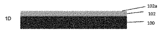
- C23C18/165—Multilayered product
- C23C18/1653—Two or more layers with at least one layer obtained by electroless plating and one layer obtained by electroplating
-
- C—CHEMISTRY; METALLURGY
- C25—ELECTROLYTIC OR ELECTROPHORETIC PROCESSES; APPARATUS THEREFOR
- C25D—PROCESSES FOR THE ELECTROLYTIC OR ELECTROPHORETIC PRODUCTION OF COATINGS; ELECTROFORMING; APPARATUS THEREFOR
- C25D5/00—Electroplating characterised by the process; Pretreatment or after-treatment of workpieces
- C25D5/10—Electroplating with more than one layer of the same or of different metals
- C25D5/12—Electroplating with more than one layer of the same or of different metals at least one layer being of nickel or chromium
-
- C—CHEMISTRY; METALLURGY
- C23—COATING METALLIC MATERIAL; COATING MATERIAL WITH METALLIC MATERIAL; CHEMICAL SURFACE TREATMENT; DIFFUSION TREATMENT OF METALLIC MATERIAL; COATING BY VACUUM EVAPORATION, BY SPUTTERING, BY ION IMPLANTATION OR BY CHEMICAL VAPOUR DEPOSITION, IN GENERAL; INHIBITING CORROSION OF METALLIC MATERIAL OR INCRUSTATION IN GENERAL
- C23C—COATING METALLIC MATERIAL; COATING MATERIAL WITH METALLIC MATERIAL; SURFACE TREATMENT OF METALLIC MATERIAL BY DIFFUSION INTO THE SURFACE, BY CHEMICAL CONVERSION OR SUBSTITUTION; COATING BY VACUUM EVAPORATION, BY SPUTTERING, BY ION IMPLANTATION OR BY CHEMICAL VAPOUR DEPOSITION, IN GENERAL
- C23C28/00—Coating for obtaining at least two superposed coatings either by methods not provided for in a single one of groups C23C2/00 - C23C26/00 or by combinations of methods provided for in subclasses C23C and C25C or C25D
- C23C28/02—Coating for obtaining at least two superposed coatings either by methods not provided for in a single one of groups C23C2/00 - C23C26/00 or by combinations of methods provided for in subclasses C23C and C25C or C25D only coatings only including layers of metallic material
- C23C28/021—Coating for obtaining at least two superposed coatings either by methods not provided for in a single one of groups C23C2/00 - C23C26/00 or by combinations of methods provided for in subclasses C23C and C25C or C25D only coatings only including layers of metallic material including at least one metal alloy layer
-
- C—CHEMISTRY; METALLURGY
- C25—ELECTROLYTIC OR ELECTROPHORETIC PROCESSES; APPARATUS THEREFOR
- C25D—PROCESSES FOR THE ELECTROLYTIC OR ELECTROPHORETIC PRODUCTION OF COATINGS; ELECTROFORMING; APPARATUS THEREFOR
- C25D5/00—Electroplating characterised by the process; Pretreatment or after-treatment of workpieces
- C25D5/10—Electroplating with more than one layer of the same or of different metals
-
- C—CHEMISTRY; METALLURGY
- C25—ELECTROLYTIC OR ELECTROPHORETIC PROCESSES; APPARATUS THEREFOR
- C25D—PROCESSES FOR THE ELECTROLYTIC OR ELECTROPHORETIC PRODUCTION OF COATINGS; ELECTROFORMING; APPARATUS THEREFOR
- C25D5/00—Electroplating characterised by the process; Pretreatment or after-treatment of workpieces
- C25D5/34—Pretreatment of metallic surfaces to be electroplated
- C25D5/38—Pretreatment of metallic surfaces to be electroplated of refractory metals or nickel
- C25D5/40—Nickel; Chromium
-
- C—CHEMISTRY; METALLURGY
- C25—ELECTROLYTIC OR ELECTROPHORETIC PROCESSES; APPARATUS THEREFOR
- C25D—PROCESSES FOR THE ELECTROLYTIC OR ELECTROPHORETIC PRODUCTION OF COATINGS; ELECTROFORMING; APPARATUS THEREFOR
- C25D5/00—Electroplating characterised by the process; Pretreatment or after-treatment of workpieces
- C25D5/48—After-treatment of electroplated surfaces
-
- C—CHEMISTRY; METALLURGY
- C25—ELECTROLYTIC OR ELECTROPHORETIC PROCESSES; APPARATUS THEREFOR
- C25D—PROCESSES FOR THE ELECTROLYTIC OR ELECTROPHORETIC PRODUCTION OF COATINGS; ELECTROFORMING; APPARATUS THEREFOR
- C25D5/00—Electroplating characterised by the process; Pretreatment or after-treatment of workpieces
- C25D5/60—Electroplating characterised by the structure or texture of the layers
- C25D5/605—Surface topography of the layers, e.g. rough, dendritic or nodular layers
- C25D5/611—Smooth layers
-
- C—CHEMISTRY; METALLURGY
- C25—ELECTROLYTIC OR ELECTROPHORETIC PROCESSES; APPARATUS THEREFOR
- C25D—PROCESSES FOR THE ELECTROLYTIC OR ELECTROPHORETIC PRODUCTION OF COATINGS; ELECTROFORMING; APPARATUS THEREFOR
- C25D5/00—Electroplating characterised by the process; Pretreatment or after-treatment of workpieces
- C25D5/627—Electroplating characterised by the visual appearance of the layers, e.g. colour, brightness or mat appearance
-
- C—CHEMISTRY; METALLURGY
- C25—ELECTROLYTIC OR ELECTROPHORETIC PROCESSES; APPARATUS THEREFOR
- C25D—PROCESSES FOR THE ELECTROLYTIC OR ELECTROPHORETIC PRODUCTION OF COATINGS; ELECTROFORMING; APPARATUS THEREFOR
- C25D7/00—Electroplating characterised by the article coated
-
- C—CHEMISTRY; METALLURGY
- C25—ELECTROLYTIC OR ELECTROPHORETIC PROCESSES; APPARATUS THEREFOR
- C25F—PROCESSES FOR THE ELECTROLYTIC REMOVAL OF MATERIALS FROM OBJECTS; APPARATUS THEREFOR
- C25F5/00—Electrolytic stripping of metallic layers or coatings
-
- C—CHEMISTRY; METALLURGY
- C25—ELECTROLYTIC OR ELECTROPHORETIC PROCESSES; APPARATUS THEREFOR
- C25D—PROCESSES FOR THE ELECTROLYTIC OR ELECTROPHORETIC PRODUCTION OF COATINGS; ELECTROFORMING; APPARATUS THEREFOR
- C25D3/00—Electroplating: Baths therefor
- C25D3/02—Electroplating: Baths therefor from solutions
- C25D3/54—Electroplating: Baths therefor from solutions of metals not provided for in groups C25D3/04 - C25D3/50
-
- C—CHEMISTRY; METALLURGY
- C25—ELECTROLYTIC OR ELECTROPHORETIC PROCESSES; APPARATUS THEREFOR
- C25D—PROCESSES FOR THE ELECTROLYTIC OR ELECTROPHORETIC PRODUCTION OF COATINGS; ELECTROFORMING; APPARATUS THEREFOR
- C25D3/00—Electroplating: Baths therefor
- C25D3/02—Electroplating: Baths therefor from solutions
- C25D3/56—Electroplating: Baths therefor from solutions of alloys
Applications Claiming Priority (3)
| Application Number | Priority Date | Filing Date | Title |
|---|---|---|---|
| EP15188618 | 2015-10-06 | ||
| EP15188618.1 | 2015-10-06 | ||
| PCT/EP2016/073631 WO2017060216A1 (en) | 2015-10-06 | 2016-10-04 | Process for indium or indium alloy deposition and article |
Publications (3)
| Publication Number | Publication Date |
|---|---|
| JP2018529848A JP2018529848A (ja) | 2018-10-11 |
| JP2018529848A5 JP2018529848A5 (de) | 2019-09-26 |
| JP6813574B2 true JP6813574B2 (ja) | 2021-01-13 |
Family
ID=54266445
Family Applications (1)
| Application Number | Title | Priority Date | Filing Date |
|---|---|---|---|
| JP2018517570A Active JP6813574B2 (ja) | 2015-10-06 | 2016-10-04 | インジウムまたはインジウム合金の堆積方法および物品 |
Country Status (8)
| Country | Link |
|---|---|
| US (1) | US10753007B2 (de) |
| EP (1) | EP3359710B1 (de) |
| JP (1) | JP6813574B2 (de) |
| KR (1) | KR102527433B1 (de) |
| CN (1) | CN108138348B (de) |
| PT (1) | PT3359710T (de) |
| TW (1) | TWI740849B (de) |
| WO (1) | WO2017060216A1 (de) |
Families Citing this family (6)
| Publication number | Priority date | Publication date | Assignee | Title |
|---|---|---|---|---|
| US20180016690A1 (en) * | 2016-07-18 | 2018-01-18 | Rohm And Haas Electronic Materials Llc | Indium electroplating compositions containing 2-imidazolidinethione compounds and methods for electroplating indium |
| US10428436B2 (en) * | 2016-07-18 | 2019-10-01 | Rohm And Haas Electronic Materials Llc | Indium electroplating compositions containing amine compounds and methods of electroplating indium |
| EP3540097A1 (de) | 2018-03-13 | 2019-09-18 | COVENTYA S.p.A. | Elektroplattierte produkte und elektroplattierungsbad zur bereitstellung solcher produkte |
| TWI684310B (zh) * | 2018-11-22 | 2020-02-01 | 國家中山科學研究院 | 雷射系統散熱裝置 |
| US20200240029A1 (en) * | 2019-01-25 | 2020-07-30 | Rohm And Haas Electronic Materials Llc | Indium electroplating compositions and methods for electroplating indium on nickel |
| EP4001472A1 (de) | 2020-11-16 | 2022-05-25 | COVENTYA S.p.A. | Verfahren zur herstellung eines elektroplattierten produktes durch abscheiden einer unterschicht, einer diffusionssperrschicht und einer deckschicht auf der oberfläche eines substrats und so hergestelltes elektroplattiertes produkt |
Family Cites Families (17)
| Publication number | Priority date | Publication date | Assignee | Title |
|---|---|---|---|---|
| US2287948A (en) | 1938-12-16 | 1942-06-30 | Gen Motors Corp | Indium plating |
| GB573848A (en) | 1943-05-22 | 1945-12-10 | Vandervell Products Ltd | Improvements in and relating to indium plating |
| US2458839A (en) | 1944-04-19 | 1949-01-11 | Indium Corp America | Electrodeposition of indium and its alloys |
| US2426624A (en) | 1946-07-02 | 1947-09-02 | Standard Oil Co | Extraction of quinonoid hydrocarbons from benzenoid hydrocarbons by means of anhydrous hydrogen fluoride |
| US4015949A (en) * | 1973-06-13 | 1977-04-05 | The Glacier Metal Company Limited | Plain bearings |
| JP2857775B2 (ja) * | 1989-09-13 | 1999-02-17 | 同和ハイテック株式会社 | 金属表面の耐酸化処理方法 |
| US5554211A (en) | 1995-11-15 | 1996-09-10 | Mcgean-Rohco, Inc. | Aqueous electroless plating solutions |
| JP2002249887A (ja) * | 2000-12-20 | 2002-09-06 | Seiko Epson Corp | 装飾品の表面処理方法および装飾品 |
| DE60336539D1 (de) * | 2002-12-20 | 2011-05-12 | Shipley Co Llc | Methode zum Elektroplattieren mit Umkehrpulsstrom |
| US20070227633A1 (en) * | 2006-04-04 | 2007-10-04 | Basol Bulent M | Composition control for roll-to-roll processed photovoltaic films |
| JP5497261B2 (ja) * | 2006-12-15 | 2014-05-21 | ローム・アンド・ハース・エレクトロニック・マテリアルズ,エル.エル.シー. | インジウム組成物 |
| US20090188808A1 (en) | 2008-01-29 | 2009-07-30 | Jiaxiong Wang | Indium electroplating baths for thin layer deposition |
| US8092667B2 (en) | 2008-06-20 | 2012-01-10 | Solopower, Inc. | Electroplating method for depositing continuous thin layers of indium or gallium rich materials |
| JP2012506628A (ja) * | 2008-10-21 | 2012-03-15 | アトテツク・ドイチユラント・ゲゼルシヤフト・ミツト・ベシユレンクテル・ハフツング | 基板上にはんだ堆積物を形成する方法 |
| JP6099256B2 (ja) * | 2012-01-20 | 2017-03-22 | ローム アンド ハース エレクトロニック マテリアルズ エルエルシーRohm and Haas Electronic Materials LLC | スズおよびスズ合金のための改良されたフラックス方法 |
| TWI449620B (zh) * | 2012-11-20 | 2014-08-21 | Univ Nat Taiwan Science Tech | 鎳/銦/錫/銅多層結構之製造方法 |
| JP6247926B2 (ja) * | 2013-12-19 | 2017-12-13 | 古河電気工業株式会社 | 可動接点部品用材料およびその製造方法 |
-
2016
- 2016-10-04 EP EP16775716.0A patent/EP3359710B1/de active Active
- 2016-10-04 WO PCT/EP2016/073631 patent/WO2017060216A1/en active Application Filing
- 2016-10-04 PT PT167757160T patent/PT3359710T/pt unknown
- 2016-10-04 TW TW105132024A patent/TWI740849B/zh active
- 2016-10-04 JP JP2018517570A patent/JP6813574B2/ja active Active
- 2016-10-04 CN CN201680058684.8A patent/CN108138348B/zh active Active
- 2016-10-04 KR KR1020187012936A patent/KR102527433B1/ko active IP Right Grant
- 2016-10-04 US US15/766,016 patent/US10753007B2/en active Active
Also Published As
| Publication number | Publication date |
|---|---|
| US10753007B2 (en) | 2020-08-25 |
| PT3359710T (pt) | 2020-07-15 |
| US20180298511A1 (en) | 2018-10-18 |
| KR102527433B1 (ko) | 2023-04-28 |
| CN108138348B (zh) | 2020-04-24 |
| KR20180063295A (ko) | 2018-06-11 |
| TWI740849B (zh) | 2021-10-01 |
| TW201732085A (zh) | 2017-09-16 |
| EP3359710A1 (de) | 2018-08-15 |
| CN108138348A (zh) | 2018-06-08 |
| JP2018529848A (ja) | 2018-10-11 |
| EP3359710B1 (de) | 2020-04-08 |
| WO2017060216A1 (en) | 2017-04-13 |
Similar Documents
| Publication | Publication Date | Title |
|---|---|---|
| JP6813574B2 (ja) | インジウムまたはインジウム合金の堆積方法および物品 | |
| JP5689221B2 (ja) | 電気めっきによって基材表面を金属でコーティングする方法 | |
| JP2002506927A (ja) | 作業部材の上に金属を電解により沈着させる装置および方法 | |
| JP6869252B2 (ja) | 水性インジウムまたはインジウム合金めっき浴、およびインジウムまたはインジウム合金の堆積方法 | |
| EP3431634B1 (de) | Umweltfreundliche nickelelektroplattierungszusammensetzungen und verfahren | |
| JP7223083B2 (ja) | 電解銅めっきのための酸性水性組成物 | |
| KR20060061395A (ko) | 반도체 칩 상의 미세 회로를 전기도금하기 위한 개선된구리 도금조 | |
| US20120028073A1 (en) | Process for electroplating of copper | |
| EP3312308A1 (de) | Nickelplattierungslösung | |
| KR20180136885A (ko) | 환경 친화적인 니켈 전기도금 조성물 및 방법 | |
| WO2011151328A1 (en) | Method for etching of copper and copper alloys | |
| JP5653743B2 (ja) | 金属膜形成方法および装置 | |
| Duquette | Electrochemical processes for the production of copper interconnects on non-metallic barrier layers |
Legal Events
| Date | Code | Title | Description |
|---|---|---|---|
| A521 | Request for written amendment filed |
Free format text: JAPANESE INTERMEDIATE CODE: A523 Effective date: 20190815 |
|
| A621 | Written request for application examination |
Free format text: JAPANESE INTERMEDIATE CODE: A621 Effective date: 20190815 |
|
| A977 | Report on retrieval |
Free format text: JAPANESE INTERMEDIATE CODE: A971007 Effective date: 20200720 |
|
| A131 | Notification of reasons for refusal |
Free format text: JAPANESE INTERMEDIATE CODE: A131 Effective date: 20200729 |
|
| A521 | Request for written amendment filed |
Free format text: JAPANESE INTERMEDIATE CODE: A523 Effective date: 20200924 |
|
| TRDD | Decision of grant or rejection written | ||
| A01 | Written decision to grant a patent or to grant a registration (utility model) |
Free format text: JAPANESE INTERMEDIATE CODE: A01 Effective date: 20201214 |
|
| A61 | First payment of annual fees (during grant procedure) |
Free format text: JAPANESE INTERMEDIATE CODE: A61 Effective date: 20201217 |
|
| R150 | Certificate of patent or registration of utility model |
Ref document number: 6813574 Country of ref document: JP Free format text: JAPANESE INTERMEDIATE CODE: R150 |
|
| R250 | Receipt of annual fees |
Free format text: JAPANESE INTERMEDIATE CODE: R250 |