JP6703494B2 - パッケージングされた波長変換発光デバイス - Google Patents
パッケージングされた波長変換発光デバイス Download PDFInfo
- Publication number
- JP6703494B2 JP6703494B2 JP2016575094A JP2016575094A JP6703494B2 JP 6703494 B2 JP6703494 B2 JP 6703494B2 JP 2016575094 A JP2016575094 A JP 2016575094A JP 2016575094 A JP2016575094 A JP 2016575094A JP 6703494 B2 JP6703494 B2 JP 6703494B2
- Authority
- JP
- Japan
- Prior art keywords
- wavelength conversion
- conversion layer
- led
- light emitting
- layer
- Prior art date
- Legal status (The legal status is an assumption and is not a legal conclusion. Google has not performed a legal analysis and makes no representation as to the accuracy of the status listed.)
- Active
Links
Images


Classifications
-
- H—ELECTRICITY
- H01—ELECTRIC ELEMENTS
- H01L—SEMICONDUCTOR DEVICES NOT COVERED BY CLASS H10
- H01L33/00—Semiconductor devices with at least one potential-jump barrier or surface barrier specially adapted for light emission; Processes or apparatus specially adapted for the manufacture or treatment thereof or of parts thereof; Details thereof
- H01L33/48—Semiconductor devices with at least one potential-jump barrier or surface barrier specially adapted for light emission; Processes or apparatus specially adapted for the manufacture or treatment thereof or of parts thereof; Details thereof characterised by the semiconductor body packages
- H01L33/50—Wavelength conversion elements
- H01L33/507—Wavelength conversion elements the elements being in intimate contact with parts other than the semiconductor body or integrated with parts other than the semiconductor body
-
- H—ELECTRICITY
- H01—ELECTRIC ELEMENTS
- H01L—SEMICONDUCTOR DEVICES NOT COVERED BY CLASS H10
- H01L33/00—Semiconductor devices with at least one potential-jump barrier or surface barrier specially adapted for light emission; Processes or apparatus specially adapted for the manufacture or treatment thereof or of parts thereof; Details thereof
- H01L33/48—Semiconductor devices with at least one potential-jump barrier or surface barrier specially adapted for light emission; Processes or apparatus specially adapted for the manufacture or treatment thereof or of parts thereof; Details thereof characterised by the semiconductor body packages
- H01L33/483—Containers
- H01L33/486—Containers adapted for surface mounting
-
- H—ELECTRICITY
- H01—ELECTRIC ELEMENTS
- H01L—SEMICONDUCTOR DEVICES NOT COVERED BY CLASS H10
- H01L25/00—Assemblies consisting of a plurality of individual semiconductor or other solid state devices ; Multistep manufacturing processes thereof
- H01L25/03—Assemblies consisting of a plurality of individual semiconductor or other solid state devices ; Multistep manufacturing processes thereof all the devices being of a type provided for in the same subgroup of groups H01L27/00 - H01L33/00, or in a single subclass of H10K, H10N, e.g. assemblies of rectifier diodes
- H01L25/04—Assemblies consisting of a plurality of individual semiconductor or other solid state devices ; Multistep manufacturing processes thereof all the devices being of a type provided for in the same subgroup of groups H01L27/00 - H01L33/00, or in a single subclass of H10K, H10N, e.g. assemblies of rectifier diodes the devices not having separate containers
- H01L25/075—Assemblies consisting of a plurality of individual semiconductor or other solid state devices ; Multistep manufacturing processes thereof all the devices being of a type provided for in the same subgroup of groups H01L27/00 - H01L33/00, or in a single subclass of H10K, H10N, e.g. assemblies of rectifier diodes the devices not having separate containers the devices being of a type provided for in group H01L33/00
- H01L25/0753—Assemblies consisting of a plurality of individual semiconductor or other solid state devices ; Multistep manufacturing processes thereof all the devices being of a type provided for in the same subgroup of groups H01L27/00 - H01L33/00, or in a single subclass of H10K, H10N, e.g. assemblies of rectifier diodes the devices not having separate containers the devices being of a type provided for in group H01L33/00 the devices being arranged next to each other
-
- H—ELECTRICITY
- H01—ELECTRIC ELEMENTS
- H01L—SEMICONDUCTOR DEVICES NOT COVERED BY CLASS H10
- H01L33/00—Semiconductor devices with at least one potential-jump barrier or surface barrier specially adapted for light emission; Processes or apparatus specially adapted for the manufacture or treatment thereof or of parts thereof; Details thereof
- H01L33/48—Semiconductor devices with at least one potential-jump barrier or surface barrier specially adapted for light emission; Processes or apparatus specially adapted for the manufacture or treatment thereof or of parts thereof; Details thereof characterised by the semiconductor body packages
- H01L33/50—Wavelength conversion elements
- H01L33/501—Wavelength conversion elements characterised by the materials, e.g. binder
-
- H—ELECTRICITY
- H01—ELECTRIC ELEMENTS
- H01L—SEMICONDUCTOR DEVICES NOT COVERED BY CLASS H10
- H01L33/00—Semiconductor devices with at least one potential-jump barrier or surface barrier specially adapted for light emission; Processes or apparatus specially adapted for the manufacture or treatment thereof or of parts thereof; Details thereof
- H01L33/48—Semiconductor devices with at least one potential-jump barrier or surface barrier specially adapted for light emission; Processes or apparatus specially adapted for the manufacture or treatment thereof or of parts thereof; Details thereof characterised by the semiconductor body packages
- H01L33/50—Wavelength conversion elements
- H01L33/505—Wavelength conversion elements characterised by the shape, e.g. plate or foil
-
- H—ELECTRICITY
- H01—ELECTRIC ELEMENTS
- H01L—SEMICONDUCTOR DEVICES NOT COVERED BY CLASS H10
- H01L33/00—Semiconductor devices with at least one potential-jump barrier or surface barrier specially adapted for light emission; Processes or apparatus specially adapted for the manufacture or treatment thereof or of parts thereof; Details thereof
- H01L33/48—Semiconductor devices with at least one potential-jump barrier or surface barrier specially adapted for light emission; Processes or apparatus specially adapted for the manufacture or treatment thereof or of parts thereof; Details thereof characterised by the semiconductor body packages
- H01L33/52—Encapsulations
- H01L33/54—Encapsulations having a particular shape
-
- H—ELECTRICITY
- H01—ELECTRIC ELEMENTS
- H01L—SEMICONDUCTOR DEVICES NOT COVERED BY CLASS H10
- H01L2924/00—Indexing scheme for arrangements or methods for connecting or disconnecting semiconductor or solid-state bodies as covered by H01L24/00
- H01L2924/10—Details of semiconductor or other solid state devices to be connected
- H01L2924/11—Device type
- H01L2924/12—Passive devices, e.g. 2 terminal devices
- H01L2924/1204—Optical Diode
- H01L2924/12041—LED
-
- H—ELECTRICITY
- H01—ELECTRIC ELEMENTS
- H01L—SEMICONDUCTOR DEVICES NOT COVERED BY CLASS H10
- H01L2933/00—Details relating to devices covered by the group H01L33/00 but not provided for in its subgroups
- H01L2933/0008—Processes
- H01L2933/0033—Processes relating to semiconductor body packages
-
- H—ELECTRICITY
- H01—ELECTRIC ELEMENTS
- H01L—SEMICONDUCTOR DEVICES NOT COVERED BY CLASS H10
- H01L2933/00—Details relating to devices covered by the group H01L33/00 but not provided for in its subgroups
- H01L2933/0008—Processes
- H01L2933/0033—Processes relating to semiconductor body packages
- H01L2933/0041—Processes relating to semiconductor body packages relating to wavelength conversion elements
-
- H—ELECTRICITY
- H01—ELECTRIC ELEMENTS
- H01L—SEMICONDUCTOR DEVICES NOT COVERED BY CLASS H10
- H01L2933/00—Details relating to devices covered by the group H01L33/00 but not provided for in its subgroups
- H01L2933/0008—Processes
- H01L2933/0033—Processes relating to semiconductor body packages
- H01L2933/005—Processes relating to semiconductor body packages relating to encapsulations
-
- H—ELECTRICITY
- H01—ELECTRIC ELEMENTS
- H01L—SEMICONDUCTOR DEVICES NOT COVERED BY CLASS H10
- H01L33/00—Semiconductor devices with at least one potential-jump barrier or surface barrier specially adapted for light emission; Processes or apparatus specially adapted for the manufacture or treatment thereof or of parts thereof; Details thereof
- H01L33/48—Semiconductor devices with at least one potential-jump barrier or surface barrier specially adapted for light emission; Processes or apparatus specially adapted for the manufacture or treatment thereof or of parts thereof; Details thereof characterised by the semiconductor body packages
- H01L33/50—Wavelength conversion elements
- H01L33/501—Wavelength conversion elements characterised by the materials, e.g. binder
- H01L33/502—Wavelength conversion materials
Landscapes
- Engineering & Computer Science (AREA)
- Microelectronics & Electronic Packaging (AREA)
- Power Engineering (AREA)
- Computer Hardware Design (AREA)
- Manufacturing & Machinery (AREA)
- Physics & Mathematics (AREA)
- Condensed Matter Physics & Semiconductors (AREA)
- General Physics & Mathematics (AREA)
- Led Device Packages (AREA)
Description
本発明は、パッケージングされた波長変換発光デバイスに関する。
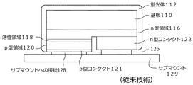
活性領域118がn型領域116の上に形成され、p型領域120が活性領域118の上に形成される。p型領域120、活性領域118及びn型領域116の一部がエッチング除去され、n型領域116の一部を露出する。p型コンタクト121がp型領域120の上に堆積され、n型コンタクト122がn型領域116の露出部の上に堆積される。このLEDが裏返しにされて、ハンダなどの材料126、128により、サブマウント129に取り付けられる。
ができる。ワイヤボンドを形成した後に、カップがシリコーン/蛍光体スラリーで充填される。この構成は、グープインカップ(goop in cup)と呼ばれる。カップ構成内のグープは、低コストであり、製造が容易である。しかしながら、グープインカップ構成は、LEDダイ、ワイヤボンド及び蛍光体/シリコーン材料(グープ)の高い熱抵抗(20C/Wまで高い)のために、大入力電力密度を信頼性をもって扱うことにおいて制限される。フリップチップ型のLEDもまた、カップ構成内のグープ内に配置することができる。フリップチップの利点は、LED及び典型的なフリップチップ相互接続部の熱抵抗が比較的に低い(典型的には<5C/W)ことである。しかしながら、蛍光体/シリコーンの熱抵抗は依然として高く、結果としてデバイスは大電力密度を信頼性をもって扱うことはできない。
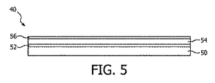
開放層56及びモールディング材料が都合良く選択され、それにより開放層56がLEDの底部表面上の金属に良好に接着するが、モールディング材料には比較的に弱く接着する。モールディング後に、LEDを開放層から容易に除去することができる。
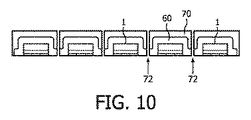
できる。LEDをテストすることができ、そしてユーザーによるPCボードなどの構造への取り付けのための用意が整う。例えば、LED1の底部上の相互接続部26及び28を通じた、ハンダその他の適切な取付技法によって、LEDを他の構造上に取り付ける。
Claims (18)
- 構造体であって:
複数の発光デバイスであり、前記複数の発光デバイスの各々が、第1表面と、前記第1表面に対向する第2表面と、前記第1表面及び前記第2表面を接続する少なくとも1つの側部表面とを有する、複数の発光デバイスと;
前記複数の発光デバイスの各々の前記第1表面に直接接触して配置される波長変換層と;
前記波長変換層に直接接触して配置される光学素子層と;
を含み、
前記複数の発光デバイスが、前記波長変換層及び前記光学素子層を通じてのみ、互いに機械的に接続されている、
構造体。 - 請求項1に記載の構造体であり、
前記波長変換層が、波長変換材料、接着材料及び透明材料の混合物を含む、
構造体。 - 請求項2に記載の構造体であり、
前記透明材料が、少なくとも0.2W/mKの熱伝導性を有する、
構造体。 - 請求項3に記載の構造体であり、
前記透明材料が、少なくとも0.5W/mKの熱伝導性を有する、
構造体。 - 請求項2に記載の構造体であり、
前記透明材料の重量が、前記波長変換層の重量の少なくとも50%である、
構造体。 - 請求項2に記載の構造体であり、
前記接着材料が、前記波長変換層の重量の15%以下の重量を有する、
構造体。 - 請求項2に記載の構造体であり、
前記透明材料が、少なくとも0.2W/mKの熱伝導性を有し、
前記透明材料の重量が、前記波長変換層の重量の少なくとも50%である、
構造体。 - 請求項7に記載の構造体であり、
前記透明材料が、少なくとも0.5W/mKの熱伝導性を有する、
構造体。 - 請求項1に記載の構造体であり、
前記光学素子層が、接着材料及び透明材料の混合物を含む、
構造体。 - 請求項9に記載の構造体であり、
前記透明材料が、少なくとも0.2W/mKの熱伝導性を有する、
構造体。 - 請求項10に記載の構造体であり、
前記光学素子層が、少なくとも0.5W/mKの熱伝導性を有する、
構造体。 - 請求項10に記載の構造体であり、
前記透明材料の重量が、前記波長変換層の重量の少なくとも50%である、
構造体。 - 請求項9に記載の構造体であり、
前記接着材料が、前記波長変換層の重量の15%未満の重量を有する、
構造体。 - 請求項9に記載の構造体であり、
前記透明材料が、少なくとも0.2W/mKの熱伝導性を有し、
前記透明材料の重量が、前記波長変換層の重量の少なくとも50%であり、
前記接着材料の重量が、前記波長変換層の重量の少なくとも0%であり、15%未満である、
構造体。 - 請求項14に記載の構造体であり、
前記光学素子層が、少なくとも0.5W/mKの熱伝導性を有する、
構造体。 - 請求項1に記載の構造体であり、
前記波長変換層の厚さが、0μmを越え100μm未満である、
構造体。 - 請求項1に記載の構造体であり、
前記波長変換層が、隣接する発光デバイスの間の空間において形成されたへこみを含み、前記光学素子層が前記波長変換層のへこみを充填している、
構造体。 - 請求項1に記載の構造体であり、
前記波長変換層が、各前記発光デバイスの前記第2表面以外の全ての表面に配置されている、
構造体。
Applications Claiming Priority (3)
| Application Number | Priority Date | Filing Date | Title |
|---|---|---|---|
| US201462016708P | 2014-06-25 | 2014-06-25 | |
| US62/016,708 | 2014-06-25 | ||
| PCT/IB2015/054700 WO2015198220A1 (en) | 2014-06-25 | 2015-06-23 | Packaged wavelength converted light emitting device |
Related Child Applications (1)
| Application Number | Title | Priority Date | Filing Date |
|---|---|---|---|
| JP2020082366A Division JP7086133B2 (ja) | 2014-06-25 | 2020-05-08 | 波長変換発光デバイス |
Publications (3)
| Publication Number | Publication Date |
|---|---|
| JP2017520926A JP2017520926A (ja) | 2017-07-27 |
| JP2017520926A5 JP2017520926A5 (ja) | 2018-08-09 |
| JP6703494B2 true JP6703494B2 (ja) | 2020-06-03 |
Family
ID=53718057
Family Applications (2)
| Application Number | Title | Priority Date | Filing Date |
|---|---|---|---|
| JP2016575094A Active JP6703494B2 (ja) | 2014-06-25 | 2015-06-23 | パッケージングされた波長変換発光デバイス |
| JP2020082366A Active JP7086133B2 (ja) | 2014-06-25 | 2020-05-08 | 波長変換発光デバイス |
Family Applications After (1)
| Application Number | Title | Priority Date | Filing Date |
|---|---|---|---|
| JP2020082366A Active JP7086133B2 (ja) | 2014-06-25 | 2020-05-08 | 波長変換発光デバイス |
Country Status (7)
| Country | Link |
|---|---|
| US (1) | US10998473B2 (ja) |
| EP (1) | EP3161880B1 (ja) |
| JP (2) | JP6703494B2 (ja) |
| KR (1) | KR102467614B1 (ja) |
| CN (1) | CN106415863A (ja) |
| TW (1) | TW201616689A (ja) |
| WO (1) | WO2015198220A1 (ja) |
Families Citing this family (14)
| Publication number | Priority date | Publication date | Assignee | Title |
|---|---|---|---|---|
| US8384105B2 (en) * | 2010-03-19 | 2013-02-26 | Micron Technology, Inc. | Light emitting diodes with enhanced thermal sinking and associated methods of operation |
| DE102015102460A1 (de) * | 2015-02-20 | 2016-08-25 | Osram Opto Semiconductors Gmbh | Verfahren zur Herstellung eines lichtemittierenden Bauteils und lichtemittierendes Bauteil |
| KR102417181B1 (ko) * | 2015-11-09 | 2022-07-05 | 삼성전자주식회사 | 발광 패키지, 반도체 발광 소자, 발광 모듈 및 발광 패키지의 제조 방법 |
| US10797209B2 (en) | 2016-02-05 | 2020-10-06 | Maven Optronics Co., Ltd. | Light emitting device with beam shaping structure and manufacturing method of the same |
| TWI583028B (zh) * | 2016-02-05 | 2017-05-11 | 行家光電股份有限公司 | 具有光形調整結構之發光裝置及其製造方法 |
| JP6928437B2 (ja) * | 2016-03-04 | 2021-09-01 | 日東電工(上海松江)有限公司 | 封止光半導体素子の製造方法 |
| CN107154453B (zh) * | 2016-03-04 | 2021-11-16 | 日东电工(上海松江)有限公司 | 元件集合体临时固定片及其制造方法 |
| JP6940740B2 (ja) * | 2016-05-06 | 2021-09-29 | 日亜化学工業株式会社 | 発光装置の製造方法 |
| US20170345983A1 (en) * | 2016-05-26 | 2017-11-30 | Epistar Corporation | Light-emitting device and light-emitting apparatus comprising the same |
| CN105957943A (zh) * | 2016-06-17 | 2016-09-21 | 深圳市兆驰节能照明股份有限公司 | 芯片级封装发光装置及其制造方法 |
| CN105938869A (zh) * | 2016-06-21 | 2016-09-14 | 深圳市兆驰节能照明股份有限公司 | 双层结构芯片级封装光源及其制造方法 |
| US11637225B2 (en) | 2017-12-20 | 2023-04-25 | Lumileds Llc | Converter with glass layers |
| EP3729526A1 (en) * | 2017-12-22 | 2020-10-28 | Lumileds LLC | Porous micron-sized particles to tune light scattering |
| WO2023091698A1 (en) * | 2021-11-18 | 2023-05-25 | Lumileds Llc | Light-emitting diode (led) package with reflective coating and method of manufacture |
Family Cites Families (39)
| Publication number | Priority date | Publication date | Assignee | Title |
|---|---|---|---|---|
| JP3589187B2 (ja) * | 2000-07-31 | 2004-11-17 | 日亜化学工業株式会社 | 発光装置の形成方法 |
| DE10156386B4 (de) * | 2001-11-16 | 2007-08-09 | Infineon Technologies Ag | Verfahren zum Herstellen eines Halbleiterchips |
| US6870311B2 (en) * | 2002-06-07 | 2005-03-22 | Lumileds Lighting U.S., Llc | Light-emitting devices utilizing nanoparticles |
| JP2005252219A (ja) * | 2004-02-06 | 2005-09-15 | Toyoda Gosei Co Ltd | 発光装置及び封止部材 |
| JP4348267B2 (ja) | 2004-09-22 | 2009-10-21 | シャープ株式会社 | 光半導体装置、光通信装置および電子機器 |
| TWI280673B (en) | 2004-09-22 | 2007-05-01 | Sharp Kk | Optical semiconductor device, optical communication device, and electronic equipment |
| EP1919000A1 (en) | 2005-08-05 | 2008-05-07 | Matsushita Electric Industries Co., Ltd. | Semiconductor light-emitting device |
| CN101208811A (zh) | 2005-08-05 | 2008-06-25 | 松下电器产业株式会社 | 半导体发光装置 |
| JP2007243056A (ja) * | 2006-03-10 | 2007-09-20 | Matsushita Electric Works Ltd | 発光装置 |
| US20070215998A1 (en) | 2006-03-20 | 2007-09-20 | Chi Lin Technology Co., Ltd. | LED package structure and method for manufacturing the same |
| US7842960B2 (en) * | 2006-09-06 | 2010-11-30 | Lumination Llc | Light emitting packages and methods of making same |
| JP5578597B2 (ja) * | 2007-09-03 | 2014-08-27 | 独立行政法人物質・材料研究機構 | 蛍光体及びその製造方法、並びにそれを用いた発光装置 |
| DE102009018087A1 (de) | 2008-04-30 | 2009-12-17 | Ledon Lighting Jennersdorf Gmbh | Lichtemittierende Diode mit erhöhter Farbstabilität |
| JP2010103522A (ja) * | 2008-10-21 | 2010-05-06 | Seoul Opto Devices Co Ltd | 遅延蛍光体を備える交流駆動型の発光素子及び発光素子モジュール |
| JP4724222B2 (ja) * | 2008-12-12 | 2011-07-13 | 株式会社東芝 | 発光装置の製造方法 |
| US8507300B2 (en) * | 2008-12-24 | 2013-08-13 | Ledengin, Inc. | Light-emitting diode with light-conversion layer |
| US20110012147A1 (en) | 2009-07-15 | 2011-01-20 | Koninklijke Philips Electronics N.V. | Wavelength-converted semiconductor light emitting device including a filter and a scattering structure |
| DE102009036621B4 (de) | 2009-08-07 | 2023-12-21 | OSRAM Opto Semiconductors Gesellschaft mit beschränkter Haftung | Optoelektronisches Halbleiterbauteil |
| US8203161B2 (en) * | 2009-11-23 | 2012-06-19 | Koninklijke Philips Electronics N.V. | Wavelength converted semiconductor light emitting device |
| US8329482B2 (en) * | 2010-04-30 | 2012-12-11 | Cree, Inc. | White-emitting LED chips and method for making same |
| JP5468985B2 (ja) * | 2010-05-17 | 2014-04-09 | 株式会社小糸製作所 | 照明装置 |
| CN103003966B (zh) | 2010-05-18 | 2016-08-10 | 首尔半导体株式会社 | 具有波长变换层的发光二级管芯片及其制造方法,以及包括其的封装件及其制造方法 |
| WO2011145794A1 (ko) * | 2010-05-18 | 2011-11-24 | 서울반도체 주식회사 | 파장변환층을 갖는 발광 다이오드 칩과 그 제조 방법, 및 그것을 포함하는 패키지 및 그 제조 방법 |
| JP5390472B2 (ja) * | 2010-06-03 | 2014-01-15 | 株式会社東芝 | 半導体発光装置及びその製造方法 |
| JP5511524B2 (ja) * | 2010-06-07 | 2014-06-04 | 日東電工株式会社 | 光半導体用封止シート |
| JP2012019062A (ja) * | 2010-07-08 | 2012-01-26 | Shin Etsu Chem Co Ltd | 発光半導体装置、実装基板及びそれらの製造方法 |
| DE102010034913B4 (de) * | 2010-08-20 | 2023-03-30 | OSRAM Opto Semiconductors Gesellschaft mit beschränkter Haftung | Strahlung emittierendes Bauelement und Verfahren zur Herstellung des Strahlung emittierenden Bauelements |
| SG190320A1 (en) * | 2010-12-13 | 2013-07-31 | Toray Industries | Phosphor sheet, led and light emitting device using same and method for producing led |
| JP5619680B2 (ja) * | 2011-06-03 | 2014-11-05 | シチズンホールディングス株式会社 | 半導体発光素子の製造方法 |
| JPWO2013011628A1 (ja) | 2011-07-19 | 2015-02-23 | パナソニック株式会社 | 発光装置及びその製造方法 |
| WO2013066920A2 (en) * | 2011-11-03 | 2013-05-10 | Cooledge Lighting, Inc. | Broad-area lighting systems |
| WO2013112435A1 (en) * | 2012-01-24 | 2013-08-01 | Cooledge Lighting Inc. | Light - emitting devices having discrete phosphor chips and fabrication methods |
| US8957429B2 (en) | 2012-02-07 | 2015-02-17 | Epistar Corporation | Light emitting diode with wavelength conversion layer |
| CN103311380A (zh) | 2012-03-08 | 2013-09-18 | 展晶科技(深圳)有限公司 | 半导体封装制程及其封装结构 |
| KR101291092B1 (ko) * | 2012-04-06 | 2013-08-01 | 주식회사 씨티랩 | 반도체 소자 구조물을 제조하는 방법 |
| US8889439B2 (en) * | 2012-08-24 | 2014-11-18 | Tsmc Solid State Lighting Ltd. | Method and apparatus for packaging phosphor-coated LEDs |
| DE102012113003A1 (de) | 2012-12-21 | 2014-04-03 | Osram Opto Semiconductors Gmbh | Verfahren zur Herstellung eines optoelektronischen Halbleiterbauteils und optoelektronisches Halbleiterbauteil |
| DE102013103416A1 (de) * | 2013-04-05 | 2014-10-23 | Osram Opto Semiconductors Gmbh | Elektromagnetische Strahlung emittierende Baugruppe und Verfahren zum Herstellen einer elektromagnetische Strahlung emittierenden Baugruppe |
| KR102071463B1 (ko) * | 2013-04-08 | 2020-01-30 | 루미리즈 홀딩 비.브이. | 형광체 변환 층에 높은 열 전도도 입자를 갖는 led 및 그 제조 방법 |
-
2015
- 2015-06-22 TW TW104120031A patent/TW201616689A/zh unknown
- 2015-06-23 CN CN201580034191.6A patent/CN106415863A/zh active Pending
- 2015-06-23 WO PCT/IB2015/054700 patent/WO2015198220A1/en active Application Filing
- 2015-06-23 EP EP15741340.2A patent/EP3161880B1/en active Active
- 2015-06-23 JP JP2016575094A patent/JP6703494B2/ja active Active
- 2015-06-23 US US15/319,095 patent/US10998473B2/en active Active
- 2015-06-23 KR KR1020177002103A patent/KR102467614B1/ko active IP Right Grant
-
2020
- 2020-05-08 JP JP2020082366A patent/JP7086133B2/ja active Active
Also Published As
| Publication number | Publication date |
|---|---|
| JP7086133B2 (ja) | 2022-06-17 |
| US10998473B2 (en) | 2021-05-04 |
| CN106415863A (zh) | 2017-02-15 |
| JP2020145453A (ja) | 2020-09-10 |
| EP3161880B1 (en) | 2022-06-29 |
| EP3161880A1 (en) | 2017-05-03 |
| US20170133560A1 (en) | 2017-05-11 |
| WO2015198220A1 (en) | 2015-12-30 |
| KR20170020914A (ko) | 2017-02-24 |
| TW201616689A (zh) | 2016-05-01 |
| KR102467614B1 (ko) | 2022-11-16 |
| JP2017520926A (ja) | 2017-07-27 |
Similar Documents
| Publication | Publication Date | Title |
|---|---|---|
| JP7086133B2 (ja) | 波長変換発光デバイス | |
| KR102245056B1 (ko) | 전면 발광형 반도체 발광 장치 | |
| US10886440B2 (en) | Wavelength converted semiconductor light emitting device | |
| KR102237304B1 (ko) | 반사기 및 광학 요소를 갖는 발광 디바이스 | |
| JP6535598B2 (ja) | フィルタ及び保護層を含む発光デバイス | |
| JP6552473B2 (ja) | 厚い金属層を有する半導体発光デバイス | |
| JP7361810B2 (ja) | 反射層を伴うマウント上の発光デバイス | |
| JP6100794B2 (ja) | 厚い金属層を有する半導体発光デバイス | |
| KR102504008B1 (ko) | 다수의 적층된 발광 디바이스를 갖는 디바이스 |
Legal Events
| Date | Code | Title | Description |
|---|---|---|---|
| A521 | Request for written amendment filed |
Free format text: JAPANESE INTERMEDIATE CODE: A523 Effective date: 20170223 |
|
| A521 | Request for written amendment filed |
Free format text: JAPANESE INTERMEDIATE CODE: A523 Effective date: 20180625 |
|
| A621 | Written request for application examination |
Free format text: JAPANESE INTERMEDIATE CODE: A621 Effective date: 20180625 |
|
| A711 | Notification of change in applicant |
Free format text: JAPANESE INTERMEDIATE CODE: A711 Effective date: 20190307 |
|
| A977 | Report on retrieval |
Free format text: JAPANESE INTERMEDIATE CODE: A971007 Effective date: 20190424 |
|
| A131 | Notification of reasons for refusal |
Free format text: JAPANESE INTERMEDIATE CODE: A131 Effective date: 20190507 |
|
| A521 | Request for written amendment filed |
Free format text: JAPANESE INTERMEDIATE CODE: A523 Effective date: 20190805 |
|
| A131 | Notification of reasons for refusal |
Free format text: JAPANESE INTERMEDIATE CODE: A131 Effective date: 20191023 |
|
| TRDD | Decision of grant or rejection written | ||
| A01 | Written decision to grant a patent or to grant a registration (utility model) |
Free format text: JAPANESE INTERMEDIATE CODE: A01 Effective date: 20200317 |
|
| A601 | Written request for extension of time |
Free format text: JAPANESE INTERMEDIATE CODE: A601 Effective date: 20200414 |
|
| A61 | First payment of annual fees (during grant procedure) |
Free format text: JAPANESE INTERMEDIATE CODE: A61 Effective date: 20200508 |
|
| R150 | Certificate of patent or registration of utility model |
Ref document number: 6703494 Country of ref document: JP Free format text: JAPANESE INTERMEDIATE CODE: R150 |
|
| R250 | Receipt of annual fees |
Free format text: JAPANESE INTERMEDIATE CODE: R250 |