JP6672301B2 - 簡易に製造可能な電気部品及び電気部品の製造方法 - Google Patents
簡易に製造可能な電気部品及び電気部品の製造方法 Download PDFInfo
- Publication number
- JP6672301B2 JP6672301B2 JP2017530257A JP2017530257A JP6672301B2 JP 6672301 B2 JP6672301 B2 JP 6672301B2 JP 2017530257 A JP2017530257 A JP 2017530257A JP 2017530257 A JP2017530257 A JP 2017530257A JP 6672301 B2 JP6672301 B2 JP 6672301B2
- Authority
- JP
- Japan
- Prior art keywords
- chip
- support substrate
- substrate
- polymer layer
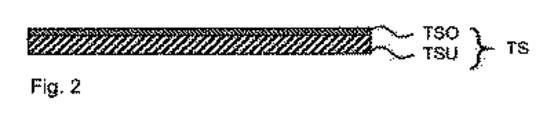
- tso
- Prior art date
- Legal status (The legal status is an assumption and is not a legal conclusion. Google has not performed a legal analysis and makes no representation as to the accuracy of the status listed.)
- Active
Links
- 238000000034 method Methods 0.000 title claims description 28
- 238000004519 manufacturing process Methods 0.000 title claims description 15
- 239000000758 substrate Substances 0.000 claims description 174
- 229920000642 polymer Polymers 0.000 claims description 76
- 229910052751 metal Inorganic materials 0.000 claims description 46
- 239000002184 metal Substances 0.000 claims description 46
- 239000000463 material Substances 0.000 claims description 20
- 239000000945 filler Substances 0.000 claims description 16
- 239000011796 hollow space material Substances 0.000 claims description 16
- 238000005304 joining Methods 0.000 claims description 16
- 239000004020 conductor Substances 0.000 claims description 11
- 229910052802 copper Inorganic materials 0.000 claims description 8
- 239000004065 semiconductor Substances 0.000 claims description 7
- 229910052782 aluminium Inorganic materials 0.000 claims description 6
- 230000000149 penetrating effect Effects 0.000 claims description 6
- 229910052709 silver Inorganic materials 0.000 claims description 6
- 239000000919 ceramic Substances 0.000 claims description 5
- 238000007639 printing Methods 0.000 claims description 5
- 238000010438 heat treatment Methods 0.000 claims description 4
- 239000000956 alloy Substances 0.000 claims description 3
- 229910045601 alloy Inorganic materials 0.000 claims description 3
- 239000013078 crystal Substances 0.000 claims description 3
- 238000000151 deposition Methods 0.000 claims description 3
- 239000011521 glass Substances 0.000 claims description 3
- 239000002105 nanoparticle Substances 0.000 claims description 3
- 230000005693 optoelectronics Effects 0.000 claims description 3
- 238000005507 spraying Methods 0.000 claims description 3
- SWPMTVXRLXPNDP-UHFFFAOYSA-N 4-hydroxy-2,6,6-trimethylcyclohexene-1-carbaldehyde Chemical compound CC1=C(C=O)C(C)(C)CC(O)C1 SWPMTVXRLXPNDP-UHFFFAOYSA-N 0.000 claims 1
- 101100460147 Sarcophaga bullata NEMS gene Proteins 0.000 claims 1
- 230000003287 optical effect Effects 0.000 claims 1
- PXHVJJICTQNCMI-UHFFFAOYSA-N Nickel Chemical compound [Ni] PXHVJJICTQNCMI-UHFFFAOYSA-N 0.000 description 10
- 239000010949 copper Substances 0.000 description 9
- 239000002131 composite material Substances 0.000 description 5
- 239000010931 gold Substances 0.000 description 5
- 229910052759 nickel Inorganic materials 0.000 description 5
- 239000012778 molding material Substances 0.000 description 4
- 239000011248 coating agent Substances 0.000 description 3
- 238000000576 coating method Methods 0.000 description 3
- 230000000694 effects Effects 0.000 description 3
- 238000009429 electrical wiring Methods 0.000 description 3
- 150000002739 metals Chemical class 0.000 description 3
- RYGMFSIKBFXOCR-UHFFFAOYSA-N Copper Chemical compound [Cu] RYGMFSIKBFXOCR-UHFFFAOYSA-N 0.000 description 2
- XEEYBQQBJWHFJM-UHFFFAOYSA-N Iron Chemical compound [Fe] XEEYBQQBJWHFJM-UHFFFAOYSA-N 0.000 description 2
- 238000005452 bending Methods 0.000 description 2
- 239000007788 liquid Substances 0.000 description 2
- 238000001459 lithography Methods 0.000 description 2
- 239000002082 metal nanoparticle Substances 0.000 description 2
- 238000000465 moulding Methods 0.000 description 2
- 239000002861 polymer material Substances 0.000 description 2
- 230000001681 protective effect Effects 0.000 description 2
- 230000035945 sensitivity Effects 0.000 description 2
- 125000006850 spacer group Chemical group 0.000 description 2
- 238000010897 surface acoustic wave method Methods 0.000 description 2
- 241000446313 Lamella Species 0.000 description 1
- 230000002411 adverse Effects 0.000 description 1
- XAGFODPZIPBFFR-UHFFFAOYSA-N aluminium Chemical compound [Al] XAGFODPZIPBFFR-UHFFFAOYSA-N 0.000 description 1
- 230000004888 barrier function Effects 0.000 description 1
- 230000003796 beauty Effects 0.000 description 1
- 230000007547 defect Effects 0.000 description 1
- 230000002950 deficient Effects 0.000 description 1
- 230000001419 dependent effect Effects 0.000 description 1
- 238000007772 electroless plating Methods 0.000 description 1
- 238000009713 electroplating Methods 0.000 description 1
- 238000005516 engineering process Methods 0.000 description 1
- 238000011156 evaluation Methods 0.000 description 1
- PCHJSUWPFVWCPO-UHFFFAOYSA-N gold Chemical compound [Au] PCHJSUWPFVWCPO-UHFFFAOYSA-N 0.000 description 1
- 229910052737 gold Inorganic materials 0.000 description 1
- 230000001771 impaired effect Effects 0.000 description 1
- 238000003780 insertion Methods 0.000 description 1
- 230000037431 insertion Effects 0.000 description 1
- 230000002452 interceptive effect Effects 0.000 description 1
- 229910052742 iron Inorganic materials 0.000 description 1
- 238000001465 metallisation Methods 0.000 description 1
- 239000000203 mixture Substances 0.000 description 1
- 230000001590 oxidative effect Effects 0.000 description 1
- 239000002245 particle Substances 0.000 description 1
- 238000007789 sealing Methods 0.000 description 1
- 239000004332 silver Substances 0.000 description 1
- 229910000679 solder Inorganic materials 0.000 description 1
- 238000005476 soldering Methods 0.000 description 1
- 229920003002 synthetic resin Polymers 0.000 description 1
- 239000000057 synthetic resin Substances 0.000 description 1
- 239000010409 thin film Substances 0.000 description 1
Images


Classifications
-
- H—ELECTRICITY
- H04—ELECTRIC COMMUNICATION TECHNIQUE
- H04R—LOUDSPEAKERS, MICROPHONES, GRAMOPHONE PICK-UPS OR LIKE ACOUSTIC ELECTROMECHANICAL TRANSDUCERS; DEAF-AID SETS; PUBLIC ADDRESS SYSTEMS
- H04R1/00—Details of transducers, loudspeakers or microphones
- H04R1/20—Arrangements for obtaining desired frequency or directional characteristics
- H04R1/22—Arrangements for obtaining desired frequency or directional characteristics for obtaining desired frequency characteristic only
- H04R1/222—Arrangements for obtaining desired frequency or directional characteristics for obtaining desired frequency characteristic only for microphones
-
- B—PERFORMING OPERATIONS; TRANSPORTING
- B81—MICROSTRUCTURAL TECHNOLOGY
- B81B—MICROSTRUCTURAL DEVICES OR SYSTEMS, e.g. MICROMECHANICAL DEVICES
- B81B7/00—Microstructural systems; Auxiliary parts of microstructural devices or systems
- B81B7/0032—Packages or encapsulation
- B81B7/0061—Packages or encapsulation suitable for fluid transfer from the MEMS out of the package or vice versa, e.g. transfer of liquid, gas, sound
-
- B—PERFORMING OPERATIONS; TRANSPORTING
- B81—MICROSTRUCTURAL TECHNOLOGY
- B81C—PROCESSES OR APPARATUS SPECIALLY ADAPTED FOR THE MANUFACTURE OR TREATMENT OF MICROSTRUCTURAL DEVICES OR SYSTEMS
- B81C1/00—Manufacture or treatment of devices or systems in or on a substrate
- B81C1/00015—Manufacture or treatment of devices or systems in or on a substrate for manufacturing microsystems
- B81C1/00222—Integrating an electronic processing unit with a micromechanical structure
- B81C1/0023—Packaging together an electronic processing unit die and a micromechanical structure die
-
- H—ELECTRICITY
- H01—ELECTRIC ELEMENTS
- H01L—SEMICONDUCTOR DEVICES NOT COVERED BY CLASS H10
- H01L24/00—Arrangements for connecting or disconnecting semiconductor or solid-state bodies; Methods or apparatus related thereto
- H01L24/01—Means for bonding being attached to, or being formed on, the surface to be connected, e.g. chip-to-package, die-attach, "first-level" interconnects; Manufacturing methods related thereto
- H01L24/18—High density interconnect [HDI] connectors; Manufacturing methods related thereto
- H01L24/19—Manufacturing methods of high density interconnect preforms
-
- H—ELECTRICITY
- H01—ELECTRIC ELEMENTS
- H01L—SEMICONDUCTOR DEVICES NOT COVERED BY CLASS H10
- H01L24/00—Arrangements for connecting or disconnecting semiconductor or solid-state bodies; Methods or apparatus related thereto
- H01L24/01—Means for bonding being attached to, or being formed on, the surface to be connected, e.g. chip-to-package, die-attach, "first-level" interconnects; Manufacturing methods related thereto
- H01L24/18—High density interconnect [HDI] connectors; Manufacturing methods related thereto
- H01L24/20—Structure, shape, material or disposition of high density interconnect preforms
-
- H—ELECTRICITY
- H01—ELECTRIC ELEMENTS
- H01L—SEMICONDUCTOR DEVICES NOT COVERED BY CLASS H10
- H01L24/00—Arrangements for connecting or disconnecting semiconductor or solid-state bodies; Methods or apparatus related thereto
- H01L24/93—Batch processes
- H01L24/95—Batch processes at chip-level, i.e. with connecting carried out on a plurality of singulated devices, i.e. on diced chips
- H01L24/97—Batch processes at chip-level, i.e. with connecting carried out on a plurality of singulated devices, i.e. on diced chips the devices being connected to a common substrate, e.g. interposer, said common substrate being separable into individual assemblies after connecting
-
- H—ELECTRICITY
- H03—ELECTRONIC CIRCUITRY
- H03H—IMPEDANCE NETWORKS, e.g. RESONANT CIRCUITS; RESONATORS
- H03H9/00—Networks comprising electromechanical or electro-acoustic devices; Electromechanical resonators
- H03H9/02—Details
- H03H9/05—Holders; Supports
- H03H9/0504—Holders; Supports for bulk acoustic wave devices
- H03H9/0514—Holders; Supports for bulk acoustic wave devices consisting of mounting pads or bumps
- H03H9/0523—Holders; Supports for bulk acoustic wave devices consisting of mounting pads or bumps for flip-chip mounting
-
- H—ELECTRICITY
- H03—ELECTRONIC CIRCUITRY
- H03H—IMPEDANCE NETWORKS, e.g. RESONANT CIRCUITS; RESONATORS
- H03H9/00—Networks comprising electromechanical or electro-acoustic devices; Electromechanical resonators
- H03H9/02—Details
- H03H9/05—Holders; Supports
- H03H9/058—Holders; Supports for surface acoustic wave devices
-
- H—ELECTRICITY
- H04—ELECTRIC COMMUNICATION TECHNIQUE
- H04R—LOUDSPEAKERS, MICROPHONES, GRAMOPHONE PICK-UPS OR LIKE ACOUSTIC ELECTROMECHANICAL TRANSDUCERS; DEAF-AID SETS; PUBLIC ADDRESS SYSTEMS
- H04R1/00—Details of transducers, loudspeakers or microphones
- H04R1/02—Casings; Cabinets ; Supports therefor; Mountings therein
-
- H—ELECTRICITY
- H04—ELECTRIC COMMUNICATION TECHNIQUE
- H04R—LOUDSPEAKERS, MICROPHONES, GRAMOPHONE PICK-UPS OR LIKE ACOUSTIC ELECTROMECHANICAL TRANSDUCERS; DEAF-AID SETS; PUBLIC ADDRESS SYSTEMS
- H04R1/00—Details of transducers, loudspeakers or microphones
- H04R1/06—Arranging circuit leads; Relieving strain on circuit leads
-
- H—ELECTRICITY
- H04—ELECTRIC COMMUNICATION TECHNIQUE
- H04R—LOUDSPEAKERS, MICROPHONES, GRAMOPHONE PICK-UPS OR LIKE ACOUSTIC ELECTROMECHANICAL TRANSDUCERS; DEAF-AID SETS; PUBLIC ADDRESS SYSTEMS
- H04R19/00—Electrostatic transducers
- H04R19/005—Electrostatic transducers using semiconductor materials
-
- H—ELECTRICITY
- H04—ELECTRIC COMMUNICATION TECHNIQUE
- H04R—LOUDSPEAKERS, MICROPHONES, GRAMOPHONE PICK-UPS OR LIKE ACOUSTIC ELECTROMECHANICAL TRANSDUCERS; DEAF-AID SETS; PUBLIC ADDRESS SYSTEMS
- H04R19/00—Electrostatic transducers
- H04R19/04—Microphones
-
- H—ELECTRICITY
- H04—ELECTRIC COMMUNICATION TECHNIQUE
- H04R—LOUDSPEAKERS, MICROPHONES, GRAMOPHONE PICK-UPS OR LIKE ACOUSTIC ELECTROMECHANICAL TRANSDUCERS; DEAF-AID SETS; PUBLIC ADDRESS SYSTEMS
- H04R23/00—Transducers other than those covered by groups H04R9/00 - H04R21/00
- H04R23/02—Transducers using more than one principle simultaneously
-
- H—ELECTRICITY
- H04—ELECTRIC COMMUNICATION TECHNIQUE
- H04R—LOUDSPEAKERS, MICROPHONES, GRAMOPHONE PICK-UPS OR LIKE ACOUSTIC ELECTROMECHANICAL TRANSDUCERS; DEAF-AID SETS; PUBLIC ADDRESS SYSTEMS
- H04R3/00—Circuits for transducers, loudspeakers or microphones
- H04R3/007—Protection circuits for transducers
-
- H—ELECTRICITY
- H04—ELECTRIC COMMUNICATION TECHNIQUE
- H04R—LOUDSPEAKERS, MICROPHONES, GRAMOPHONE PICK-UPS OR LIKE ACOUSTIC ELECTROMECHANICAL TRANSDUCERS; DEAF-AID SETS; PUBLIC ADDRESS SYSTEMS
- H04R31/00—Apparatus or processes specially adapted for the manufacture of transducers or diaphragms therefor
-
- B—PERFORMING OPERATIONS; TRANSPORTING
- B81—MICROSTRUCTURAL TECHNOLOGY
- B81B—MICROSTRUCTURAL DEVICES OR SYSTEMS, e.g. MICROMECHANICAL DEVICES
- B81B2201/00—Specific applications of microelectromechanical systems
- B81B2201/02—Sensors
- B81B2201/0257—Microphones or microspeakers
-
- B—PERFORMING OPERATIONS; TRANSPORTING
- B81—MICROSTRUCTURAL TECHNOLOGY
- B81B—MICROSTRUCTURAL DEVICES OR SYSTEMS, e.g. MICROMECHANICAL DEVICES
- B81B2207/00—Microstructural systems or auxiliary parts thereof
- B81B2207/01—Microstructural systems or auxiliary parts thereof comprising a micromechanical device connected to control or processing electronics, i.e. Smart-MEMS
- B81B2207/012—Microstructural systems or auxiliary parts thereof comprising a micromechanical device connected to control or processing electronics, i.e. Smart-MEMS the micromechanical device and the control or processing electronics being separate parts in the same package
-
- B—PERFORMING OPERATIONS; TRANSPORTING
- B81—MICROSTRUCTURAL TECHNOLOGY
- B81B—MICROSTRUCTURAL DEVICES OR SYSTEMS, e.g. MICROMECHANICAL DEVICES
- B81B2207/00—Microstructural systems or auxiliary parts thereof
- B81B2207/09—Packages
- B81B2207/091—Arrangements for connecting external electrical signals to mechanical structures inside the package
- B81B2207/098—Arrangements not provided for in groups B81B2207/092 - B81B2207/097
-
- H—ELECTRICITY
- H01—ELECTRIC ELEMENTS
- H01L—SEMICONDUCTOR DEVICES NOT COVERED BY CLASS H10
- H01L21/00—Processes or apparatus adapted for the manufacture or treatment of semiconductor or solid state devices or of parts thereof
- H01L21/02—Manufacture or treatment of semiconductor devices or of parts thereof
- H01L21/04—Manufacture or treatment of semiconductor devices or of parts thereof the devices having at least one potential-jump barrier or surface barrier, e.g. PN junction, depletion layer or carrier concentration layer
- H01L21/50—Assembly of semiconductor devices using processes or apparatus not provided for in a single one of the subgroups H01L21/06 - H01L21/326, e.g. sealing of a cap to a base of a container
- H01L21/56—Encapsulations, e.g. encapsulation layers, coatings
- H01L21/568—Temporary substrate used as encapsulation process aid
-
- H—ELECTRICITY
- H01—ELECTRIC ELEMENTS
- H01L—SEMICONDUCTOR DEVICES NOT COVERED BY CLASS H10
- H01L2224/00—Indexing scheme for arrangements for connecting or disconnecting semiconductor or solid-state bodies and methods related thereto as covered by H01L24/00
- H01L2224/01—Means for bonding being attached to, or being formed on, the surface to be connected, e.g. chip-to-package, die-attach, "first-level" interconnects; Manufacturing methods related thereto
- H01L2224/02—Bonding areas; Manufacturing methods related thereto
- H01L2224/04—Structure, shape, material or disposition of the bonding areas prior to the connecting process
- H01L2224/04105—Bonding areas formed on an encapsulation of the semiconductor or solid-state body, e.g. bonding areas on chip-scale packages
-
- H—ELECTRICITY
- H01—ELECTRIC ELEMENTS
- H01L—SEMICONDUCTOR DEVICES NOT COVERED BY CLASS H10
- H01L2224/00—Indexing scheme for arrangements for connecting or disconnecting semiconductor or solid-state bodies and methods related thereto as covered by H01L24/00
- H01L2224/01—Means for bonding being attached to, or being formed on, the surface to be connected, e.g. chip-to-package, die-attach, "first-level" interconnects; Manufacturing methods related thereto
- H01L2224/18—High density interconnect [HDI] connectors; Manufacturing methods related thereto
- H01L2224/23—Structure, shape, material or disposition of the high density interconnect connectors after the connecting process
- H01L2224/24—Structure, shape, material or disposition of the high density interconnect connectors after the connecting process of an individual high density interconnect connector
- H01L2224/241—Disposition
- H01L2224/24135—Connecting between different semiconductor or solid-state bodies, i.e. chip-to-chip
- H01L2224/24137—Connecting between different semiconductor or solid-state bodies, i.e. chip-to-chip the bodies being arranged next to each other, e.g. on a common substrate
-
- H—ELECTRICITY
- H01—ELECTRIC ELEMENTS
- H01L—SEMICONDUCTOR DEVICES NOT COVERED BY CLASS H10
- H01L2224/00—Indexing scheme for arrangements for connecting or disconnecting semiconductor or solid-state bodies and methods related thereto as covered by H01L24/00
- H01L2224/01—Means for bonding being attached to, or being formed on, the surface to be connected, e.g. chip-to-package, die-attach, "first-level" interconnects; Manufacturing methods related thereto
- H01L2224/18—High density interconnect [HDI] connectors; Manufacturing methods related thereto
- H01L2224/23—Structure, shape, material or disposition of the high density interconnect connectors after the connecting process
- H01L2224/24—Structure, shape, material or disposition of the high density interconnect connectors after the connecting process of an individual high density interconnect connector
- H01L2224/241—Disposition
- H01L2224/24151—Connecting between a semiconductor or solid-state body and an item not being a semiconductor or solid-state body, e.g. chip-to-substrate, chip-to-passive
- H01L2224/24153—Connecting between a semiconductor or solid-state body and an item not being a semiconductor or solid-state body, e.g. chip-to-substrate, chip-to-passive the body and the item being arranged next to each other, e.g. on a common substrate
- H01L2224/24195—Connecting between a semiconductor or solid-state body and an item not being a semiconductor or solid-state body, e.g. chip-to-substrate, chip-to-passive the body and the item being arranged next to each other, e.g. on a common substrate the item being a discrete passive component
-
- H—ELECTRICITY
- H01—ELECTRIC ELEMENTS
- H01L—SEMICONDUCTOR DEVICES NOT COVERED BY CLASS H10
- H01L2224/00—Indexing scheme for arrangements for connecting or disconnecting semiconductor or solid-state bodies and methods related thereto as covered by H01L24/00
- H01L2224/73—Means for bonding being of different types provided for in two or more of groups H01L2224/10, H01L2224/18, H01L2224/26, H01L2224/34, H01L2224/42, H01L2224/50, H01L2224/63, H01L2224/71
- H01L2224/732—Location after the connecting process
- H01L2224/73201—Location after the connecting process on the same surface
- H01L2224/73217—Layer and HDI connectors
-
- H—ELECTRICITY
- H01—ELECTRIC ELEMENTS
- H01L—SEMICONDUCTOR DEVICES NOT COVERED BY CLASS H10
- H01L2924/00—Indexing scheme for arrangements or methods for connecting or disconnecting semiconductor or solid-state bodies as covered by H01L24/00
- H01L2924/10—Details of semiconductor or other solid state devices to be connected
- H01L2924/11—Device type
- H01L2924/14—Integrated circuits
-
- H—ELECTRICITY
- H01—ELECTRIC ELEMENTS
- H01L—SEMICONDUCTOR DEVICES NOT COVERED BY CLASS H10
- H01L2924/00—Indexing scheme for arrangements or methods for connecting or disconnecting semiconductor or solid-state bodies as covered by H01L24/00
- H01L2924/10—Details of semiconductor or other solid state devices to be connected
- H01L2924/146—Mixed devices
- H01L2924/1461—MEMS
-
- H—ELECTRICITY
- H01—ELECTRIC ELEMENTS
- H01L—SEMICONDUCTOR DEVICES NOT COVERED BY CLASS H10
- H01L2924/00—Indexing scheme for arrangements or methods for connecting or disconnecting semiconductor or solid-state bodies as covered by H01L24/00
- H01L2924/19—Details of hybrid assemblies other than the semiconductor or other solid state devices to be connected
- H01L2924/191—Disposition
- H01L2924/19101—Disposition of discrete passive components
- H01L2924/19105—Disposition of discrete passive components in a side-by-side arrangement on a common die mounting substrate
Applications Claiming Priority (3)
| Application Number | Priority Date | Filing Date | Title |
|---|---|---|---|
| DE102014118214.6A DE102014118214B4 (de) | 2014-12-09 | 2014-12-09 | Einfach herstellbares elektrisches Bauelement und Verfahren zur Herstellung eines elektrischen Bauelements |
| DE102014118214.6 | 2014-12-09 | ||
| PCT/EP2015/074148 WO2016091438A1 (de) | 2014-12-09 | 2015-10-19 | Einfach herstellbares elektrisches bauelement und verfahren zur herstellung eines elektrischen bauelements |
Publications (3)
| Publication Number | Publication Date |
|---|---|
| JP2018506171A JP2018506171A (ja) | 2018-03-01 |
| JP2018506171A5 JP2018506171A5 (de) | 2018-11-08 |
| JP6672301B2 true JP6672301B2 (ja) | 2020-03-25 |
Family
ID=54330770
Family Applications (1)
| Application Number | Title | Priority Date | Filing Date |
|---|---|---|---|
| JP2017530257A Active JP6672301B2 (ja) | 2014-12-09 | 2015-10-19 | 簡易に製造可能な電気部品及び電気部品の製造方法 |
Country Status (10)
| Country | Link |
|---|---|
| US (1) | US11245977B2 (de) |
| EP (1) | EP3231010B1 (de) |
| JP (1) | JP6672301B2 (de) |
| KR (1) | KR102561741B1 (de) |
| CN (1) | CN107004664B (de) |
| BR (1) | BR112017012118A2 (de) |
| DE (1) | DE102014118214B4 (de) |
| ES (1) | ES2873364T3 (de) |
| MX (1) | MX2017007254A (de) |
| WO (1) | WO2016091438A1 (de) |
Families Citing this family (4)
| Publication number | Priority date | Publication date | Assignee | Title |
|---|---|---|---|---|
| US11067768B2 (en) * | 2017-11-16 | 2021-07-20 | Tdk Taiwan Corp. | Optical member driving mechanism |
| CN111003682A (zh) * | 2018-10-08 | 2020-04-14 | 凤凰先驱股份有限公司 | 电子封装件及其制法 |
| CN111821567A (zh) * | 2019-03-30 | 2020-10-27 | 深圳硅基仿生科技有限公司 | 电子封装体及植入式器件 |
| CN111422821A (zh) * | 2020-03-13 | 2020-07-17 | 清华大学 | 微系统封装方法 |
Family Cites Families (28)
| Publication number | Priority date | Publication date | Assignee | Title |
|---|---|---|---|---|
| US7434305B2 (en) | 2000-11-28 | 2008-10-14 | Knowles Electronics, Llc. | Method of manufacturing a microphone |
| DE10164494B9 (de) | 2001-12-28 | 2014-08-21 | Epcos Ag | Verkapseltes Bauelement mit geringer Bauhöhe sowie Verfahren zur Herstellung |
| US6781231B2 (en) * | 2002-09-10 | 2004-08-24 | Knowles Electronics Llc | Microelectromechanical system package with environmental and interference shield |
| JP4484544B2 (ja) | 2004-02-25 | 2010-06-16 | 京セラ株式会社 | 高周波モジュールの製造方法 |
| US7323675B2 (en) * | 2005-09-21 | 2008-01-29 | Sigurd Microelectronics Corp. | Packaging structure of a light-sensing device with a spacer wall |
| DE102005053765B4 (de) | 2005-11-10 | 2016-04-14 | Epcos Ag | MEMS-Package und Verfahren zur Herstellung |
| JP2008091639A (ja) * | 2006-10-02 | 2008-04-17 | Nec Electronics Corp | 電子装置およびその製造方法 |
| JP4903540B2 (ja) | 2006-11-29 | 2012-03-28 | 京セラ株式会社 | 微小電子機械部品封止用基板及び複数個取り形態の微小電子機械部品封止用基板、並びに微小電子機械装置及び微小電子機械装置の製造方法 |
| KR100826394B1 (ko) * | 2007-05-17 | 2008-05-02 | 삼성전기주식회사 | 반도체 패키지 제조방법 |
| CN101325823B (zh) * | 2007-06-11 | 2011-08-17 | 美律实业股份有限公司 | 硅晶麦克风的封装构造 |
| TWI348872B (en) | 2007-10-17 | 2011-09-11 | Ind Tech Res Inst | Electro-acoustic sensing device |
| US8900931B2 (en) * | 2007-12-26 | 2014-12-02 | Skyworks Solutions, Inc. | In-situ cavity integrated circuit package |
| DE102009019446B4 (de) | 2009-04-29 | 2014-11-13 | Epcos Ag | MEMS Mikrofon |
| US8227904B2 (en) | 2009-06-24 | 2012-07-24 | Intel Corporation | Multi-chip package and method of providing die-to-die interconnects in same |
| US8428286B2 (en) * | 2009-11-30 | 2013-04-23 | Infineon Technologies Ag | MEMS microphone packaging and MEMS microphone module |
| TWI451538B (zh) | 2010-01-19 | 2014-09-01 | Gen Mems Corp | 微機電系統(mems)麥克風封裝體及其製造方法 |
| DE102010006132B4 (de) | 2010-01-29 | 2013-05-08 | Epcos Ag | Miniaturisiertes elektrisches Bauelement mit einem Stapel aus einem MEMS und einem ASIC |
| EP2420470B1 (de) * | 2010-08-18 | 2015-10-14 | Nxp B.V. | MEMS-Mikrofon |
| US9239386B2 (en) * | 2011-10-05 | 2016-01-19 | Infineon Technologies Ag | Sonic sensors and packages |
| US9210516B2 (en) * | 2012-04-23 | 2015-12-08 | Infineon Technologies Ag | Packaged MEMS device and method of calibrating a packaged MEMS device |
| KR101641986B1 (ko) * | 2012-08-01 | 2016-07-22 | 가부시키가이샤 무라타 세이사쿠쇼 | 전자 부품 및 전자 부품 모듈 |
| CN102917303B (zh) * | 2012-10-30 | 2015-03-18 | 无锡芯奥微传感技术有限公司 | 塑料壳封装麦克风 |
| US9040349B2 (en) * | 2012-11-15 | 2015-05-26 | Amkor Technology, Inc. | Method and system for a semiconductor device package with a die to interposer wafer first bond |
| DE102012112058B4 (de) | 2012-12-11 | 2020-02-27 | Snaptrack, Inc. | MEMS-Bauelement und Verfahren zur Verkapselung von MEMS-Bauelementen |
| CN103491490B (zh) * | 2013-08-16 | 2019-03-19 | 上海集成电路研发中心有限公司 | 一种mems麦克风结构及其制造方法 |
| CN103888879A (zh) * | 2014-03-31 | 2014-06-25 | 山东共达电声股份有限公司 | 一种指向性mems麦克风 |
| US9666514B2 (en) * | 2015-04-14 | 2017-05-30 | Invensas Corporation | High performance compliant substrate |
| JP6450416B2 (ja) * | 2016-04-29 | 2019-01-09 | キヤノン株式会社 | 超音波トランスデューサ及びその製造方法 |
-
2014
- 2014-12-09 DE DE102014118214.6A patent/DE102014118214B4/de active Active
-
2015
- 2015-10-19 BR BR112017012118-2A patent/BR112017012118A2/pt not_active Application Discontinuation
- 2015-10-19 EP EP15781664.6A patent/EP3231010B1/de active Active
- 2015-10-19 ES ES15781664T patent/ES2873364T3/es active Active
- 2015-10-19 WO PCT/EP2015/074148 patent/WO2016091438A1/de active Application Filing
- 2015-10-19 CN CN201580063060.0A patent/CN107004664B/zh active Active
- 2015-10-19 US US15/532,454 patent/US11245977B2/en active Active
- 2015-10-19 MX MX2017007254A patent/MX2017007254A/es unknown
- 2015-10-19 KR KR1020177013197A patent/KR102561741B1/ko active IP Right Grant
- 2015-10-19 JP JP2017530257A patent/JP6672301B2/ja active Active
Also Published As
| Publication number | Publication date |
|---|---|
| WO2016091438A1 (de) | 2016-06-16 |
| DE102014118214A1 (de) | 2016-06-09 |
| KR20170094143A (ko) | 2017-08-17 |
| BR112017012118A2 (pt) | 2018-01-02 |
| DE102014118214B4 (de) | 2024-02-22 |
| CN107004664B (zh) | 2021-02-05 |
| CN107004664A (zh) | 2017-08-01 |
| US11245977B2 (en) | 2022-02-08 |
| MX2017007254A (es) | 2017-10-16 |
| ES2873364T3 (es) | 2021-11-03 |
| US20170272855A1 (en) | 2017-09-21 |
| KR102561741B1 (ko) | 2023-07-28 |
| JP2018506171A (ja) | 2018-03-01 |
| EP3231010B1 (de) | 2021-03-03 |
| EP3231010A1 (de) | 2017-10-18 |
Similar Documents
| Publication | Publication Date | Title |
|---|---|---|
| JP5220004B2 (ja) | フリップチップ素子及びその製造方法 | |
| US7843021B2 (en) | Double-side mountable MEMS package | |
| JP5193898B2 (ja) | 半導体装置及び電子装置 | |
| US8520396B2 (en) | Method for producing an electronic module | |
| JP5894186B2 (ja) | パッケージされた電子デバイス | |
| CN102659069B (zh) | 具有至少一个mems组件的部件及其制造方法 | |
| JP6672301B2 (ja) | 簡易に製造可能な電気部品及び電気部品の製造方法 | |
| TWI469233B (zh) | 具有中空封裝件之封裝系統 | |
| CN104422553A (zh) | 微机械传感器装置及相应的制造方法 | |
| CN101252092B (zh) | 多芯片封装结构及其制作方法 | |
| US11492250B2 (en) | Electronic device and method for manufacturing an electronic device | |
| JP2013105784A (ja) | 光センサ装置およびその製造方法 | |
| JP2007174622A (ja) | 音響センサ | |
| JP2018506171A5 (de) | ||
| JP5708688B2 (ja) | センサパッケージの製造方法 | |
| JP2010245157A (ja) | 配線用部品及びその製造方法、並びに該配線用部品を組み込んで用いる電子デバイスパッケージ及びその製造方法 | |
| CN209497431U (zh) | 一种滤波器的晶圆级封装结构 | |
| CN103208467A (zh) | 内嵌封装体的封装模块及其制造方法 | |
| US9253886B2 (en) | Module and production method | |
| KR101708531B1 (ko) | 신뢰성있는 웨이퍼레벨 본딩을 위한 캡 웨이퍼 범프 구조물 및 그 제조 방법 | |
| TW201208026A (en) | MEMS carrier and fabrication method thereof | |
| JP4695672B2 (ja) | 半導体装置 | |
| JP2010186770A (ja) | センサ装置 | |
| JP2008085508A (ja) | 音響センサの製造方法 | |
| JP2012186386A (ja) | Ledパッケージおよびその製造方法 |
Legal Events
| Date | Code | Title | Description |
|---|---|---|---|
| A521 | Request for written amendment filed |
Free format text: JAPANESE INTERMEDIATE CODE: A523 Effective date: 20180925 |
|
| A621 | Written request for application examination |
Free format text: JAPANESE INTERMEDIATE CODE: A621 Effective date: 20180925 |
|
| A977 | Report on retrieval |
Free format text: JAPANESE INTERMEDIATE CODE: A971007 Effective date: 20190809 |
|
| A131 | Notification of reasons for refusal |
Free format text: JAPANESE INTERMEDIATE CODE: A131 Effective date: 20190820 |
|
| A521 | Request for written amendment filed |
Free format text: JAPANESE INTERMEDIATE CODE: A523 Effective date: 20191007 |
|
| A131 | Notification of reasons for refusal |
Free format text: JAPANESE INTERMEDIATE CODE: A131 Effective date: 20191023 |
|
| A521 | Request for written amendment filed |
Free format text: JAPANESE INTERMEDIATE CODE: A523 Effective date: 20200123 |
|
| TRDD | Decision of grant or rejection written | ||
| A01 | Written decision to grant a patent or to grant a registration (utility model) |
Free format text: JAPANESE INTERMEDIATE CODE: A01 Effective date: 20200204 |
|
| A61 | First payment of annual fees (during grant procedure) |
Free format text: JAPANESE INTERMEDIATE CODE: A61 Effective date: 20200304 |
|
| R150 | Certificate of patent or registration of utility model |
Ref document number: 6672301 Country of ref document: JP Free format text: JAPANESE INTERMEDIATE CODE: R150 |
|
| R250 | Receipt of annual fees |
Free format text: JAPANESE INTERMEDIATE CODE: R250 |
|
| R250 | Receipt of annual fees |
Free format text: JAPANESE INTERMEDIATE CODE: R250 |