JP6672301B2 - Electrical parts that can be easily manufactured and method for manufacturing electrical parts - Google Patents
Electrical parts that can be easily manufactured and method for manufacturing electrical parts Download PDFInfo
- Publication number
- JP6672301B2 JP6672301B2 JP2017530257A JP2017530257A JP6672301B2 JP 6672301 B2 JP6672301 B2 JP 6672301B2 JP 2017530257 A JP2017530257 A JP 2017530257A JP 2017530257 A JP2017530257 A JP 2017530257A JP 6672301 B2 JP6672301 B2 JP 6672301B2
- Authority
- JP
- Japan
- Prior art keywords
- chip
- support substrate
- substrate
- polymer layer
- tso
- Prior art date
- Legal status (The legal status is an assumption and is not a legal conclusion. Google has not performed a legal analysis and makes no representation as to the accuracy of the status listed.)
- Active
Links
- 238000000034 method Methods 0.000 title claims description 28
- 238000004519 manufacturing process Methods 0.000 title claims description 15
- 239000000758 substrate Substances 0.000 claims description 174
- 229920000642 polymer Polymers 0.000 claims description 76
- 229910052751 metal Inorganic materials 0.000 claims description 46
- 239000002184 metal Substances 0.000 claims description 46
- 239000000463 material Substances 0.000 claims description 20
- 239000000945 filler Substances 0.000 claims description 16
- 239000011796 hollow space material Substances 0.000 claims description 16
- 238000005304 joining Methods 0.000 claims description 16
- 239000004020 conductor Substances 0.000 claims description 11
- 229910052802 copper Inorganic materials 0.000 claims description 8
- 239000004065 semiconductor Substances 0.000 claims description 7
- 229910052782 aluminium Inorganic materials 0.000 claims description 6
- 230000000149 penetrating effect Effects 0.000 claims description 6
- 229910052709 silver Inorganic materials 0.000 claims description 6
- 239000000919 ceramic Substances 0.000 claims description 5
- 238000007639 printing Methods 0.000 claims description 5
- 238000010438 heat treatment Methods 0.000 claims description 4
- 239000000956 alloy Substances 0.000 claims description 3
- 229910045601 alloy Inorganic materials 0.000 claims description 3
- 239000013078 crystal Substances 0.000 claims description 3
- 238000000151 deposition Methods 0.000 claims description 3
- 239000011521 glass Substances 0.000 claims description 3
- 239000002105 nanoparticle Substances 0.000 claims description 3
- 230000005693 optoelectronics Effects 0.000 claims description 3
- 238000005507 spraying Methods 0.000 claims description 3
- SWPMTVXRLXPNDP-UHFFFAOYSA-N 4-hydroxy-2,6,6-trimethylcyclohexene-1-carbaldehyde Chemical compound CC1=C(C=O)C(C)(C)CC(O)C1 SWPMTVXRLXPNDP-UHFFFAOYSA-N 0.000 claims 1
- 101100460147 Sarcophaga bullata NEMS gene Proteins 0.000 claims 1
- 230000003287 optical effect Effects 0.000 claims 1
- PXHVJJICTQNCMI-UHFFFAOYSA-N Nickel Chemical compound [Ni] PXHVJJICTQNCMI-UHFFFAOYSA-N 0.000 description 10
- 239000010949 copper Substances 0.000 description 9
- 239000002131 composite material Substances 0.000 description 5
- 239000010931 gold Substances 0.000 description 5
- 229910052759 nickel Inorganic materials 0.000 description 5
- 239000012778 molding material Substances 0.000 description 4
- 239000011248 coating agent Substances 0.000 description 3
- 238000000576 coating method Methods 0.000 description 3
- 230000000694 effects Effects 0.000 description 3
- 238000009429 electrical wiring Methods 0.000 description 3
- 150000002739 metals Chemical class 0.000 description 3
- RYGMFSIKBFXOCR-UHFFFAOYSA-N Copper Chemical compound [Cu] RYGMFSIKBFXOCR-UHFFFAOYSA-N 0.000 description 2
- XEEYBQQBJWHFJM-UHFFFAOYSA-N Iron Chemical compound [Fe] XEEYBQQBJWHFJM-UHFFFAOYSA-N 0.000 description 2
- 238000005452 bending Methods 0.000 description 2
- 239000007788 liquid Substances 0.000 description 2
- 238000001459 lithography Methods 0.000 description 2
- 239000002082 metal nanoparticle Substances 0.000 description 2
- 238000000465 moulding Methods 0.000 description 2
- 239000002861 polymer material Substances 0.000 description 2
- 230000001681 protective effect Effects 0.000 description 2
- 230000035945 sensitivity Effects 0.000 description 2
- 125000006850 spacer group Chemical group 0.000 description 2
- 238000010897 surface acoustic wave method Methods 0.000 description 2
- 241000446313 Lamella Species 0.000 description 1
- 230000002411 adverse Effects 0.000 description 1
- XAGFODPZIPBFFR-UHFFFAOYSA-N aluminium Chemical compound [Al] XAGFODPZIPBFFR-UHFFFAOYSA-N 0.000 description 1
- 230000004888 barrier function Effects 0.000 description 1
- 230000003796 beauty Effects 0.000 description 1
- 230000007547 defect Effects 0.000 description 1
- 230000002950 deficient Effects 0.000 description 1
- 230000001419 dependent effect Effects 0.000 description 1
- 238000007772 electroless plating Methods 0.000 description 1
- 238000009713 electroplating Methods 0.000 description 1
- 238000005516 engineering process Methods 0.000 description 1
- 238000011156 evaluation Methods 0.000 description 1
- PCHJSUWPFVWCPO-UHFFFAOYSA-N gold Chemical compound [Au] PCHJSUWPFVWCPO-UHFFFAOYSA-N 0.000 description 1
- 229910052737 gold Inorganic materials 0.000 description 1
- 230000001771 impaired effect Effects 0.000 description 1
- 238000003780 insertion Methods 0.000 description 1
- 230000037431 insertion Effects 0.000 description 1
- 230000002452 interceptive effect Effects 0.000 description 1
- 229910052742 iron Inorganic materials 0.000 description 1
- 238000001465 metallisation Methods 0.000 description 1
- 239000000203 mixture Substances 0.000 description 1
- 230000001590 oxidative effect Effects 0.000 description 1
- 239000002245 particle Substances 0.000 description 1
- 238000007789 sealing Methods 0.000 description 1
- 239000004332 silver Substances 0.000 description 1
- 229910000679 solder Inorganic materials 0.000 description 1
- 238000005476 soldering Methods 0.000 description 1
- 229920003002 synthetic resin Polymers 0.000 description 1
- 239000000057 synthetic resin Substances 0.000 description 1
- 239000010409 thin film Substances 0.000 description 1
Images


Classifications
-
- H—ELECTRICITY
- H04—ELECTRIC COMMUNICATION TECHNIQUE
- H04R—LOUDSPEAKERS, MICROPHONES, GRAMOPHONE PICK-UPS OR LIKE ACOUSTIC ELECTROMECHANICAL TRANSDUCERS; DEAF-AID SETS; PUBLIC ADDRESS SYSTEMS
- H04R1/00—Details of transducers, loudspeakers or microphones
- H04R1/20—Arrangements for obtaining desired frequency or directional characteristics
- H04R1/22—Arrangements for obtaining desired frequency or directional characteristics for obtaining desired frequency characteristic only
- H04R1/222—Arrangements for obtaining desired frequency or directional characteristics for obtaining desired frequency characteristic only for microphones
-
- B—PERFORMING OPERATIONS; TRANSPORTING
- B81—MICROSTRUCTURAL TECHNOLOGY
- B81B—MICROSTRUCTURAL DEVICES OR SYSTEMS, e.g. MICROMECHANICAL DEVICES
- B81B7/00—Microstructural systems; Auxiliary parts of microstructural devices or systems
- B81B7/0032—Packages or encapsulation
- B81B7/0061—Packages or encapsulation suitable for fluid transfer from the MEMS out of the package or vice versa, e.g. transfer of liquid, gas, sound
-
- B—PERFORMING OPERATIONS; TRANSPORTING
- B81—MICROSTRUCTURAL TECHNOLOGY
- B81C—PROCESSES OR APPARATUS SPECIALLY ADAPTED FOR THE MANUFACTURE OR TREATMENT OF MICROSTRUCTURAL DEVICES OR SYSTEMS
- B81C1/00—Manufacture or treatment of devices or systems in or on a substrate
- B81C1/00015—Manufacture or treatment of devices or systems in or on a substrate for manufacturing microsystems
- B81C1/00222—Integrating an electronic processing unit with a micromechanical structure
- B81C1/0023—Packaging together an electronic processing unit die and a micromechanical structure die
-
- H—ELECTRICITY
- H01—ELECTRIC ELEMENTS
- H01L—SEMICONDUCTOR DEVICES NOT COVERED BY CLASS H10
- H01L24/00—Arrangements for connecting or disconnecting semiconductor or solid-state bodies; Methods or apparatus related thereto
- H01L24/01—Means for bonding being attached to, or being formed on, the surface to be connected, e.g. chip-to-package, die-attach, "first-level" interconnects; Manufacturing methods related thereto
- H01L24/18—High density interconnect [HDI] connectors; Manufacturing methods related thereto
- H01L24/19—Manufacturing methods of high density interconnect preforms
-
- H—ELECTRICITY
- H01—ELECTRIC ELEMENTS
- H01L—SEMICONDUCTOR DEVICES NOT COVERED BY CLASS H10
- H01L24/00—Arrangements for connecting or disconnecting semiconductor or solid-state bodies; Methods or apparatus related thereto
- H01L24/01—Means for bonding being attached to, or being formed on, the surface to be connected, e.g. chip-to-package, die-attach, "first-level" interconnects; Manufacturing methods related thereto
- H01L24/18—High density interconnect [HDI] connectors; Manufacturing methods related thereto
- H01L24/20—Structure, shape, material or disposition of high density interconnect preforms
-
- H—ELECTRICITY
- H01—ELECTRIC ELEMENTS
- H01L—SEMICONDUCTOR DEVICES NOT COVERED BY CLASS H10
- H01L24/00—Arrangements for connecting or disconnecting semiconductor or solid-state bodies; Methods or apparatus related thereto
- H01L24/93—Batch processes
- H01L24/95—Batch processes at chip-level, i.e. with connecting carried out on a plurality of singulated devices, i.e. on diced chips
- H01L24/97—Batch processes at chip-level, i.e. with connecting carried out on a plurality of singulated devices, i.e. on diced chips the devices being connected to a common substrate, e.g. interposer, said common substrate being separable into individual assemblies after connecting
-
- H—ELECTRICITY
- H03—ELECTRONIC CIRCUITRY
- H03H—IMPEDANCE NETWORKS, e.g. RESONANT CIRCUITS; RESONATORS
- H03H9/00—Networks comprising electromechanical or electro-acoustic devices; Electromechanical resonators
- H03H9/02—Details
- H03H9/05—Holders; Supports
- H03H9/0504—Holders; Supports for bulk acoustic wave devices
- H03H9/0514—Holders; Supports for bulk acoustic wave devices consisting of mounting pads or bumps
- H03H9/0523—Holders; Supports for bulk acoustic wave devices consisting of mounting pads or bumps for flip-chip mounting
-
- H—ELECTRICITY
- H03—ELECTRONIC CIRCUITRY
- H03H—IMPEDANCE NETWORKS, e.g. RESONANT CIRCUITS; RESONATORS
- H03H9/00—Networks comprising electromechanical or electro-acoustic devices; Electromechanical resonators
- H03H9/02—Details
- H03H9/05—Holders; Supports
- H03H9/058—Holders; Supports for surface acoustic wave devices
-
- H—ELECTRICITY
- H04—ELECTRIC COMMUNICATION TECHNIQUE
- H04R—LOUDSPEAKERS, MICROPHONES, GRAMOPHONE PICK-UPS OR LIKE ACOUSTIC ELECTROMECHANICAL TRANSDUCERS; DEAF-AID SETS; PUBLIC ADDRESS SYSTEMS
- H04R1/00—Details of transducers, loudspeakers or microphones
- H04R1/02—Casings; Cabinets ; Supports therefor; Mountings therein
-
- H—ELECTRICITY
- H04—ELECTRIC COMMUNICATION TECHNIQUE
- H04R—LOUDSPEAKERS, MICROPHONES, GRAMOPHONE PICK-UPS OR LIKE ACOUSTIC ELECTROMECHANICAL TRANSDUCERS; DEAF-AID SETS; PUBLIC ADDRESS SYSTEMS
- H04R1/00—Details of transducers, loudspeakers or microphones
- H04R1/06—Arranging circuit leads; Relieving strain on circuit leads
-
- H—ELECTRICITY
- H04—ELECTRIC COMMUNICATION TECHNIQUE
- H04R—LOUDSPEAKERS, MICROPHONES, GRAMOPHONE PICK-UPS OR LIKE ACOUSTIC ELECTROMECHANICAL TRANSDUCERS; DEAF-AID SETS; PUBLIC ADDRESS SYSTEMS
- H04R19/00—Electrostatic transducers
- H04R19/005—Electrostatic transducers using semiconductor materials
-
- H—ELECTRICITY
- H04—ELECTRIC COMMUNICATION TECHNIQUE
- H04R—LOUDSPEAKERS, MICROPHONES, GRAMOPHONE PICK-UPS OR LIKE ACOUSTIC ELECTROMECHANICAL TRANSDUCERS; DEAF-AID SETS; PUBLIC ADDRESS SYSTEMS
- H04R19/00—Electrostatic transducers
- H04R19/04—Microphones
-
- H—ELECTRICITY
- H04—ELECTRIC COMMUNICATION TECHNIQUE
- H04R—LOUDSPEAKERS, MICROPHONES, GRAMOPHONE PICK-UPS OR LIKE ACOUSTIC ELECTROMECHANICAL TRANSDUCERS; DEAF-AID SETS; PUBLIC ADDRESS SYSTEMS
- H04R23/00—Transducers other than those covered by groups H04R9/00 - H04R21/00
- H04R23/02—Transducers using more than one principle simultaneously
-
- H—ELECTRICITY
- H04—ELECTRIC COMMUNICATION TECHNIQUE
- H04R—LOUDSPEAKERS, MICROPHONES, GRAMOPHONE PICK-UPS OR LIKE ACOUSTIC ELECTROMECHANICAL TRANSDUCERS; DEAF-AID SETS; PUBLIC ADDRESS SYSTEMS
- H04R3/00—Circuits for transducers, loudspeakers or microphones
- H04R3/007—Protection circuits for transducers
-
- H—ELECTRICITY
- H04—ELECTRIC COMMUNICATION TECHNIQUE
- H04R—LOUDSPEAKERS, MICROPHONES, GRAMOPHONE PICK-UPS OR LIKE ACOUSTIC ELECTROMECHANICAL TRANSDUCERS; DEAF-AID SETS; PUBLIC ADDRESS SYSTEMS
- H04R31/00—Apparatus or processes specially adapted for the manufacture of transducers or diaphragms therefor
-
- B—PERFORMING OPERATIONS; TRANSPORTING
- B81—MICROSTRUCTURAL TECHNOLOGY
- B81B—MICROSTRUCTURAL DEVICES OR SYSTEMS, e.g. MICROMECHANICAL DEVICES
- B81B2201/00—Specific applications of microelectromechanical systems
- B81B2201/02—Sensors
- B81B2201/0257—Microphones or microspeakers
-
- B—PERFORMING OPERATIONS; TRANSPORTING
- B81—MICROSTRUCTURAL TECHNOLOGY
- B81B—MICROSTRUCTURAL DEVICES OR SYSTEMS, e.g. MICROMECHANICAL DEVICES
- B81B2207/00—Microstructural systems or auxiliary parts thereof
- B81B2207/01—Microstructural systems or auxiliary parts thereof comprising a micromechanical device connected to control or processing electronics, i.e. Smart-MEMS
- B81B2207/012—Microstructural systems or auxiliary parts thereof comprising a micromechanical device connected to control or processing electronics, i.e. Smart-MEMS the micromechanical device and the control or processing electronics being separate parts in the same package
-
- B—PERFORMING OPERATIONS; TRANSPORTING
- B81—MICROSTRUCTURAL TECHNOLOGY
- B81B—MICROSTRUCTURAL DEVICES OR SYSTEMS, e.g. MICROMECHANICAL DEVICES
- B81B2207/00—Microstructural systems or auxiliary parts thereof
- B81B2207/09—Packages
- B81B2207/091—Arrangements for connecting external electrical signals to mechanical structures inside the package
- B81B2207/098—Arrangements not provided for in groups B81B2207/092 - B81B2207/097
-
- H—ELECTRICITY
- H01—ELECTRIC ELEMENTS
- H01L—SEMICONDUCTOR DEVICES NOT COVERED BY CLASS H10
- H01L21/00—Processes or apparatus adapted for the manufacture or treatment of semiconductor or solid state devices or of parts thereof
- H01L21/02—Manufacture or treatment of semiconductor devices or of parts thereof
- H01L21/04—Manufacture or treatment of semiconductor devices or of parts thereof the devices having at least one potential-jump barrier or surface barrier, e.g. PN junction, depletion layer or carrier concentration layer
- H01L21/50—Assembly of semiconductor devices using processes or apparatus not provided for in a single one of the subgroups H01L21/06 - H01L21/326, e.g. sealing of a cap to a base of a container
- H01L21/56—Encapsulations, e.g. encapsulation layers, coatings
- H01L21/568—Temporary substrate used as encapsulation process aid
-
- H—ELECTRICITY
- H01—ELECTRIC ELEMENTS
- H01L—SEMICONDUCTOR DEVICES NOT COVERED BY CLASS H10
- H01L2224/00—Indexing scheme for arrangements for connecting or disconnecting semiconductor or solid-state bodies and methods related thereto as covered by H01L24/00
- H01L2224/01—Means for bonding being attached to, or being formed on, the surface to be connected, e.g. chip-to-package, die-attach, "first-level" interconnects; Manufacturing methods related thereto
- H01L2224/02—Bonding areas; Manufacturing methods related thereto
- H01L2224/04—Structure, shape, material or disposition of the bonding areas prior to the connecting process
- H01L2224/04105—Bonding areas formed on an encapsulation of the semiconductor or solid-state body, e.g. bonding areas on chip-scale packages
-
- H—ELECTRICITY
- H01—ELECTRIC ELEMENTS
- H01L—SEMICONDUCTOR DEVICES NOT COVERED BY CLASS H10
- H01L2224/00—Indexing scheme for arrangements for connecting or disconnecting semiconductor or solid-state bodies and methods related thereto as covered by H01L24/00
- H01L2224/01—Means for bonding being attached to, or being formed on, the surface to be connected, e.g. chip-to-package, die-attach, "first-level" interconnects; Manufacturing methods related thereto
- H01L2224/18—High density interconnect [HDI] connectors; Manufacturing methods related thereto
- H01L2224/23—Structure, shape, material or disposition of the high density interconnect connectors after the connecting process
- H01L2224/24—Structure, shape, material or disposition of the high density interconnect connectors after the connecting process of an individual high density interconnect connector
- H01L2224/241—Disposition
- H01L2224/24135—Connecting between different semiconductor or solid-state bodies, i.e. chip-to-chip
- H01L2224/24137—Connecting between different semiconductor or solid-state bodies, i.e. chip-to-chip the bodies being arranged next to each other, e.g. on a common substrate
-
- H—ELECTRICITY
- H01—ELECTRIC ELEMENTS
- H01L—SEMICONDUCTOR DEVICES NOT COVERED BY CLASS H10
- H01L2224/00—Indexing scheme for arrangements for connecting or disconnecting semiconductor or solid-state bodies and methods related thereto as covered by H01L24/00
- H01L2224/01—Means for bonding being attached to, or being formed on, the surface to be connected, e.g. chip-to-package, die-attach, "first-level" interconnects; Manufacturing methods related thereto
- H01L2224/18—High density interconnect [HDI] connectors; Manufacturing methods related thereto
- H01L2224/23—Structure, shape, material or disposition of the high density interconnect connectors after the connecting process
- H01L2224/24—Structure, shape, material or disposition of the high density interconnect connectors after the connecting process of an individual high density interconnect connector
- H01L2224/241—Disposition
- H01L2224/24151—Connecting between a semiconductor or solid-state body and an item not being a semiconductor or solid-state body, e.g. chip-to-substrate, chip-to-passive
- H01L2224/24153—Connecting between a semiconductor or solid-state body and an item not being a semiconductor or solid-state body, e.g. chip-to-substrate, chip-to-passive the body and the item being arranged next to each other, e.g. on a common substrate
- H01L2224/24195—Connecting between a semiconductor or solid-state body and an item not being a semiconductor or solid-state body, e.g. chip-to-substrate, chip-to-passive the body and the item being arranged next to each other, e.g. on a common substrate the item being a discrete passive component
-
- H—ELECTRICITY
- H01—ELECTRIC ELEMENTS
- H01L—SEMICONDUCTOR DEVICES NOT COVERED BY CLASS H10
- H01L2224/00—Indexing scheme for arrangements for connecting or disconnecting semiconductor or solid-state bodies and methods related thereto as covered by H01L24/00
- H01L2224/73—Means for bonding being of different types provided for in two or more of groups H01L2224/10, H01L2224/18, H01L2224/26, H01L2224/34, H01L2224/42, H01L2224/50, H01L2224/63, H01L2224/71
- H01L2224/732—Location after the connecting process
- H01L2224/73201—Location after the connecting process on the same surface
- H01L2224/73217—Layer and HDI connectors
-
- H—ELECTRICITY
- H01—ELECTRIC ELEMENTS
- H01L—SEMICONDUCTOR DEVICES NOT COVERED BY CLASS H10
- H01L2924/00—Indexing scheme for arrangements or methods for connecting or disconnecting semiconductor or solid-state bodies as covered by H01L24/00
- H01L2924/10—Details of semiconductor or other solid state devices to be connected
- H01L2924/11—Device type
- H01L2924/14—Integrated circuits
-
- H—ELECTRICITY
- H01—ELECTRIC ELEMENTS
- H01L—SEMICONDUCTOR DEVICES NOT COVERED BY CLASS H10
- H01L2924/00—Indexing scheme for arrangements or methods for connecting or disconnecting semiconductor or solid-state bodies as covered by H01L24/00
- H01L2924/10—Details of semiconductor or other solid state devices to be connected
- H01L2924/146—Mixed devices
- H01L2924/1461—MEMS
-
- H—ELECTRICITY
- H01—ELECTRIC ELEMENTS
- H01L—SEMICONDUCTOR DEVICES NOT COVERED BY CLASS H10
- H01L2924/00—Indexing scheme for arrangements or methods for connecting or disconnecting semiconductor or solid-state bodies as covered by H01L24/00
- H01L2924/19—Details of hybrid assemblies other than the semiconductor or other solid state devices to be connected
- H01L2924/191—Disposition
- H01L2924/19101—Disposition of discrete passive components
- H01L2924/19105—Disposition of discrete passive components in a side-by-side arrangement on a common die mounting substrate
Description
本発明は、簡易に製造可能な電気部品及びそのような部品の簡易な製造方法に関する。 The present invention relates to an electrical component that can be easily manufactured and a simple manufacturing method for such a component.
電気部品、例えば電気若しくは電子モジュール又はいわゆる部品パッケージ若しくはモジュールパッケージは、一般に、1又は複数のチップと、1又は複数の十分な機械的安定性を有する支持基板と、チップ間、つまりチップと支持基板との間を電気的に配線接続するストリップ導体とを備える。その場合、電気部品の中には、機械的又は電気機械的機能を果たすためのチップを更に有するものもある。半導体技術のみに基づく集積回路を備えるチップは外的影響に対してまだ比較的感受性が低い一方、機械的にアクティブなチップを感受性が高い部品構造体に基づいて一体化するのは問題がある。 Electrical components, such as electrical or electronic modules or so-called component packages or module packages, generally comprise one or more chips, one or more support substrates with sufficient mechanical stability, and between the chips, ie the chip and the support substrate. And a strip conductor for electrically wiring and connecting between the strip conductor. In that case, some of the electrical components may further include a chip for performing a mechanical or electromechanical function. While chips with integrated circuits based solely on semiconductor technology are still relatively insensitive to external influences, integrating mechanically active chips based on sensitive component structures is problematic.
米国特許第8,227,904号、米国特許公開第2009/0101998号、又は独国特許公開第102010006132号から、互いに配線接続されたチップを有する電気部品は公知である。そのような部品の製造は高価であり、高い製造コストや、最適化されていない耐久性に反映される。 From U.S. Pat. No. 8,227,904, U.S. Pat. Pub. No. 2009/0101998 or DE 10 201 0006 132, electrical components with interconnected chips are known. The manufacture of such components is expensive, reflected in high manufacturing costs and non-optimized durability.
従って、本発明の課題は、複数のチップ、特に機械的にアクティブなチップとその間の電気配線接続を備えることができ、チップに適切で保護する環境を与え、簡易な方法で製造可能で、長寿命である電気部品を提供することにある。よって、そのような部品の簡易な製造方法も提供されることになる。 Accordingly, it is an object of the present invention to provide a plurality of chips, especially a mechanically active chip and electrical wiring connections therebetween, to provide a suitable and protective environment for the chip, to be able to be manufactured in a simple manner, It is to provide an electrical component that has a long life. Therefore, a simple manufacturing method of such a component is also provided.
これらの課題は独立請求項に記載の部品又は方法により解決される。従属請求項は部品又は方法の有利な形態を記載する。 These objects are achieved by the components or methods described in the independent claims. The dependent claims describe advantageous embodiments of the component or method.
電気部品は少なくとも1つのポリマー層を有する支持基板を備える。部品は接合構造体と金属配線接続構造体とを有する第1チップを更に備える。接合構造体も金属配線接続構造体もチップの下側に配置される。第1チップは支持基板上に配置される。接合構造体はポリマー層上に載置されるか、又はポリマー層内を完全に貫通することなく突出する。配線接続構造体はポリマー層を貫通する。 The electrical component comprises a support substrate having at least one polymer layer. The component further includes a first chip having a joining structure and a metal wiring connection structure. Both the joint structure and the metal wiring connection structure are arranged below the chip. The first chip is disposed on a support substrate. The bonding structure rests on the polymer layer or protrudes without completely penetrating the polymer layer. The interconnect structure penetrates the polymer layer.
また、チップの下側に異なる構造体を有する電気部品が提供される。接合構造体は一般に、チップの下側から測定して、配線接続構造体よりも小さい高さを有する。このように、配線接続構造体はチップ下の支持基板のポリマー層を貫通して、電気配線接続に用いられることが可能である一方、接合構造体は、チップと支持基板との間の機械的接合を確立する。 Also provided is an electrical component having a different structure below the chip. The bonding structure generally has a smaller height, as measured from the underside of the chip, than the wiring connection structure. In this way, the interconnect structure can penetrate the polymer layer of the support substrate below the chip and be used for electrical interconnect connections, while the bonding structure provides a mechanical connection between the chip and the support substrate. Establish joint.
支持基板の一部としてのポリマー層は製造時に、比較的柔らかいか、又は完全に液状になる場合があるため、支持基板のこの層に電気めっきスルーホールを得ることができ、チップはその下側のその構造体が、最上層として柔らかいポリマー層を有する支持基板上に単に十分な強度で押圧されることで、続いてポリマー層が硬化される。そして、ポリマー層の下に位置する更なる層の1つが除去される場合でも、支持基板の下側におけるチップとの電気接続はすでに存在している。 Because the polymer layer as part of the support substrate may be relatively soft or completely liquid during manufacture, an electroplated through-hole can be obtained in this layer of the support substrate, and the chip is placed on the underside. Is simply pressed with sufficient strength onto a support substrate having a soft polymer layer as the top layer, which subsequently cures the polymer layer. And even if one of the further layers below the polymer layer is removed, the electrical connection with the chip under the support substrate already exists.
例えば、接合構造体が周囲を環状に閉鎖されたフレーム構造を形成している場合等に、接合構造体のトポロジーに応じて、簡単な方法で、閉鎖された中空空間を第1チップと支持基板との間の隙間に更に得ることができる。 For example, in a case where the joint structure forms a frame structure whose periphery is closed annularly, the closed hollow space can be formed by the first chip and the support substrate by a simple method according to the topology of the joint structure. Can also be obtained in the gap between
その場合、更に、第1チップはMEMS(Micro−Electro−Mechanical System)チップ、NEMS(Nano−Electro−Mechanical System)チップ、ICチップ、光電子チップ、アクチュエータチップ、又は単にパッシブ回路素子を備えるチップであってよい。その上、第1チップは複合チップであってもよく、上記チップカテゴリーの異なる回路構造体又は部品を備えることができる。 In that case, the first chip is a chip provided with a MEMS (Micro-Electro-Mechanical System) chip, a NEMS (Nano-Electro-Mechanical System) chip, an IC chip, an opto-electronic chip, an actuator chip, or simply a passive circuit element. May be. In addition, the first chip may be a composite chip, and may include circuit structures or components having different chip categories.
基板層を通過して達する接続を有する部品が簡素なため、製造時における欠陥の可能性が低下するため、部品の寿命が長くなる。 The simplicity of components having connections that reach through the substrate layer reduces the likelihood of defects during manufacturing, thus extending component life.
その場合、更に、部品はただ1つ又は少数のチップを備えることに限定されない。むしろ、部品は第2チップ、つまり、例えば上記カテゴリーの感受性が高く、脆弱なチップであってよい、複数の更なるチップを有してよい。 In that case, moreover, the component is not limited to comprising only one or a few chips. Rather, the component may have a second chip, i.e. a plurality of further chips, which may for example be sensitive and fragile chips of the above category.
更に、支持基板は上記ポリマー層の他に、ポリマー層の下に配置される層を備えてよい。その場合、層は1又は複数の層から成ってよく、半導体内蔵基板(SESUB)、回路基板、LTCC(Low−Temperature Co−fired Ceramics)基板、HTCC(High−Temperature Co−fired Ceramics)基板、有機支持薄片、無機支持薄片、金属薄片、単結晶基板、多結晶基板、半導体基板、セラミック基板、又はガラス基板であってよい。また、これらの基本的に支持材として適切な材料の複合層は、少なくとも部品の製造時は、ポリマー層の下に配置されてよい。 Further, the supporting substrate may include a layer disposed below the polymer layer in addition to the polymer layer. In that case, the layer may be composed of one or a plurality of layers, and may include a substrate with a built-in semiconductor (SESUB), a circuit substrate, a low-temperature ceramic (LTCC) substrate, a high-temperature ceramic (HTCC) substrate, and an organic substrate. It may be a support flake, an inorganic support flake, a metal flake, a single crystal substrate, a polycrystalline substrate, a semiconductor substrate, a ceramic substrate, or a glass substrate. Also, these composite layers of a material that is essentially suitable as a support may be located below the polymer layer, at least during the manufacture of the component.
更に、部品は第1チップと支持基板との間の隙間を有してよい。例えばMEMS部品構造体等の感受性が高い構造体は、支持基板と接触することなく、第1チップの下側に配置される。その場合、有利には平らである接合構造体がポリマー層上にある時、接合構造体の構造の高さは、ほぼ第1チップの下側とポリマー層の上側との間の距離を示す。接合構造体は特にチップと支持基板との間に中空空間を形成するために使用されるため、そして密閉された密な中空空間は多くの適用例において有利であることから、ポリマー層に若干の起伏がある場合においても密閉を確保するために、接合構造体は多少ポリマー層に突出できる。それとともに、ポリマー層の起伏はチップと支持基板との可能最短均等距離を決定する。この距離は例えば5μmであってよい。その場合、ポリマー層の厚さは10μmと50μmとの間であってよい。従って、接合構造体の構造の高さは5μm又は5μmよりも数パーセント大きいことになる。配線接続構造体の構造の高さは、(ほぼ)、チップと支持基板との距離とポリマー層の厚さとを加えたものになる。 Further, the component may have a gap between the first chip and the support substrate. For example, a highly sensitive structure such as a MEMS component structure is disposed below the first chip without contacting the support substrate. In that case, when the bonding structure, which is preferably flat, is on the polymer layer, the height of the structure of the bonding structure indicates approximately the distance between the underside of the first chip and the upper side of the polymer layer. The joining structure is used to form a hollow space between the chip and the supporting substrate, and because a closed tight hollow space is advantageous in many applications, a small amount of In order to ensure a seal even in the case of undulations, the joint structure can protrude somewhat into the polymer layer. At the same time, the undulation of the polymer layer determines the shortest possible uniform distance between the chip and the supporting substrate. This distance may be, for example, 5 μm. In that case, the thickness of the polymer layer may be between 10 μm and 50 μm. Therefore, the height of the structure of the joint structure is 5 μm or several percent larger than 5 μm. The height of the structure of the wiring connection structure is (almost) the sum of the distance between the chip and the support substrate and the thickness of the polymer layer.
第1チップの下側の(感受性が高い)部品構造体は、例えば、SAW構造体(SAW=Surface Acoustic Wave=表面弾性波)、BAW構造体(Bulk Acoustic Wave=バルク弾性波)又はマイクロホンチップの電気音響トランスデューサ構造体であってよい。一般に、そのような構造体は、自在に揺動可能であるよう、隣接する表面に対して若干の距離を必要とする。 The lower (highly sensitive) component structure of the first chip is, for example, a SAW structure (SAW = Surface Acoustic Wave = surface acoustic wave), a BAW structure (Bulk Acoustic Wave = bulk acoustic wave) or a microphone chip. It may be an electroacoustic transducer structure. Generally, such structures require some distance to adjacent surfaces so that they can swing freely.
よって、更に、第1チップと支持基板との間の隙間は側方においてチップの下側にフレームとして形成された接合構造体により画定されてよい。それとともに、このフレーム、チップ、及び支持基板は中空空間を取り囲む。フレームは長方形の形状を有してよい。例えば3、5、6、7、8、若しくはそれ以上の角を有する多角形等、フレームの直線的接合要素によって接合される他の形状、又は湾曲部を有するフレームが同様に可能である。 Thus, furthermore, the gap between the first chip and the support substrate may be defined laterally by a joining structure formed as a frame below the chip. At the same time, the frame, the chip, and the support substrate surround the hollow space. The frame may have a rectangular shape. Other shapes joined by linear joining elements of the frame, such as polygons with 3, 5, 6, 7, 8, or more corners, or frames with curved portions are likewise possible.
フレームの他に、接合構造体はその上、例えばスペーサとしてフレーム内部又はフレーム外部に配置され、チップに力が加わってもチップと支持基板との間に均等な距離を確保する更なる要素を有してよい。そのようなスペーサは特にいわゆるピラーであってよい。 In addition to the frame, the joining structure has further elements which are arranged, for example, as spacers inside or outside the frame and ensure a uniform distance between the chip and the support substrate even when a force is applied to the chip. May do it. Such a spacer may in particular be a so-called pillar.
第1チップの下側の接合構造体は主要構成要素としてポリマー、Cu(銅)、Al(アルミニウム)、Ag(銀)、若しくはAu(金)又は更なる金属を含んでよい。同様に、配線接続構造体は例えば金属の主要構成要素としてCu、Al、Ag、若しくはAu、又はこれらの金属からなる導電性金属ナノ粒子を含有するポリマーを含んでよい。 The bonding structure on the lower side of the first chip may include polymers, Cu (copper), Al (aluminum), Ag (silver), or Au (gold) or additional metals as main components. Similarly, the wiring connection structure may include, for example, Cu, Al, Ag, or Au as a main component of the metal, or a polymer containing conductive metal nanoparticles composed of these metals.
主要構成要素としての金属の中で、特にCuが接合構造体にも配線接続構造体にも有利なのは、Cuは標準CMOSプロセスと適合し、良好な電気伝導性を有し、良好な機械的剛性値を有し、そして製造工程において十分に長い間酸化性雰囲気に対して耐えるからである。 Among the metals as key components, Cu is particularly advantageous for both the joining structure and the wiring connection structure because Cu is compatible with the standard CMOS process, has good electrical conductivity, and has good mechanical rigidity. Because it has a value and is resistant to an oxidizing atmosphere for a sufficiently long time in the manufacturing process.
非金属主要構成要素の中で、ポリマーは、ポリマープリンタを用いた噴射により良好な水平方向の分解能とともに正確に位置合わせされ、十分な厚さで製造されえるという点で有利である。噴射するポリマー材料が例えば金属ナノ粒子の形で金属を含有する場合、その上3次元プロファイルを有する導電性構造体がプリントされる。 Among the non-metallic main components, polymers are advantageous in that they can be precisely aligned with good horizontal resolution by jetting with a polymer printer and manufactured in sufficient thickness. If the polymer material to be sprayed contains a metal, for example in the form of metal nanoparticles, then a conductive structure having a three-dimensional profile is printed.
配線接続構造体はチップと支持基板との間に1又は複数のバンプ接合体若しくは金属ピラー又はチップ及び/又は支持基板にめっきスルーホールを有してよい。 The wiring connection structure may have one or more bump joints or metal pillars between the chip and the support substrate or plated through holes in the chip and / or the support substrate.
更に、接合構造体は円形若しくは長方形の断面を有する支持体(ピラー)又は支持フレームを含んでよい。 Further, the joint structure may include a support (pillar) or support frame having a circular or rectangular cross section.
特に、チップが支持基板上で製造工程において型材によって囲まれる場合、高圧がチップに加わることがある。チップと支持基板との間の接合構造体の一部として支持要素を備えることで、チップの位置や特に場合によっては感受性が高い電気配線接続構造体を安定させることができる。 In particular, when the chip is surrounded by the mold material in the manufacturing process on the supporting substrate, high pressure may be applied to the chip. Providing the support element as part of the bonding structure between the chip and the support substrate can stabilize the position of the chip and in particular the potentially sensitive electrical wiring connection structure.
更に、チップと支持基板との間の支持接合構造体はチップと支持基板との間の材料の異なる膨張係数による悪影響を低減又は完全に補償する。 In addition, the support joint structure between the chip and the support substrate reduces or completely compensates for the adverse effects of different coefficients of expansion of the material between the chip and the support substrate.
部品は第2チップを備えてよい。第2チップは第1チップの上方又は直接上に配置されてよい。また、第2チップは第1チップと並んで支持基板上に配置されてもよい。 The component may include a second chip. The second chip may be located above or directly above the first chip. Further, the second chip may be arranged on the support substrate along with the first chip.
従って、そのような部品は2つのチップを備える。両チップの一方が機械的にアクティブな部品構造体を含んでよい一方、それぞれ他方のチップは、例えばASIC(Application−Specific Integrated Circuit=特定用途向け集積回路)が実現される集積回路を含む。このように、機械的な部品を支持するチップは例えば自在に揺動する導電性ダイアフラムや導電性バックプレートを有するマイクロホンチップであってよい一方、他方のチップは、受信した音響信号の電気的にエンコードされた出力信号を出力するため、アナログ又はデジタルの評価ロジックを含む。 Thus, such a component comprises two chips. One of the chips may include a mechanically active component structure, while the other chip includes an integrated circuit in which, for example, an ASIC (Application-Specific Integrated Circuit) is implemented. Thus, the chip supporting the mechanical components may be, for example, a microphone chip having a freely oscillating conductive diaphragm or a conductive back plate, while the other chip electrically connects the received acoustic signal. It includes analog or digital evaluation logic to output the encoded output signal.
部品は、更に、積層体、型材、プリント工程による被塗布材、若しくは第1チップ上方の薄片を有するチューブシート及び/又は支持基板の領域上に直接配置される充填材を備えることができる。その場合、充填材(例えばいわゆるアンダーフィル材等)は、チップと支持基板との間の安定した接合を確立するか又はチップの下の中空空間を密閉するために、例えば第1又は更なるチップ等のチップ材と支持基板との間の隙間を充填する。 The component can further comprise a laminate, a mold, a material to be applied by a printing process, or a tube sheet having flakes above the first chip and / or a filler material arranged directly on the region of the support substrate. In that case, the filling material (such as a so-called underfill material, etc.) may be used to establish a stable bond between the chip and the support substrate or to seal the hollow space below the chip, for example, a first or further chip. And the like, between the chip material and the support substrate.
更に、部品は、金属からなるトップ層を第1チップ上方又は更なるチップ上方に備えてよい。その場合、金属からなるトップ層はチップと直接接触していてよい。また、トップ層の金属は部品の最上層の1つであり、その下に配置される層を電磁的に遮蔽してよい。 Furthermore, the component may comprise a top layer of metal above the first chip or further chips. In that case, the metal top layer may be in direct contact with the chip. Also, the metal of the top layer is one of the top layers of the component, and the layers below it may be electromagnetically shielded.
並設されたチップ間の距離が例えば200μmよりも長くできる場合、被覆する薄片を基板の表面まで引き下げてよい。 If the distance between the juxtaposed chips can be longer than, for example, 200 μm, the flake to be coated may be pulled down to the surface of the substrate.
並設されたチップ間の距離が例えば50μmよりも短い場合、薄片は基板まで引き下げられない時には中空空間の周囲を囲い込む一部を具現してよい。 When the distance between the juxtaposed chips is shorter than, for example, 50 μm, the thin piece may embody a part surrounding the periphery of the hollow space when it cannot be pulled down to the substrate.
トップ層が高音響コントラストを有する1又は複数の層を含む場合、選択的除去により部品の印字を得ることができる。 If the top layer comprises one or more layers with high acoustic contrast, the print of the part can be obtained by selective removal.
第1チップ又は更なるチップはセンサチップであってよい。チップはカバーの下に配置されてよい。また、センサチップが部品の周囲と連通でき、例えば圧力比又は異なるガス組成物を分析できる場合、センサチップはカバーの孔を通して周囲と接続される。 The first chip or further chips may be sensor chips. The tip may be located under the cover. Also, if the sensor chip can communicate with the surroundings of the component, for example, it can analyze pressure ratios or different gas compositions, the sensor chip is connected to the surroundings through holes in the cover.
部品はマイクロホンであってよい。その場合、センサチップは例えばダイアフラムやバックプレート等の電気音響トランスデューサ構造体を備える。カバーの下には後方容積が構成される。 The component may be a microphone. In that case, the sensor chip comprises an electroacoustic transducer structure, such as a diaphragm or a backplate. A rear volume is formed under the cover.
備えられたマイクロホンが調整可能な信号品質はとりわけいわゆる後方容積に依存する。後方容積は、ダイアフラム後方の音響方向に設置される。後方容積が小さいほど、音響伝搬方向におけるダイアフラムの偏向に対して作用するカウンタープレッシャーは大きい。よって、大きい後方容積が有利である。しかし、小型化に向かう継続的傾向は大きい後方容積とは反対方向にあるため、大きい後方容積を有しながらも全体として小さい寸法を有するマイクロホンを提供することは常に有利である。電気部品が第1チップの他に更なる回路要素を備える場合、これらは共通のカバーの下に配置されてよく、カバー下のチップ間の空間を拡張後方容積として使用してよい。 The signal quality that can be adjusted by the provided microphone depends inter alia on the so-called rear volume. The rear volume is installed in the acoustic direction behind the diaphragm. The smaller the rear volume, the greater the counter pressure acting on the deflection of the diaphragm in the direction of sound propagation. Thus, a large rear volume is advantageous. However, it is always advantageous to provide a microphone having a large rear volume but overall small dimensions, as the continuing trend towards miniaturization is in the opposite direction to the large rear volume. If the electrical component comprises further circuit elements in addition to the first chip, they may be arranged under a common cover and the space between the chips under the cover may be used as an expanded rear volume.
また、支持基板に凹部を設ければ、後方容積を拡張できる。 Further, if a concave portion is provided in the support substrate, the rear volume can be expanded.
部品は第1チップの他にその上少なくとも1つの更なるチップを備えることができる。同様に、更なるチップは支持基板の上側に配置される。支持基板の上側に延在するチップ間の接続区間は非常に長いため、チップ同士が互いに接触又は他の方法で妨害することなく、チップ間に延在する折曲線の形で支持基板は湾曲可能である。複数のそのような折曲線が備えられる場合、主に大きな表面を有する部品をコンパクトな部品と組み合わせることができる。組み合わされた部品が後で成型材とともに成型される結果、異なる回路要素間の距離が正確に定義された機械的に安定した成型部品が得られる。 The component can comprise, besides the first chip, at least one further chip. Similarly, further chips are arranged above the support substrate. The connection between chips extending above the support substrate is so long that the support substrate can be bent in the form of a fold line extending between the chips without the chips contacting or otherwise interfering with each other. It is. If a plurality of such folds are provided, components having predominantly large surfaces can be combined with compact components. The combined part is later molded with the molding material, resulting in a mechanically stable molded part with precisely defined distances between different circuit elements.
更に、部品は、外部の回路環境との差込接続により接合し配線接続されるために備えられた露出するストリップ導体及び/又は接触面を支持基板の上側に備えてよい。有利には、ストリップ導体は支持基板の縁で終端する。そこでは、ストリップ導体は有利にはコンタクトパッドに拡張される。また、部品は、容易に対応する適合したねじこみ口に差し込むことができるコネクタを構成する。そのような差込接続は、同時に電気配線接続と機械的接続を具現し、外すのが容易であるという有利な点を有する。従って、不良部品の交換を容易に実行できる。 In addition, the component may have an exposed strip conductor and / or contact surface provided on the upper side of the support substrate for being joined and wired by plug-in connection with an external circuit environment. Advantageously, the strip conductor terminates at the edge of the support substrate. There, the strip conductor is advantageously extended to a contact pad. The parts also constitute a connector that can be easily plugged into a correspondingly adapted screw hole. Such a plug-in connection has the advantage that it simultaneously implements an electrical wiring connection and a mechanical connection and is easy to disconnect. Therefore, replacement of defective parts can be easily performed.
電気部品の製造方法は第1チップを設けることを含む。第1チップの下側には金属接合構造体と金属配線接続構造体が形成される。接合構造体と配線接続構造体は異なる高さを有する。 A method for manufacturing an electrical component includes providing a first chip. A metal bonding structure and a metal wiring connection structure are formed below the first chip. The joining structure and the wiring connection structure have different heights.
更に、十分に柔らかいポリマー層を有する支持基板が設けられる。 In addition, a support substrate having a sufficiently soft polymer layer is provided.
第1チップと支持基板とを接合する。その場合、配線接続構造体はそれに十分に柔らかいポリマー層を貫通する。接合構造体はポリマー層を完全に貫通することなく、ポリマー層と接触するか又は僅かにポリマー層に突入する。 The first chip and the support substrate are joined. In that case, the interconnect structure penetrates the polymer layer sufficiently soft to it. The bonding structure contacts or slightly penetrates the polymer layer without completely penetrating the polymer layer.
支持基板の主要構成要素を構成するポリマー層上に第1チップを載置した後、ポリマー層を硬化することは可能であり、ポリマー層の粘度応じて必要である。その場合、ポリマー層を照射又は加熱により硬化させることができる。 After placing the first chip on the polymer layer that constitutes the main component of the support substrate, it is possible to cure the polymer layer, which is necessary according to the viscosity of the polymer layer. In that case, the polymer layer can be cured by irradiation or heating.
ポリマー層を加熱により硬化させる場合、第1チップ下の接合構造体の存在が有利な効果を奏するのは、異なる熱膨張係数が存在する可能性があるからである。 When the polymer layer is cured by heating, the presence of the joint structure below the first chip has an advantageous effect because different thermal expansion coefficients may exist.
支持基板は、ポリマー層の下に好適な光波長領域において透明な層を含む。その場合、ポリマー層を有利にはこの波長領域の光を用いた曝射により硬化する。その場合、好適なのは、ポリマー層の硬化が良好に可能な、その光波長領域である。特に、紫外線照射によって、ポリマー層を容易に硬化することができる。 The support substrate includes a layer below the polymer layer that is transparent in the preferred light wavelength range. In that case, the polymer layer is advantageously cured by irradiation with light in this wavelength range. In that case, suitable is the light wavelength range in which the polymer layer can be cured well. In particular, the polymer layer can be easily cured by ultraviolet irradiation.
第1チップと並んで又は第1チップ上にまた更なるチップ又は複数の更なるチップ(を配置する。 A further chip or a plurality of further chips is arranged alongside or on the first chip.
例えばアンダーフィル材等の充填材は、チップ材と支持基板との間の領域に配置されてよい。 For example, a filler such as an underfill material may be disposed in a region between the chip material and the support substrate.
それにより、接合構造体は中空空間の周囲にフレームを形成することができ、充填材を中空空間から溢れ出るリスクなく、大面積に渡り支持基板の上側に載置することができる。 Thereby, the joint structure can form a frame around the hollow space, and can be placed over the support substrate over a large area without risk of the filler overflowing from the hollow space.
型材及び/又は薄片は第1チップの上方に載置されてよい。 The profile and / or slice may be placed above the first chip.
更に、金属トップ層は第1チップの上又は第1チップの上方に載置されてよい。 Further, the metal top layer may be mounted on or above the first chip.
支持基板はポリマー層の下に更なる層を含み、更なる層は、ポリマー層の硬化後、完全に又は選択的に配線接続構造体の領域から除去され、その場合配線接続構造体は露出されてよい。 The support substrate includes a further layer below the polymer layer, the further layer being completely or selectively removed from the area of the interconnect structure after curing of the polymer layer, in which case the interconnect structure is exposed. May be.
配線接続構造体の露出はレーザを用いて行われてよい。 The exposure of the wiring connection structure may be performed using a laser.
配線接続構造体は接触部を備えてよい。配線接続体の接触部はストリップ導体の形成により露出された後、支持基板の下側に接触される。 The wiring connection structure may include a contact portion. After the contact portion of the wiring connector is exposed by forming the strip conductor, the contact portion contacts the lower side of the support substrate.
ストリップ導体の形成には、通常のリソグラフィ工程を用いてよい。 An ordinary lithography process may be used for forming the strip conductor.
複数の部品が同時に複数製造されてよい。全ての部品の全ての構成要素がつなぎ合わされた後、個々の部品を個別化することにより分離してよい。 A plurality of parts may be manufactured at the same time. After all components of all parts have been joined together, the individual parts may be separated by individualization.
部品の上側に光学的に高コントラストを有する複合層を付着させてよい。そのような複合層は、例えば銅、ニッケル、及び黒ニッケルを含有する薄膜又は層を含んでよい。その後、部品はニッケル含有材料を選択的に除去することで印字される。 An optically high contrast composite layer may be deposited on top of the component. Such a composite layer may include, for example, a thin film or layer containing copper, nickel, and black nickel. The component is then printed by selectively removing the nickel-containing material.
導電性構造体はチップの表面及び/又は支持基板の表面に金属若しくは合金を被着すること又は例えばナノ粒子等の金属含有粒子を噴射することにより形成してよい。導電性構造体は、このように、電解めっき若しくは無電解めき工程により又は好適なプリンタによるプリントにより製造してよい。 The conductive structure may be formed by depositing a metal or an alloy on the surface of the chip and / or the surface of the supporting substrate, or by spraying metal-containing particles such as nanoparticles. The conductive structure may thus be manufactured by an electrolytic plating or electroless plating process or by printing with a suitable printer.
チップはお互いに積み重ねてよく、めっきスルーホールを通してお互いに又は基板と配線接続されてよい。そのため、チップ表面上に再配線層が配置されてもよく、接触部を通して異なる水平方向の位置で配線接続されてよい。 The chips may be stacked on each other and may be wired to each other or to the substrate through plated through holes. Therefore, a redistribution layer may be arranged on the chip surface, and may be wired and connected at different horizontal positions through the contact portions.
例えばチップと基板との間又はチップ間の電気的はんだ接続は、例えばコテはんだにより実施してよい。 For example, the electrical solder connection between the chip and the substrate or between the chips may be implemented, for example, by iron soldering.
以下、部品又は方法の主な特徴を、概略的であって限定的でない図面を参照して更に説明する。 In the following, the main features of the components or methods will be further explained with reference to the schematic, non-limiting drawings.
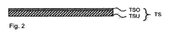
図6は、支持基板のポリマー含有上層TSOの厚さに対する、接合構造体VBS及び配線接続構造体VSSの主要な幾何学的寸法又は構造の高さを示す。接合構造体VBS及び配線接続構造体VSSは第1チップCH1の下側に配置される。配線接続構造体VSSの高さは接合構造体VBSの高さより大きい。主に、接合構造体VBSは、第1チップCH1の下側と支持基板TSの上側との距離を維持する役割を果たす。その場合、接合構造体VBSは、主にポリマー材料からなる支持基板TSの最上層TSOと接触する。接合構造体VBSはほぼ上層TSOの上側に載置されるか、又は場合によっては僅かに上層TSOに突入していてよい。 FIG. 6 shows the height of the main geometrical dimensions or structures of the bonding structure VBS and the wiring connection structure VSS with respect to the thickness of the polymer-containing upper layer TSO of the supporting substrate. The bonding structure VBS and the wiring connection structure VSS are arranged below the first chip CH1. The height of the wiring connection structure VSS is larger than the height of the bonding structure VBS. The joint structure VBS mainly serves to maintain the distance between the lower side of the first chip CH1 and the upper side of the support substrate TS. In that case, the bonding structure VBS comes into contact with the uppermost layer TSO of the support substrate TS mainly made of a polymer material. The bonding structure VBS may be mounted substantially above the upper layer TSO, or may possibly extend slightly into the upper layer TSO.
配線接続構造体VSSはその大きい高さにより支持基板TSのポリマー含有上層TSOを貫通している。後で配線接続構造体VSSの要素と電気的接触を起こす場合、単に支持基板の下層TSUを貫通すればよい。その場合、上層TSOはほぼ維持され、機械的安定性が確保される。 The wiring connection structure VSS penetrates the polymer-containing upper layer TSO of the support substrate TS due to its large height. When making electrical contact with the elements of the wiring connection structure VSS later, it is sufficient to simply penetrate the lower layer TSU of the support substrate. In that case, the upper layer TSO is almost maintained, and mechanical stability is ensured.
図1〜5はそのような部品の主な製造工程を示す:
図1には、支持基板のベース、つまり支持基板の下層TSUが示されている。
Figures 1 to 5 show the main manufacturing steps of such components:
FIG. 1 shows the base of the supporting substrate, that is, the lower layer TSU of the supporting substrate.
その上には、ポリマー含有上層TSOが載置される(図2)。その場合、上層は非常に柔らかいため、配線接続構造体VSSはこれを後ほど容易に貫通できる。特に、上層TSOは液状であってよい。 A polymer-containing upper layer TSO is placed thereon (FIG. 2). In that case, since the upper layer is very soft, the wiring connection structure VSS can easily penetrate it later. In particular, the upper TSO may be liquid.
図3は、その下側に、例えばSAW構造体、BAW構造体、又はダイアフラム等の感受性が高い部品構造体BESを支持する第1チップCH1を示す。部品構造体は、正確な機能を確保するため、揺動自在に第1チップCH1の上側に配置されることを特徴とする。 FIG. 3 shows on the lower side a first chip CH1 which supports a sensitive component structure BES, for example a SAW structure, a BAW structure or a diaphragm. The component structure is characterized in that it is swingably disposed above the first chip CH1 in order to ensure an accurate function.
図4は、例えば部品構造体を外部の回路環境又は部品の更なる回路部品と配線接続するために、配線接続構造体VSSが第1チップCH1の下側に配置される仕方を示す。 FIG. 4 shows how the wiring connection structure VSS is arranged below the first chip CH1, for example for wiring the component structure to an external circuit environment or further circuit components of the component.
図5は、更に第1チップの下側の接合構造体VBSを示す。それにより、部品構造体BESとそのために設けられた支持基板TSとの十分な距離を維持することができるが、接合構造体VBSは、好ましくは、部品構造体BESよりも大きい構造高さを有する。 FIG. 5 further shows the bonding structure VBS on the lower side of the first chip. Thereby, a sufficient distance between the component structure BES and the supporting substrate TS provided for it can be maintained, but the bonding structure VBS preferably has a larger structural height than the component structure BES. .
このように、第1チップCH1におけるその下側のその構造体と支持基板TSとが接合した後、図6に示される部品が得られ、部品構造体は支持基板TSとの十分な距離を有する。接合構造体VBSは自身が閉じられている場合、特に、部品構造体が配置される、遮断された中空空間が得られる。 In this way, after the structure below the first chip CH1 and the supporting substrate TS are joined to each other, the component shown in FIG. 6 is obtained, and the component structure has a sufficient distance from the supporting substrate TS. . If the joining structure VBS is closed, in particular, a closed hollow space is obtained in which the component structures are arranged.
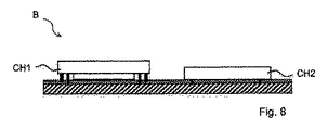
図7は第2チップCH2が配置された支持基板TSの一部を更に示す。第2チップは感受性が高い部品構造体をその表面に備えることを必要としない。そのため、その下側と支持基板TSとが直接接触しても破損しない。第2チップCH2と支持基板TSとの接合構造体は可能であるが、必須ではない。 FIG. 7 further shows a part of the support substrate TS on which the second chip CH2 is arranged. The second chip does not need to have sensitive component structures on its surface. Therefore, even if the lower side and the support substrate TS come into direct contact, they are not damaged. A joint structure between the second chip CH2 and the support substrate TS is possible but not essential.
ここで、図8は、機械的に感受性が高い部品構造体をその下側に有する第1チップCH1とともに感受性が低い第2チップCH2を支持基板上に配置した部品Bを示す。両チップは、支持基板TSのポリマー含有最上層を通る、電気接触構造体をその下側に備える。 Here, FIG. 8 shows a component B in which a second chip CH2 having low sensitivity is arranged on a support substrate together with a first chip CH1 having a component structure having high mechanical sensitivity underneath. Both chips are provided with electrical contact structures underneath, through the polymer-containing top layer of the support substrate TS.
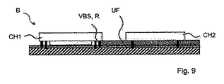
図9は、第2チップCH2が支持基板と直接接触していない実施形態を示す。第2チップCH2と支持基板TSとの間の自由空間が望ましくない場合、第2チップCH2下の容積を、例えばアンダーフィル材UF等の充填材で充填してよい。 FIG. 9 shows an embodiment in which the second chip CH2 is not in direct contact with the support substrate. If the free space between the second chip CH2 and the support substrate TS is not desirable, the volume below the second chip CH2 may be filled with a filler such as an underfill material UF.
第1チップCH1の接合構造体VBSはリング状に閉じられているフレームRとして形成されているので、第1チップCH1の下側の感受性が高い部品構造体にとってもアンダーフィル材UFを塗布することによる危険はない。逆に、充填材UFは第1チップCH1下の中空空間の密閉閉止を向上させることができる。 Since the joining structure VBS of the first chip CH1 is formed as a frame R closed in a ring shape, the underfill material UF is applied to even the highly sensitive component structure below the first chip CH1. There is no danger due to. Conversely, the filler UF can improve the hermetic closure of the hollow space below the first chip CH1.
図10は、配線接続構造体VSSが電気的に接続される場合における、従来の部品に対する本発明の構成の主な利点を示す。有利には、支持基板の上層が硬化される一方で、十分な機械的安定性を与えることができる。なお、信号線を形成して配線構造体の配線接続を行うため、その下の層TSUを貫通し、それにより配線接続構造体VSSを露出させることがただ必要である。このように、例えばレーザを用いて、孔Lを支持基板TSのポリマー層の下に配置された層TSUに作孔してよい。 FIG. 10 shows the main advantages of the configuration of the present invention over conventional components when the wiring connection structure VSS is electrically connected. Advantageously, sufficient mechanical stability can be provided while the upper layer of the support substrate is cured. Note that, in order to form a signal line and perform wiring connection of the wiring structure, it is only necessary to penetrate the layer TSU thereunder, thereby exposing the wiring connection structure VSS. In this way, holes L may be drilled in the layer TSU arranged below the polymer layer of the support substrate TS, for example using a laser.
図11は、通常のリソグラフィ工程によって支持基板の下側に配置され、チップの電気接触部間又はチップの接触部と外部のコンタクトパッドKPを配線接続する、その金属被覆部Mを示す。 FIG. 11 shows a metal covering portion M which is arranged under the supporting substrate by a normal lithography process and interconnects between the electrical contact portions of the chip or the contact portion of the chip and the external contact pad KP.
図12は、信号経路を形成するための金属被覆部Mを下側に設置する前に、個々の孔Lを選択的に配線接続構造体VSSの位置に作孔するのではなく、支持基板TSの下層TSUを完全に除去した実施形態を示す。 FIG. 12 shows that the individual holes L are not selectively formed at the position of the wiring connection structure VSS before the metal coating portion M for forming the signal path is installed on the lower side. 5 shows an embodiment in which the lower TSU is completely removed.
図13及び14は、支持基板と第2チップCH2との間に充填材が配置されていない、支持基板の下側の対応する電気接続を示す。ポリマー層の厚さ及び安定性に応じて、これらはすでに十分な機械的安定性(図14)を自在に有することができる。 FIGS. 13 and 14 show the corresponding electrical connections on the underside of the support substrate, where no filler is arranged between the support substrate and the second chip CH2. Depending on the thickness and the stability of the polymer layers, they can already have sufficient mechanical stability (FIG. 14).
図15は、部品の上側が薄片Fによって被覆される、更なる場合を示す。支持基板上側のチップがどれだけお互いに距離が離れているかに応じて、薄片Fを支持基板の上面と接合するか、又はチップの間で薄片の下の中空空間を取り囲んでよい。薄片が支持基板の上面と接触する場合、例えば支持基板のめっきスルーホールによって、薄片は電位と接続することができる。更に、対応して複数製造された支持基板を個別化してよく、薄片による密閉が個別化によって損なわれない、複数の異なる部品を得る。薄片が支持基板及びチップの側面とともに中空区間を形成する場合、マイクロホンのための後方容積として形成される。 FIG. 15 shows a further case in which the upper side of the part is covered by a slice F. Depending on how far the chips on the support substrate are apart from each other, the flakes F may be joined to the upper surface of the support substrate or may surround the hollow space below the flakes between the chips. When the flake contacts the upper surface of the support substrate, the flake can be connected to an electrical potential, for example, by plated through holes in the support substrate. Furthermore, a corresponding plurality of supporting substrates may be singulated to obtain a plurality of different parts in which the sealing by the slices is not impaired by the singulation. If the slices form a hollow section with the side of the support substrate and the chip, they are formed as a rear volume for the microphone.
図16は、第1チップCH1下の中空空間Hから充填材UFが溢出することを効果的に妨げる、フレームとして形成された接合構造体VBSの保護効果を示す。従って、部品構造体BESは確実に中空空間Hに格納される。 FIG. 16 shows the protective effect of the joint structure VBS formed as a frame, which effectively prevents the filler UF from overflowing from the hollow space H below the first chip CH1. Therefore, the component structure BES is reliably stored in the hollow space H.
第1チップCH1の他にも、更なるチップCH2と第3チップCH3が支持基板の上側に配置されている。 In addition to the first chip CH1, further chips CH2 and third chips CH3 are arranged above the support substrate.
図17は、信号経路SLを支持基板の上面の金属被覆部により形成する場合を示す。その場合、信号経路はチップの接触部から美品の縁に向かって延在し、コンタクトパッドKPで終端してよい。それにより、簡易な方法で、外部の回路環境に差込接続することが可能である。 FIG. 17 shows a case where the signal path SL is formed by a metal coating on the upper surface of the support substrate. In that case, the signal path may extend from the contact portion of the chip toward the edge of the beauty product and terminate at the contact pad KP. Thereby, it is possible to plug-in to an external circuit environment in a simple manner.
折曲線KNは、チップ又は他の回路要素が支持基板の上側で支持基板の屈曲後、折曲縁KNにおいてまだ十分な場所を有するように、選択される。屈曲後、支持基板をその部品とともに上面で、例えばポリマー又は合成樹脂等の成型材により成型することができる。 The folding curve KN is selected such that the chip or other circuit element still has enough space at the folding edge KN after bending of the support substrate above the support substrate. After bending, the support substrate together with its components can be molded on the top side with a molding material, for example a polymer or a synthetic resin.
そのような成型材は図18に示される。その場合、成形材は部品の上側全体を被覆する。 Such a molding is shown in FIG. In that case, the molding material covers the entire upper side of the part.
図19は、マイクロホンとしての部品の実施形態を示す。第1チップCH1は部品構造体としてダイアフラムMBとバックプレートRPとを支持する。支持基板の上側はカバーDにより被覆される。カバーDには孔が音響入力孔として構成される。カバーDは第1チップCH1と並んで後方容積RVを更に含む。それとともに、音響的な短絡が回避され、音響入力と後方容積RVとの間に音響シールADが形成される。この場合、接合構造体は完全には閉止されないため、第1チップCH1のダイアフラムMBの下の容積と後方容積RVとの間のガス交換が可能である。 FIG. 19 shows an embodiment of a component as a microphone. The first chip CH1 supports the diaphragm MB and the back plate RP as a component structure. The upper side of the support substrate is covered with a cover D. A hole is formed in the cover D as a sound input hole. The cover D further includes a rear volume RV alongside the first chip CH1. At the same time, an acoustic short circuit is avoided and an acoustic seal AD is formed between the acoustic input and the rear volume RV. In this case, since the joining structure is not completely closed, gas exchange between the volume below the diaphragm MB of the first tip CH1 and the rear volume RV is possible.
図20は、ダイアフラムの下の後方容積を、支持基板つまりその最上層TSOに凹部により設ける場合を示す。 FIG. 20 shows the case where the rear volume below the diaphragm is provided by a recess in the supporting substrate, that is, the uppermost layer TSO thereof.
支持基板の最上層TSOが厚いほど、後方容積RVは大きい。その場合、配線接続構造体は、最上層TSOを完全に貫通するほど十分に長い。 As the uppermost layer TSO of the support substrate is thicker, the rear volume RV is larger. In that case, the wiring connection structure is long enough to completely penetrate the uppermost layer TSO.
図21は、後方容積の一部が支持基板の凹部AUにより第1チップと並んで形成される、マイクロホンとしての部品の更なる実施形態を示す。支持基板の更なる孔Lは音響入力孔を示す。接合構造体は、音響的短絡を回避するため、この実施形態ではリング状に閉じられている。 FIG. 21 shows a further embodiment of a component as a microphone, in which a part of the rear volume is formed alongside the first chip by a recess AU in the support substrate. Further holes L in the support substrate indicate sound input holes. The joining structure is closed in a ring in this embodiment in order to avoid acoustic short circuits.
部品も部品の製造方法も、例示又は記載された実施形態に限定されない。
以下に本願の出願当初の特許請求の範囲に記載された発明を付記する。
[C1] 電気部品(B)において以下を備える:
少なくとも1つのポリマー層(TSO)を有する支持基板(TS)と、
その下側に接合構造体(VBR)と金属配線接続構造体(VSS)を有する第1チップ(CH1)、
以下を特徴とする、
前記第1チップ(CH1)は前記支持基板(TS)上に配置され、
前記接合構造体(VBS)は前記ポリマー層(TSO)上に載置されるか、又は前記ポリマー層(TSO)内において貫通することなく突出し、
前記配線接続構造体(VSS)は前記ポリマー層(TSO)を貫通する。
[C2] 前記第1チップ(CH1)は、MEMSチップ、NEMSチップ、ICチップ、光電子チップ、アクチュエータチップ、単にパッシブ回路素子を備えるチップの中から選択される、C1に記載の部品。
[C3] 前記支持基板(TS)は、半導体内蔵基板、回路基板、LTCC基板、HTCC基板、有機支持薄片、無機支持薄片、金属薄片、単結晶基板、多結晶基板、半導体基板、セラミック基板、ガラス基板から選択される層(TSU)を更に備える、C1又は2に記載の部品。
[C4] C1〜3の何れか1項に記載の部品において、
前記第1チップ(CH1)と前記支持基板(TS)との間の隙間を更に有し、
感受性が高い構造体(BES)は、前記支持基板(TS)と接触することなく、前記第1チップ(CH1)の下側に配置される。
[C5] 前記隙間は側方において前記チップの下側にフレーム(R)として形成された前記接合構造体(VBS)により画定され、前記チップ(CH1)、前記フレーム(R)、及び前記支持基板(TS)は中空空間(H)を取り囲む、C4項に記載の部品。
[C6] C1〜5の何れか1項に記載の部品において、
主要構成要素としての前記接合構造体(VBS)はポリマー、Cu、Al、Ag、又はAuそして、
主要構成要素としての前記配線接続構造体(VSS)はCu、Al、Ag、又はAuを含有する。
[C7] C1〜6の何れか1項に記載の部品において、前記配線接続構造体(VSS)は、 バンプ接合体若しくは金属ピラー又は
前記チップ(CH1)及び/又は前記支持基板(TS)にめっきスルーホールを有する。
有する。
[C8] 前記接合構造体(VBS)は円形若しくは長方形の断面を有する支持体又は支持フレーム(R)を含む、C1〜7の何れか1項に記載の部品。
[C9] C1〜8の何れか1項に記載の部品は第2チップ(CH2)を更に備え、前記第2チップは
前記第1チップ(CH1)の上方又は上に配置されるか、
前記第1チップ(CH1)と並んで前記支持基板(TS)上に配置される。
[C10] C1〜9の何れか1項に記載の部品は、以下を更に備える:
積層体、型材(VM)、プリント工程による被塗布材、若しくは前記第1チップ(CH1)上方の薄片(F)を有するチューブシート及び/又は、
前記支持基板(TS)の領域上に直接配置され、チップ材と前記支持基板(TS)との間の隙間を充填する充填材(UF)。
[C11] 金属からなるトップ層を前記第1チップ(CH1)上方に更に備える、C1〜10の何れか1項に記載の部品。
[C12] C1〜11の何れか1項に記載の部品において、
前記第1チップ(CH1)又は更なるチップ(CH2、CH3)はセンサチップであって、カバー(D)の下に配置され、
前記センサチップは前記カバー(D)の孔を通して前記部品(B)の周囲と接続される。
[C13] C12に記載の部品において、
前記部品はマイクロホンであって、
前記センサチップは電気音響トランスデューサ構造体を備え、
前記カバー(D)の下には後方容積(RV)が構成される。
[C14] 少なくとも1つの更なるチップ(CH2、CH3)を備える部品において、前記更なるチップ(CH2、CH3)は前記支持基板(TS)の上側に配置され、前記支持基板(TS)上の前記第1チップ(CH1)と前記更なるチップ(CH2、CH3)との間の接続区間は非常に長いため、前記チップ(CH1、CH2、CH3)間の前記支持基板(TS)は湾曲可能である、C1〜13の何れか1項に記載の部品。
[C15] 外部の回路環境との差込接続により接合し配線接続されるために備えられた露出するストリップ導体(SL)を前記支持基板(TS)の上側に更に備える、C1〜14の何れか1項に記載の部品。
[C16] 電気部品(B)の製造方法は以下のステップを備える:
第1チップ(CH1)を設けるステップと、
前記第1チップ(CH1)の下側に金属接合構造体(VBS)と金属配線接続構造体(VSS)を形成するステップにおいて、前記両構造体(VBS、VSS)は異なる高さを有するステップと、
柔らかいポリマー層(TSO)を有する支持基板(TS)を設けるステップと、
前記第1チップ(CH1)と前記支持基板(TS)とを接合するステップにおいて、前記配線接続構造体(VSS)は前記ポリマー層(TSO)を貫通し、前記接合構造体(VBS)は前記ポリマー層(TSO)を貫通することなく前記ポリマー層(TSO)と接触するステップ。
[C17] 前記ポリマー層(TSO)を、前記第1チップ(CH1)を載置した後に、照射又は加熱によって硬化させる、C16に記載の方法。
[C18] C17に記載の方法において、
前記支持基板(TS)は前記ポリマー層(TSO)の下に層を含み、前記層は好適な光波長領域において透明であり、前記ポリマー層(TSO)を前記波長領域において曝射により硬化する。
[C19] 前記第1チップ(CH1)と並んで又は前記第1チップ(CH1)上にまた更なるチップ(CH2)又は複数の更なるチップ(CH2、CH3)を配置する、C16〜18の何れか1項に記載の方法。
[C20] 充填材(UF)はチップ材(CH1、CH2、CH3)と前記支持基板(TS)との間の領域に配置される、C16〜19の何れか1項に記載の方法。
[C21] 型材(VM)及び/又は薄片(F)は前記第1チップ(CH1)の上方に載置される、C16〜20の何れか1項に記載の方法、
[C22] 金属トップ層は前記第1チップ(CH1)の上方に載置される、C16〜21の何れか1項に記載の方法。
[C23] 前記支持基板(TS)は前記ポリマー層(TSO)の下に更なる層(TSU)を含み、前記更なる層(TSU)は、前記ポリマー層(TSO)の硬化後、完全に又は選択的に前記配線接続構造体(VSS)の領域から除去され、前記配線接続構造体(VSS)は露出される、C16〜22の何れか1項に記載の方法。
[C24] 前記配線接続構造体(VSS)の露出はレーザを用いて行われる、C23に記載の方法。
[C25] C23又は24の何れか1項に記載の方法において、
前記配線接続構造体(VSS)は接触部(KP)を備え、
前記接触部(KP)はストリップ導体(SL)の形成により露出された後、前記支持基板(TS)の下側で接触される。
[C26] 前記部品は複数の他の部品とともに複数製造され、前記他の部品から個別化することにより分離される、C16〜25の何れか1項に記載の方法。
[C27] C16〜26の何れか1項に記載の方法において、
前記部品の上側に、Cu、Ni、及び黒ニッケルを含有する層を有する複合層を付着させ、その後、
Ni含有材料を選択的に除去することで、印字される。
[C28] 導電性構造体(SL)は前記チップ(CH1)の表面及び/又は前記支持基板(TS)の表面に金属若しくは合金を被着すること又は金属含有ナノ粒子を噴射することにより形成される、C16〜27の何れか1項に記載の方法。
Neither the parts nor the method of manufacturing the parts are limited to the illustrated or described embodiments.
Hereinafter, the invention described in the claims at the time of filing the application of the present application is additionally described.
[C1] The electrical component (B) comprises:
A support substrate (TS) having at least one polymer layer (TSO);
A first chip (CH1) having a bonding structure (VBR) and a metal wiring connection structure (VSS) thereunder;
Characterized by:
The first chip (CH1) is disposed on the support substrate (TS),
The bonding structure (VBS) rests on the polymer layer (TSO) or projects without penetrating within the polymer layer (TSO);
The wiring connection structure (VSS) penetrates the polymer layer (TSO).
[C2] The component according to C1, wherein the first chip (CH1) is selected from a MEMS chip, a NEMS chip, an IC chip, an optoelectronic chip, an actuator chip, and a chip having only a passive circuit element.
[C3] The support substrate (TS) is a substrate with a built-in semiconductor, a circuit substrate, an LTCC substrate, an HTCC substrate, an organic support flake, an inorganic support flake, a metal flake, a single crystal substrate, a polycrystalline substrate, a semiconductor substrate, a ceramic substrate, and glass The component of C1 or 2, further comprising a layer (TSU) selected from a substrate.
[C4] The component according to any one of C1 to C3,
A gap between the first chip (CH1) and the support substrate (TS);
The sensitive structure (BES) is arranged below the first chip (CH1) without contacting the support substrate (TS).
[C5] The gap is laterally defined by the bonding structure (VBS) formed as a frame (R) below the chip, and includes the chip (CH1), the frame (R), and the support substrate. (TS) The component according to item C4, surrounding the hollow space (H).
[C6] In the component according to any one of C1 to 5,
The bonding structure (VBS) as a main component is a polymer, Cu, Al, Ag, or Au; and
The wiring connection structure (VSS) as a main component contains Cu, Al, Ag, or Au.
[C7] In the component according to any one of C1 to 6, the wiring connection structure (VSS) includes a bump joint, a metal pillar, or
The chip (CH1) and / or the support substrate (TS) have a plated through hole.
Have.
[C8] The component according to any one of C1 to 7, wherein the joining structure (VBS) includes a support or a support frame (R) having a circular or rectangular cross section.
[C9] The component according to any one of C1 to 8 further includes a second chip (CH2), wherein the second chip is
Disposed above or above the first chip (CH1);
It is arranged on the support substrate (TS) along with the first chip (CH1).
[C10] The component according to any one of C1 to 9 further comprises:
A laminate, a mold (VM), a material to be coated by a printing process, or a tube sheet having a thin section (F) above the first chip (CH1) and / or
A filler (UF) that is disposed directly on the region of the support substrate (TS) and fills a gap between the chip material and the support substrate (TS);
[C11] The component according to any one of C1 to 10, further comprising a top layer made of a metal above the first chip (CH1).
[C12] In the component according to any one of C1 to 11,
The first chip (CH1) or the further chips (CH2, CH3) are sensor chips and are arranged under the cover (D);
The sensor chip is connected to the periphery of the component (B) through a hole in the cover (D).
[C13] The component according to C12,
The component is a microphone,
The sensor chip includes an electroacoustic transducer structure,
A rear volume (RV) is formed below the cover (D).
[C14] In a component including at least one further chip (CH2, CH3), the further chip (CH2, CH3) is disposed above the support substrate (TS), and is provided on the support substrate (TS). Since the connection section between the first chip (CH1) and the further chips (CH2, CH3) is very long, the support substrate (TS) between the chips (CH1, CH2, CH3) can be curved. , C1-13.
[C15] Any of C1 to C14 further including an exposed strip conductor (SL) provided on the upper side of the support substrate (TS) for being joined and connected by an insertion connection with an external circuit environment. The component according to item 1.
[C16] The method for producing the electric component (B) includes the following steps:
Providing a first chip (CH1);
Forming a metal bonding structure (VBS) and a metal wiring connection structure (VSS) below the first chip (CH1), wherein the two structures (VBS, VSS) have different heights; ,
Providing a support substrate (TS) having a soft polymer layer (TSO);
In the step of bonding the first chip (CH1) and the support substrate (TS), the wiring connection structure (VSS) penetrates the polymer layer (TSO), and the bonding structure (VBS) includes the polymer Contacting the polymer layer (TSO) without penetrating the layer (TSO).
[C17] The method according to C16, wherein the polymer layer (TSO) is cured by irradiation or heating after placing the first chip (CH1).
[C18] The method according to C17,
The support substrate (TS) includes a layer under the polymer layer (TSO), the layer being transparent in a suitable light wavelength range, and curing the polymer layer (TSO) by irradiation in the wavelength range.
[C19] Any of C16 to C18, further disposing a further chip (CH2) or a plurality of further chips (CH2, CH3) alongside or on the first chip (CH1). Or the method of claim 1.
[C20] The method according to any one of C16 to C19, wherein the filler (UF) is disposed in a region between the chip material (CH1, CH2, CH3) and the support substrate (TS).
[C21] The method according to any one of C16 to C20, wherein the template (VM) and / or the flakes (F) are placed above the first chip (CH1).
[C22] The method according to any one of C16 to C21, wherein a metal top layer is placed above the first chip (CH1).
[C23] The support substrate (TS) includes a further layer (TSU) under the polymer layer (TSO), wherein the further layer (TSU) is completely or completely after curing of the polymer layer (TSO). 23. The method of any of C16-22, wherein the wiring connection structure (VSS) is selectively removed from a region of the wiring connection structure (VSS) and the wiring connection structure (VSS) is exposed.
[C24] The method according to C23, wherein the exposing of the wiring connection structure (VSS) is performed using a laser.
[C25] The method according to any one of C23 or 24,
The wiring connection structure (VSS) includes a contact portion (KP);
After the contact portion (KP) is exposed by forming the strip conductor (SL), it is contacted below the support substrate (TS).
[C26] The method of any of C16-25, wherein the component is manufactured in plurality with a plurality of other components and separated by individualization from the other component.
[C27] The method according to any one of C16 to C26,
Depositing a composite layer having a layer containing Cu, Ni, and black nickel on top of the component,
Printing is performed by selectively removing the Ni-containing material.
[C28] The conductive structure (SL) is formed by applying a metal or an alloy to the surface of the chip (CH1) and / or the surface of the support substrate (TS), or by spraying metal-containing nanoparticles. The method according to any one of C16 to C27.
符号の説明
AU: 凹部
B: 部品
BES: 部品構造体
CH1: 第1チップ
CH2: 第2チップ
CH3: 第3チップ
D: カバー
F: 薄片
H: 中空空間
KN: 折曲線
KP: コンタクトパッド
L: 孔
M: 金属被覆部
MB: ダイアフラム
R: フレーム
RP: バックプレート
RV: 後方容積
SL: 信号経路
TS: 支持基板
TSO: 支持基板最上層
TSU: 支持基板最上層の下の層
UF: 充填材又はアンダーフィル材
VBS: 接合構造体
VM: 成型材
VSS: 配線接続構造体
AU: concave portion B: component BES: component structure CH1: first chip CH2: second chip CH3: third chip D: cover F: flake H: hollow space KN: folding curve KP: contact pad L: hole M: Metal coating part MB: Diaphragm R: Frame RP: Back plate RV: Back volume SL: Signal path TS: Support substrate TSO: Support substrate top layer TSU: Layer under support substrate top layer UF: Filler or underfill Material VBS: Joint structure VM: Molding material VSS: Wiring connection structure
Claims (13)
少なくとも1つのポリマー層(TSO)を有する支持基板(TS)と、
その下側に接合構造体(VBS)と金属配線接続構造体(VSS)を有する第1チップ(CH1)、
以下を特徴とする、
前記第1チップ(CH1)は前記支持基板(TS)上に配置され、
前記接合構造体(VBS)は前記ポリマー層(TSO)上に載置されるか、又は前記ポリマー層(TSO)内において貫通することなく突出し、
前記金属配線接続構造体(VSS)は前記ポリマー層(TSO)を貫通し、
前記第1チップ(CH1)と支持基板(TS)との間の隙間と、ここにおいて、感受性が高い構造体(BES)は、前記支持基板(TS)と接触することなく、前記第1チップ(CH1)の下側に配置され、
前記第1チップ(CH1)と並んで前記支持基板(TS)上に配置され、かつ前記第1チップ(CH1)と電気的に接触する、第2チップ(CH2)、
ここにおいて、前記部品は、外部の回路環境との差込接続により接合し配線接続されるために備えられた露出するストリップ導体(SL)を前記支持基板(TS)の上側に更に備える。 The electrical component (B) comprises:
A support substrate (TS) having at least one polymer layer (TSO);
A first chip (CH1) having a bonding structure (VBS) and a metal wiring connection structure (VSS) thereunder;
Characterized by:
The first chip (CH1) is disposed on the support substrate (TS),
The bonding structure (VBS) rests on the polymer layer (TSO) or projects without penetrating within the polymer layer (TSO);
The metal wiring connection structure (VSS) penetrates the polymer layer (TSO);
The gap between the first chip (CH1) and the support substrate (TS) and the highly sensitive structure (BES) here do not come into contact with the support substrate (TS). CH1).
A second chip (CH2) that is arranged on the support substrate (TS) alongside the first chip (CH1) and is in electrical contact with the first chip (CH1);
Here, the component further includes an exposed strip conductor (SL) provided for joining and wiring connection by plug-in connection with an external circuit environment on the upper side of the support substrate (TS).
主要構成要素としての前記接合構造体(VBS)はポリマー、Cu、Al、Ag、又はAuを含み、そして、
主要構成要素としての前記金属配線接続構造体(VSS)はCu、Al、Ag、又はAuを含む。 The component according to any one of claims 1 to 4,
The bonding structure (VBS) as a main component comprises a polymer, Cu, Al, Ag, or Au; and
The metal wiring connection structure (VSS) as a main component includes Cu, Al, Ag, or Au.
バンプ接合体若しくは金属ピラー又は
前記第1チップ(CH1)及び/又は前記支持基板(TS)にめっきスルーホールを有する。 The component according to any one of claims 1 to 5, wherein the metal wiring connection structure (VSS) comprises:
There is a plated through hole in the bump assembly, the metal pillar, or the first chip (CH1) and / or the support substrate (TS).
積層体、型材(VM)、プリント工程による被塗布材、若しくは前記第1チップ(CH1)上方の薄片(F)を有するチューブシート及び/又は、
前記支持基板(TS)の領域上に直接配置され、チップ材と前記支持基板(TS)との間の隙間を充填する充填材(UF)。 The component according to any one of claims 1 to 7 further comprises:
A laminate, a mold (VM), a material to be coated by a printing process, or a tube sheet having a thin section (F) above the first chip (CH1) and / or
A filler (UF) that is disposed directly on the region of the support substrate (TS) and fills a gap between the chip material and the support substrate (TS);
第1チップ(CH1)を設けるステップと、
前記第1チップ(CH1)の下側に金属接合構造体(VBS)と金属配線接続構造体(VSS)を形成するステップにおいて、前記両構造体(VBS、VSS)は異なる高さを有するステップと、
柔らかいポリマー層(TSO)を有する支持基板(TS)を設けるステップと、
前記第1チップ(CH1)と前記支持基板(TS)とを接合するステップにおいて、前記金属配線接続構造体(VSS)は前記ポリマー層(TSO)を貫通し、前記金属接合構造体(VBS)は前記ポリマー層(TSO)を貫通することなく前記ポリマー層(TSO)と接触するステップと、
ここにおいて、前記第1チップ(CH1)に加えて、更なる第2チップ(CH2)が前記支持基板(TS)上に配置され、
ここにおいて、前記ポリマー層(TSO)が、前記第1チップ(CH1)及び前記第2チップ(CH2)が載置された後に、照射又は加熱によって硬化される、
ここにおいて、前記支持基板(TS)は前記ポリマー層(TSO)の下に更なる層(TSU)を含み、前記更なる層(TSU)は、前記ポリマー層(TSO)の硬化後、完全に又は選択的に前記金属配線接続構造体(VSS)の領域から除去され、前記金属配線接続構造体(VSS)は露出され、
前記金属配線接続構造体(VSS)は接触部(KP)を備え、
前記接触部(KP)は、前記金属配線接続構造体(VSS)が露出された後、ストリップ導体(SL)の形成により、前記支持基板(TS)の下側で接触され、
ここにおいて、充填材(UF)は、前記第2チップ(CH2)と前記支持基板(TS)との間の領域に配置される。 The method for producing an electrical component (B) comprises the following steps:
Providing a first chip (CH1);
Forming a metal bonding structure (VBS) and a metal wiring connection structure (VSS) below the first chip (CH1), wherein the two structures (VBS, VSS) have different heights; ,
Providing a support substrate (TS) having a soft polymer layer (TSO);
In the step of bonding the first chip (CH1) and the support substrate (TS), the metal wiring connection structure (VSS) penetrates the polymer layer (TSO), and the metal bonding structure (VBS) Contacting the polymer layer (TSO) without penetrating the polymer layer (TSO);
Here, in addition to the first chip (CH1), a further second chip (CH2) is arranged on the support substrate (TS),
Here, after the first chip (CH1) and the second chip (CH2) are mounted, the polymer layer (TSO) is cured by irradiation or heating.
Here, said support substrate (TS) comprises a further layer (TSU) under said polymer layer (TSO), said further layer (TSU) being completely or completely after curing of said polymer layer (TSO). Selectively removing from the region of the metal interconnect structure (VSS), exposing the metal interconnect structure (VSS),
The metal wiring connection structure (VSS) includes a contact portion (KP);
After the metal wiring connection structure (VSS) is exposed, the contact portion (KP) is contacted below the support substrate (TS) by forming a strip conductor (SL),
Here, the filler (UF) is disposed in a region between the second chip (CH2) and the support substrate (TS).
前記支持基板(TS)は前記ポリマー層(TSO)の下に層を含み、前記層は光波長領域において透明であり、前記ポリマー層(TSO)を前記波長領域において曝射により硬化する。 The method of claim 10, wherein
The support substrate (TS) includes a layer below the polymer layer (TSO), wherein the layer is transparent in the optical wavelength range, and cures the polymer layer (TSO) by exposure in the wavelength range.
Applications Claiming Priority (3)
| Application Number | Priority Date | Filing Date | Title |
|---|---|---|---|
| DE102014118214.6 | 2014-12-09 | ||
| DE102014118214.6A DE102014118214B4 (en) | 2014-12-09 | 2014-12-09 | Easily manufactured electrical component and method for producing an electrical component |
| PCT/EP2015/074148 WO2016091438A1 (en) | 2014-12-09 | 2015-10-19 | Simple to produce electric component and method for producing an electric component |
Publications (3)
| Publication Number | Publication Date |
|---|---|
| JP2018506171A JP2018506171A (en) | 2018-03-01 |
| JP2018506171A5 JP2018506171A5 (en) | 2018-11-08 |
| JP6672301B2 true JP6672301B2 (en) | 2020-03-25 |
Family
ID=54330770
Family Applications (1)
| Application Number | Title | Priority Date | Filing Date |
|---|---|---|---|
| JP2017530257A Active JP6672301B2 (en) | 2014-12-09 | 2015-10-19 | Electrical parts that can be easily manufactured and method for manufacturing electrical parts |
Country Status (10)
| Country | Link |
|---|---|
| US (1) | US11245977B2 (en) |
| EP (1) | EP3231010B1 (en) |
| JP (1) | JP6672301B2 (en) |
| KR (1) | KR102561741B1 (en) |
| CN (1) | CN107004664B (en) |
| BR (1) | BR112017012118A2 (en) |
| DE (1) | DE102014118214B4 (en) |
| ES (1) | ES2873364T3 (en) |
| MX (1) | MX2017007254A (en) |
| WO (1) | WO2016091438A1 (en) |
Families Citing this family (4)
| Publication number | Priority date | Publication date | Assignee | Title |
|---|---|---|---|---|
| US11067768B2 (en) * | 2017-11-16 | 2021-07-20 | Tdk Taiwan Corp. | Optical member driving mechanism |
| CN111003682A (en) * | 2018-10-08 | 2020-04-14 | 凤凰先驱股份有限公司 | Electronic package and manufacturing method thereof |
| CN111821567A (en) * | 2019-03-30 | 2020-10-27 | 深圳硅基仿生科技有限公司 | Electronic package and implantable device |
| CN111422821A (en) * | 2020-03-13 | 2020-07-17 | 清华大学 | Microsystem packaging method |
Family Cites Families (28)
| Publication number | Priority date | Publication date | Assignee | Title |
|---|---|---|---|---|
| US7434305B2 (en) * | 2000-11-28 | 2008-10-14 | Knowles Electronics, Llc. | Method of manufacturing a microphone |
| DE10164494B9 (en) | 2001-12-28 | 2014-08-21 | Epcos Ag | Encapsulated low-profile device and method of manufacture |
| US6781231B2 (en) | 2002-09-10 | 2004-08-24 | Knowles Electronics Llc | Microelectromechanical system package with environmental and interference shield |
| JP4484544B2 (en) | 2004-02-25 | 2010-06-16 | 京セラ株式会社 | Manufacturing method of high frequency module |
| US7323675B2 (en) * | 2005-09-21 | 2008-01-29 | Sigurd Microelectronics Corp. | Packaging structure of a light-sensing device with a spacer wall |
| DE102005053765B4 (en) | 2005-11-10 | 2016-04-14 | Epcos Ag | MEMS package and method of manufacture |
| JP2008091639A (en) * | 2006-10-02 | 2008-04-17 | Nec Electronics Corp | Electronic equipment, and manufacturing method thereof |
| JP4903540B2 (en) | 2006-11-29 | 2012-03-28 | 京セラ株式会社 | Substrate for encapsulating microelectromechanical components, substrate for encapsulating microelectromechanical components in plural shapes, microelectromechanical device, and manufacturing method of microelectronic mechanical device |
| KR100826394B1 (en) * | 2007-05-17 | 2008-05-02 | 삼성전기주식회사 | Method for manufacturing semiconductor package |
| CN101325823B (en) | 2007-06-11 | 2011-08-17 | 美律实业股份有限公司 | Encapsulation construction for silicon crystal microphone |
| TWI348872B (en) | 2007-10-17 | 2011-09-11 | Ind Tech Res Inst | Electro-acoustic sensing device |
| US8900931B2 (en) * | 2007-12-26 | 2014-12-02 | Skyworks Solutions, Inc. | In-situ cavity integrated circuit package |
| DE102009019446B4 (en) | 2009-04-29 | 2014-11-13 | Epcos Ag | MEMS microphone |
| US8227904B2 (en) | 2009-06-24 | 2012-07-24 | Intel Corporation | Multi-chip package and method of providing die-to-die interconnects in same |
| US8428286B2 (en) | 2009-11-30 | 2013-04-23 | Infineon Technologies Ag | MEMS microphone packaging and MEMS microphone module |
| TWI451538B (en) | 2010-01-19 | 2014-09-01 | Gen Mems Corp | Mems microphone packages and fabrication methods thereof |
| DE102010006132B4 (en) | 2010-01-29 | 2013-05-08 | Epcos Ag | Miniaturized electrical component with a stack of a MEMS and an ASIC |
| EP2420470B1 (en) | 2010-08-18 | 2015-10-14 | Nxp B.V. | MEMS Microphone |
| US9239386B2 (en) * | 2011-10-05 | 2016-01-19 | Infineon Technologies Ag | Sonic sensors and packages |
| US9210516B2 (en) * | 2012-04-23 | 2015-12-08 | Infineon Technologies Ag | Packaged MEMS device and method of calibrating a packaged MEMS device |
| JP5565544B2 (en) * | 2012-08-01 | 2014-08-06 | 株式会社村田製作所 | Electronic components and electronic component modules |
| CN102917303B (en) | 2012-10-30 | 2015-03-18 | 无锡芯奥微传感技术有限公司 | Microphone packaged by plastic casing |
| US9040349B2 (en) * | 2012-11-15 | 2015-05-26 | Amkor Technology, Inc. | Method and system for a semiconductor device package with a die to interposer wafer first bond |
| DE102012112058B4 (en) | 2012-12-11 | 2020-02-27 | Snaptrack, Inc. | MEMS component and method for encapsulating MEMS components |
| CN103491490B (en) | 2013-08-16 | 2019-03-19 | 上海集成电路研发中心有限公司 | A kind of MEMS microphone structure and its manufacturing method |
| CN103888879A (en) | 2014-03-31 | 2014-06-25 | 山东共达电声股份有限公司 | Directional MEMS microphone |
| US9666514B2 (en) * | 2015-04-14 | 2017-05-30 | Invensas Corporation | High performance compliant substrate |
| JP6450416B2 (en) * | 2016-04-29 | 2019-01-09 | キヤノン株式会社 | Ultrasonic transducer and manufacturing method thereof |
-
2014
- 2014-12-09 DE DE102014118214.6A patent/DE102014118214B4/en active Active
-
2015
- 2015-10-19 MX MX2017007254A patent/MX2017007254A/en unknown
- 2015-10-19 KR KR1020177013197A patent/KR102561741B1/en active IP Right Grant
- 2015-10-19 US US15/532,454 patent/US11245977B2/en active Active
- 2015-10-19 EP EP15781664.6A patent/EP3231010B1/en active Active
- 2015-10-19 JP JP2017530257A patent/JP6672301B2/en active Active
- 2015-10-19 WO PCT/EP2015/074148 patent/WO2016091438A1/en active Application Filing
- 2015-10-19 ES ES15781664T patent/ES2873364T3/en active Active
- 2015-10-19 BR BR112017012118-2A patent/BR112017012118A2/en not_active Application Discontinuation
- 2015-10-19 CN CN201580063060.0A patent/CN107004664B/en active Active
Also Published As
| Publication number | Publication date |
|---|---|
| WO2016091438A1 (en) | 2016-06-16 |
| DE102014118214A1 (en) | 2016-06-09 |
| EP3231010A1 (en) | 2017-10-18 |
| KR20170094143A (en) | 2017-08-17 |
| EP3231010B1 (en) | 2021-03-03 |
| US11245977B2 (en) | 2022-02-08 |
| ES2873364T3 (en) | 2021-11-03 |
| US20170272855A1 (en) | 2017-09-21 |
| JP2018506171A (en) | 2018-03-01 |
| MX2017007254A (en) | 2017-10-16 |
| KR102561741B1 (en) | 2023-07-28 |
| BR112017012118A2 (en) | 2018-01-02 |
| DE102014118214B4 (en) | 2024-02-22 |
| CN107004664B (en) | 2021-02-05 |
| CN107004664A (en) | 2017-08-01 |
Similar Documents
| Publication | Publication Date | Title |
|---|---|---|
| JP5220004B2 (en) | Flip-chip device and manufacturing method thereof | |
| US7843021B2 (en) | Double-side mountable MEMS package | |
| JP5193898B2 (en) | Semiconductor device and electronic device | |
| US8520396B2 (en) | Method for producing an electronic module | |
| CN102659069B (en) | Part and its manufacture method with least one MEMS component | |
| JP5894186B2 (en) | Packaged electronic devices | |
| JP6672301B2 (en) | Electrical parts that can be easily manufactured and method for manufacturing electrical parts | |
| TWI469233B (en) | Packaging system with hollow package | |
| CN104422553A (en) | Micromechanical sensor device and corresponding manufacturing method | |
| US11492250B2 (en) | Electronic device and method for manufacturing an electronic device | |
| JP2013105784A (en) | Optical sensor device and method for manufacturing the same | |
| JP2007174622A (en) | Acoustic sensor | |
| CN101252092A (en) | Multi-chip packaging structure and making method thereof | |
| JP2018506171A5 (en) | ||
| JP5708688B2 (en) | Manufacturing method of sensor package | |
| JP2010245157A (en) | Component for wiring and method of manufacturing the same, and electronic device package used by incorporating the component for wiring and method of manufacturing the same | |
| CN209497431U (en) | A kind of wafer level packaging structure of filter | |
| CN103208467A (en) | Package module with embedded package and method for manufacturing the same | |
| US9253886B2 (en) | Module and production method | |
| JP2019201121A (en) | Premold substrate and manufacturing method thereof, and hollow semiconductor device and manufacturing method thereof | |
| KR101708531B1 (en) | Cap bump structure for reliable wlb(wafer level bonding) and method of manufacture | |
| TW201208026A (en) | MEMS carrier and fabrication method thereof | |
| JP5429890B2 (en) | WIRING ELECTRONIC COMPONENT AND ITS MANUFACTURING METHOD, AND ELECTRONIC DEVICE PACKAGE USING THE WIRING ELECTRONIC COMPONENT AND ITS MANUFACTURING METHOD | |
| JP4695672B2 (en) | Semiconductor device | |
| JP2010186770A (en) | Sensor device |
Legal Events
| Date | Code | Title | Description |
|---|---|---|---|
| A521 | Request for written amendment filed |
Free format text: JAPANESE INTERMEDIATE CODE: A523 Effective date: 20180925 |
|
| A621 | Written request for application examination |
Free format text: JAPANESE INTERMEDIATE CODE: A621 Effective date: 20180925 |
|
| A977 | Report on retrieval |
Free format text: JAPANESE INTERMEDIATE CODE: A971007 Effective date: 20190809 |
|
| A131 | Notification of reasons for refusal |
Free format text: JAPANESE INTERMEDIATE CODE: A131 Effective date: 20190820 |
|
| A521 | Request for written amendment filed |
Free format text: JAPANESE INTERMEDIATE CODE: A523 Effective date: 20191007 |
|
| A131 | Notification of reasons for refusal |
Free format text: JAPANESE INTERMEDIATE CODE: A131 Effective date: 20191023 |
|
| A521 | Request for written amendment filed |
Free format text: JAPANESE INTERMEDIATE CODE: A523 Effective date: 20200123 |
|
| TRDD | Decision of grant or rejection written | ||
| A01 | Written decision to grant a patent or to grant a registration (utility model) |
Free format text: JAPANESE INTERMEDIATE CODE: A01 Effective date: 20200204 |
|
| A61 | First payment of annual fees (during grant procedure) |
Free format text: JAPANESE INTERMEDIATE CODE: A61 Effective date: 20200304 |
|
| R150 | Certificate of patent or registration of utility model |
Ref document number: 6672301 Country of ref document: JP Free format text: JAPANESE INTERMEDIATE CODE: R150 |
|
| R250 | Receipt of annual fees |
Free format text: JAPANESE INTERMEDIATE CODE: R250 |
|
| R250 | Receipt of annual fees |
Free format text: JAPANESE INTERMEDIATE CODE: R250 |