JP6643799B2 - センサ、及び、これを用いた情報取得装置 - Google Patents
センサ、及び、これを用いた情報取得装置 Download PDFInfo
- Publication number
- JP6643799B2 JP6643799B2 JP2014242519A JP2014242519A JP6643799B2 JP 6643799 B2 JP6643799 B2 JP 6643799B2 JP 2014242519 A JP2014242519 A JP 2014242519A JP 2014242519 A JP2014242519 A JP 2014242519A JP 6643799 B2 JP6643799 B2 JP 6643799B2
- Authority
- JP
- Japan
- Prior art keywords
- terahertz wave
- polarization
- polarization direction
- unit
- antenna
- Prior art date
- Legal status (The legal status is an assumption and is not a legal conclusion. Google has not performed a legal analysis and makes no representation as to the accuracy of the status listed.)
- Active
Links
- 230000010287 polarization Effects 0.000 claims description 170
- 239000004020 conductor Substances 0.000 claims description 80
- 238000001514 detection method Methods 0.000 claims description 53
- 230000003287 optical effect Effects 0.000 claims description 47
- 239000000758 substrate Substances 0.000 claims description 37
- 238000006243 chemical reaction Methods 0.000 claims description 35
- 230000005540 biological transmission Effects 0.000 claims description 17
- 230000005484 gravity Effects 0.000 claims description 11
- 239000013078 crystal Substances 0.000 claims description 9
- 230000004888 barrier function Effects 0.000 claims description 7
- 239000004065 semiconductor Substances 0.000 description 38
- 229910000530 Gallium indium arsenide Inorganic materials 0.000 description 15
- 230000008859 change Effects 0.000 description 14
- 239000000463 material Substances 0.000 description 14
- 238000010586 diagram Methods 0.000 description 13
- 239000000523 sample Substances 0.000 description 12
- 230000005684 electric field Effects 0.000 description 7
- 238000000034 method Methods 0.000 description 7
- JBRZTFJDHDCESZ-UHFFFAOYSA-N AsGa Chemical compound [As]#[Ga] JBRZTFJDHDCESZ-UHFFFAOYSA-N 0.000 description 6
- 229910001218 Gallium arsenide Inorganic materials 0.000 description 6
- 229910052751 metal Inorganic materials 0.000 description 6
- 239000002184 metal Substances 0.000 description 6
- 230000004048 modification Effects 0.000 description 6
- 238000012986 modification Methods 0.000 description 6
- 239000000126 substance Substances 0.000 description 6
- 238000007689 inspection Methods 0.000 description 4
- 229910000673 Indium arsenide Inorganic materials 0.000 description 3
- VYPSYNLAJGMNEJ-UHFFFAOYSA-N Silicium dioxide Chemical compound O=[Si]=O VYPSYNLAJGMNEJ-UHFFFAOYSA-N 0.000 description 3
- 230000001419 dependent effect Effects 0.000 description 3
- 238000005530 etching Methods 0.000 description 3
- 230000006870 function Effects 0.000 description 3
- RPQDHPTXJYYUPQ-UHFFFAOYSA-N indium arsenide Chemical compound [In]#[As] RPQDHPTXJYYUPQ-UHFFFAOYSA-N 0.000 description 3
- 238000005259 measurement Methods 0.000 description 3
- 229910005540 GaP Inorganic materials 0.000 description 2
- 229910000661 Mercury cadmium telluride Inorganic materials 0.000 description 2
- 229910000577 Silicon-germanium Inorganic materials 0.000 description 2
- UMIVXZPTRXBADB-UHFFFAOYSA-N benzocyclobutene Chemical compound C1=CC=C2CCC2=C1 UMIVXZPTRXBADB-UHFFFAOYSA-N 0.000 description 2
- 239000000919 ceramic Substances 0.000 description 2
- 230000008878 coupling Effects 0.000 description 2
- 238000010168 coupling process Methods 0.000 description 2
- 238000005859 coupling reaction Methods 0.000 description 2
- 238000001312 dry etching Methods 0.000 description 2
- 238000010894 electron beam technology Methods 0.000 description 2
- 238000003384 imaging method Methods 0.000 description 2
- 238000009616 inductively coupled plasma Methods 0.000 description 2
- 239000012071 phase Substances 0.000 description 2
- -1 polyethylene terephthalate Polymers 0.000 description 2
- 230000008569 process Effects 0.000 description 2
- 239000010453 quartz Substances 0.000 description 2
- 239000011347 resin Substances 0.000 description 2
- 229920005989 resin Polymers 0.000 description 2
- 238000003860 storage Methods 0.000 description 2
- 210000000689 upper leg Anatomy 0.000 description 2
- 229910017115 AlSb Inorganic materials 0.000 description 1
- 229910000980 Aluminium gallium arsenide Inorganic materials 0.000 description 1
- 229910004613 CdTe Inorganic materials 0.000 description 1
- 229910005543 GaSe Inorganic materials 0.000 description 1
- 241000238631 Hexapoda Species 0.000 description 1
- 229910012463 LiTaO3 Inorganic materials 0.000 description 1
- 206010028980 Neoplasm Diseases 0.000 description 1
- 239000004698 Polyethylene Substances 0.000 description 1
- 229910052581 Si3N4 Inorganic materials 0.000 description 1
- XUIMIQQOPSSXEZ-UHFFFAOYSA-N Silicon Chemical compound [Si] XUIMIQQOPSSXEZ-UHFFFAOYSA-N 0.000 description 1
- 239000004809 Teflon Substances 0.000 description 1
- 229920006362 Teflon® Polymers 0.000 description 1
- 229910007709 ZnTe Inorganic materials 0.000 description 1
- 229910052782 aluminium Inorganic materials 0.000 description 1
- XAGFODPZIPBFFR-UHFFFAOYSA-N aluminium Chemical compound [Al] XAGFODPZIPBFFR-UHFFFAOYSA-N 0.000 description 1
- 229910021417 amorphous silicon Inorganic materials 0.000 description 1
- 201000011510 cancer Diseases 0.000 description 1
- 239000003990 capacitor Substances 0.000 description 1
- 239000000969 carrier Substances 0.000 description 1
- 238000004891 communication Methods 0.000 description 1
- 150000001875 compounds Chemical class 0.000 description 1
- 230000007423 decrease Effects 0.000 description 1
- 230000003247 decreasing effect Effects 0.000 description 1
- 230000001066 destructive effect Effects 0.000 description 1
- 239000003989 dielectric material Substances 0.000 description 1
- CSJLBAMHHLJAAS-UHFFFAOYSA-N diethylaminosulfur trifluoride Substances CCN(CC)S(F)(F)F CSJLBAMHHLJAAS-UHFFFAOYSA-N 0.000 description 1
- 230000000694 effects Effects 0.000 description 1
- 230000005611 electricity Effects 0.000 description 1
- 238000005868 electrolysis reaction Methods 0.000 description 1
- 230000005670 electromagnetic radiation Effects 0.000 description 1
- 238000000605 extraction Methods 0.000 description 1
- 239000012467 final product Substances 0.000 description 1
- HZXMRANICFIONG-UHFFFAOYSA-N gallium phosphide Chemical compound [Ga]#P HZXMRANICFIONG-UHFFFAOYSA-N 0.000 description 1
- 239000011521 glass Substances 0.000 description 1
- 239000012535 impurity Substances 0.000 description 1
- 238000002347 injection Methods 0.000 description 1
- 239000007924 injection Substances 0.000 description 1
- 239000012212 insulator Substances 0.000 description 1
- 238000001459 lithography Methods 0.000 description 1
- 238000004519 manufacturing process Methods 0.000 description 1
- 238000001451 molecular beam epitaxy Methods 0.000 description 1
- ORQBXQOJMQIAOY-UHFFFAOYSA-N nobelium Chemical compound [No] ORQBXQOJMQIAOY-UHFFFAOYSA-N 0.000 description 1
- 230000010355 oscillation Effects 0.000 description 1
- 230000003071 parasitic effect Effects 0.000 description 1
- 239000008188 pellet Substances 0.000 description 1
- 230000035699 permeability Effects 0.000 description 1
- 238000000206 photolithography Methods 0.000 description 1
- 230000000704 physical effect Effects 0.000 description 1
- 239000004033 plastic Substances 0.000 description 1
- 229920003023 plastic Polymers 0.000 description 1
- 229920000573 polyethylene Polymers 0.000 description 1
- 229920000139 polyethylene terephthalate Polymers 0.000 description 1
- 239000005020 polyethylene terephthalate Substances 0.000 description 1
- 239000000843 powder Substances 0.000 description 1
- 239000000047 product Substances 0.000 description 1
- 238000012827 research and development Methods 0.000 description 1
- 229910052710 silicon Inorganic materials 0.000 description 1
- 239000010703 silicon Substances 0.000 description 1
- HQVNEWCFYHHQES-UHFFFAOYSA-N silicon nitride Chemical compound N12[Si]34N5[Si]62N3[Si]51N64 HQVNEWCFYHHQES-UHFFFAOYSA-N 0.000 description 1
- 229910052814 silicon oxide Inorganic materials 0.000 description 1
- 125000006850 spacer group Chemical group 0.000 description 1
- 238000004528 spin coating Methods 0.000 description 1
- 239000002887 superconductor Substances 0.000 description 1
- 230000007704 transition Effects 0.000 description 1
- 230000005641 tunneling Effects 0.000 description 1
- 238000000927 vapour-phase epitaxy Methods 0.000 description 1
- 125000000391 vinyl group Chemical group [H]C([*])=C([H])[H] 0.000 description 1
- 229920002554 vinyl polymer Polymers 0.000 description 1
- 239000013585 weight reducing agent Substances 0.000 description 1
Images


Classifications
-
- G—PHYSICS
- G01—MEASURING; TESTING
- G01J—MEASUREMENT OF INTENSITY, VELOCITY, SPECTRAL CONTENT, POLARISATION, PHASE OR PULSE CHARACTERISTICS OF INFRARED, VISIBLE OR ULTRAVIOLET LIGHT; COLORIMETRY; RADIATION PYROMETRY
- G01J5/00—Radiation pyrometry, e.g. infrared or optical thermometry
- G01J5/59—Radiation pyrometry, e.g. infrared or optical thermometry using polarisation; Details thereof
-
- A—HUMAN NECESSITIES
- A61—MEDICAL OR VETERINARY SCIENCE; HYGIENE
- A61B—DIAGNOSIS; SURGERY; IDENTIFICATION
- A61B5/00—Measuring for diagnostic purposes; Identification of persons
- A61B5/05—Detecting, measuring or recording for diagnosis by means of electric currents or magnetic fields; Measuring using microwaves or radio waves
- A61B5/0507—Detecting, measuring or recording for diagnosis by means of electric currents or magnetic fields; Measuring using microwaves or radio waves using microwaves or terahertz waves
-
- A—HUMAN NECESSITIES
- A61—MEDICAL OR VETERINARY SCIENCE; HYGIENE
- A61B—DIAGNOSIS; SURGERY; IDENTIFICATION
- A61B5/00—Measuring for diagnostic purposes; Identification of persons
- A61B5/68—Arrangements of detecting, measuring or recording means, e.g. sensors, in relation to patient
- A61B5/6801—Arrangements of detecting, measuring or recording means, e.g. sensors, in relation to patient specially adapted to be attached to or worn on the body surface
- A61B5/6813—Specially adapted to be attached to a specific body part
- A61B5/6828—Leg
-
- G—PHYSICS
- G01—MEASURING; TESTING
- G01J—MEASUREMENT OF INTENSITY, VELOCITY, SPECTRAL CONTENT, POLARISATION, PHASE OR PULSE CHARACTERISTICS OF INFRARED, VISIBLE OR ULTRAVIOLET LIGHT; COLORIMETRY; RADIATION PYROMETRY
- G01J5/00—Radiation pyrometry, e.g. infrared or optical thermometry
- G01J5/02—Constructional details
- G01J5/08—Optical arrangements
- G01J5/0837—Microantennas, e.g. bow-tie
-
- G—PHYSICS
- G01—MEASURING; TESTING
- G01N—INVESTIGATING OR ANALYSING MATERIALS BY DETERMINING THEIR CHEMICAL OR PHYSICAL PROPERTIES
- G01N21/00—Investigating or analysing materials by the use of optical means, i.e. using sub-millimetre waves, infrared, visible or ultraviolet light
- G01N21/17—Systems in which incident light is modified in accordance with the properties of the material investigated
- G01N21/21—Polarisation-affecting properties
-
- G—PHYSICS
- G01—MEASURING; TESTING
- G01N—INVESTIGATING OR ANALYSING MATERIALS BY DETERMINING THEIR CHEMICAL OR PHYSICAL PROPERTIES
- G01N21/00—Investigating or analysing materials by the use of optical means, i.e. using sub-millimetre waves, infrared, visible or ultraviolet light
- G01N21/17—Systems in which incident light is modified in accordance with the properties of the material investigated
- G01N21/25—Colour; Spectral properties, i.e. comparison of effect of material on the light at two or more different wavelengths or wavelength bands
- G01N21/31—Investigating relative effect of material at wavelengths characteristic of specific elements or molecules, e.g. atomic absorption spectrometry
- G01N21/35—Investigating relative effect of material at wavelengths characteristic of specific elements or molecules, e.g. atomic absorption spectrometry using infrared light
- G01N21/3581—Investigating relative effect of material at wavelengths characteristic of specific elements or molecules, e.g. atomic absorption spectrometry using infrared light using far infrared light; using Terahertz radiation
-
- G—PHYSICS
- G01—MEASURING; TESTING
- G01N—INVESTIGATING OR ANALYSING MATERIALS BY DETERMINING THEIR CHEMICAL OR PHYSICAL PROPERTIES
- G01N21/00—Investigating or analysing materials by the use of optical means, i.e. using sub-millimetre waves, infrared, visible or ultraviolet light
- G01N21/84—Systems specially adapted for particular applications
- G01N21/88—Investigating the presence of flaws or contamination
- G01N21/94—Investigating contamination, e.g. dust
Description
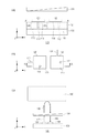
本実施形態に係るセンサ100がテラヘルツ波を発生及び検出する様子について、図1(c)を用いて説明する。図1(c)はセンサ100によるテラヘルツ波の発生及び検出を説明する図である。テラヘルツ波の周波数は、30GHz以上30THz以下である。
上述の実施形態のセンサ100の構成について、より具体的に説明する。センサ100は、周波数fTHz=0.45THzのテラヘルツ波の発信及び受信を行うセンサである。
・GaAs基板上に形成したGaAs/AlGaAs/及びGaAs/AlAs、InGaAs/GaAs/AlAs
・InP基板上に形成したInGaAs/AlGaAsSb
・InAs基板上に形成したInAs/AlAsSb及びInAs/AlSb
・Si基板上に形成したSiGe/SiGe
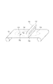
本実施例のセンサ800について図7を参照して説明する。図7は、センサ800の構成を説明する図である。実施例1の偏波変換部310は、発信部の第一のアンテナと結合する第一の偏波107の偏波方向を変更する第一の変換部と、テラヘルツ波の偏波方向を変更して受信部の第二のアンテナと結合する第二の偏波108に変換する第二の変換部とを有していた。すなわち、第一の変換部と第二の変換部とを用いて第一の偏波107を第二の偏波108に変換していた。それに対し、本実施例のセンサ800は、発信部から発信された第一の偏波107の偏波方向を変更することにより得られたテラヘルツ波を受信部で受信する。なお、上述のセンサ100と同様の構成には同じ符号を付し、詳細な説明は省略する。
本実施例では、被検体602の情報を取得する情報取得装置600(以下、「装置600」と呼ぶ)について説明する。図5は、装置600の構成を説明する図である。図5では、被検体602として人の大腿を用い、被検体602の情報として被検体602の画像を取得する場合を例として示した。
センサ100を用いた情報取得装置710(以下、「装置710」と呼ぶ)について、図6を参照して説明する。図6は、装置710を説明する図である。装置710は、被検体730に線状にテラヘルツ波709を照射して、被検体730で反射したテラヘルツ波709を検出するラインセンサ700と、情報取得部755(以下、「取得部755」と呼ぶ)とを有する。
Claims (18)
- テラヘルツ波の発信及び受信を行うセンサであって、
基板と、
テラヘルツ波を発生する発生素子、及び前記発生素子が発生した第一の偏波方向のテラヘルツ波を放射する第一のアンテナ、を有する発信部と、
前記第一のアンテナから放射されたテラヘルツ波の偏波方向を変更する偏波変換部と、前記第一の偏波方向と異なる第二の偏波方向のテラヘルツ波を受信する第二のアンテナ、及び前記第二のアンテナが受信したテラヘルツ波を検出する検出素子と、を有する受信部と、を有し、
前記発信部と前記受信部とは、前記基板上に配置されており、
前記第一のアンテナは、第一の導体と、第二の導体と、前記第一の導体と前記第二の導体との間に配置されている第一の誘電体と、を有し、
前記第二のアンテナは、第三の導体と、第四の導体と、前記第三の導体と前記第四の導体との間に配置されている前記第二の誘電体と、を有し、
前記発生素子は、前記第一の導体と前記第二の導体との間で且つ前記第一の導体の重心からシフトした位置に配置されており、
前記検出素子は、前記第三の導体と前記第四の導体との間で且つ前記第三の導体の重心からシフトした位置に配置されており、
前記発生素子と前記第一の導体の重心とを結ぶ直線と、前記検出素子と前記第三の導体の重心とを結ぶ直線とは、交差する
ことを特徴とするセンサ。 - 前記偏波変換部は、前記発生素子が発生したテラヘルツ波の偏波方向を前記第一の偏波方向から第三の偏波方向に変更する第一の変換部と、前記第三の偏波方向を前記第二の偏波方向に変更する第二の変換部と、を有する
ことを特徴とする請求項1に記載のセンサ。 - 前記第一の変換部と前記第二の変換部とは、一体である
ことを特徴とする請求項2に記載のセンサ。 - 前記第一の変換部は、テラヘルツ波が前記発信部から発信されてから被検体に到達するまでの伝搬経路上に配置されており、
前記第二の変換部は、テラヘルツ波が前記被検体で反射してから前記受信部に入射するまでの伝搬経路上に配置されている
ことを特徴とする請求項2又は3に記載のセンサ。 - 前記偏波変換部は、テラヘルツ波が前記発信部から発信されてから被検体に到達するまでの伝搬経路上、又は、テラヘルツ波が前記被検体で反射してから前記受信部に入射するまでの伝搬経路上に配置されている
ことを特徴とする請求項1乃至3のいずれか一項に記載のセンサ。 - 前記第一の偏波方向のテラヘルツ波及び前記第二の偏波方向のテラヘルツ波は、直線偏波であり、前記第一の偏波方向と前記第二の偏波方向とは交差する
ことを特徴とする請求項1乃至5のいずれか一項に記載のセンサ。 - 前記第一の偏波方向と前記第二の偏波方向とは、直交する
ことを特徴とする請求項6に記載のセンサ。 - 前記偏波変換部は、1/4波長板を含み、
前記1/4波長板は、結晶軸が前記第一の偏波方向のテラヘルツ波の光軸及び前記第二の偏波方向のテラヘルツ波の光軸に対して回転する方向になるように配置されている
ことを特徴とする請求項1乃至7のいずれか一項に記載のセンサ。 - 前記1/4波長板は、fast軸及びslow軸と前記第一の偏波方向及び前記第二の偏波方向とがなす角が45度となるように配置されている
ことを特徴とする請求項8に記載のセンサ。 - 複数の前記受信部を有し、
隣り合う前記受信部同士の距離、又は、隣り合う前記発信部と前記受信部との距離は、前記第一の偏波方向のテラヘルツ波及び前記第二の偏波方向のテラヘルツ波の波長の2倍以下であることを特徴とする請求項1乃至9のいずれか一項に記載のセンサ。 - 前記偏波変換部は、前記発信部及び前記受信部の上に集積されている
ことを特徴とする請求項1乃至10のいずれか一項に記載のセンサ。 - 前記第一の誘電体と、前記第二の誘電体とは同一の誘電体であることを特徴とする請求項1乃至11のいずれか一項に記載のセンサ。
- 前記発信部は、前記基板の上に配置されており、
前記受信部は、前記発信部の上に配置されている
ことを特徴とする請求項1乃至11のいずれか一項に記載のセンサ。 - 前記受信部は、前記基板の上に配置されており、
前記発信部は、前記受信部の上に配置されている
ことを特徴とする請求項1乃至11のいずれか一項に記載のセンサ。 - 前記発生素子は負性抵抗素子を含む
ことを特徴とする請求項1乃至14のいずれか一項に記載のセンサ。 - 前記検出素子は、整流素子を含む
ことを特徴とする請求項1乃至15のいずれか一項に記載のセンサ。 - 前記整流素子は、ショットキーバリアダイオードである
ことを特徴とする請求項16に記載のセンサ。 - 請求項1乃至17のいずれか一項に記載のセンサと、
前記センサの検出結果を用いて被検体の情報を取得する情報取得部と、を有することを特徴とする情報取得装置。
Priority Applications (2)
| Application Number | Priority Date | Filing Date | Title |
|---|---|---|---|
| JP2014242519A JP6643799B2 (ja) | 2014-11-28 | 2014-11-28 | センサ、及び、これを用いた情報取得装置 |
| US14/948,108 US9958330B2 (en) | 2014-11-28 | 2015-11-20 | Sensor and information acquisition apparatus using sensor |
Applications Claiming Priority (1)
| Application Number | Priority Date | Filing Date | Title |
|---|---|---|---|
| JP2014242519A JP6643799B2 (ja) | 2014-11-28 | 2014-11-28 | センサ、及び、これを用いた情報取得装置 |
Publications (3)
| Publication Number | Publication Date |
|---|---|
| JP2016102770A JP2016102770A (ja) | 2016-06-02 |
| JP2016102770A5 JP2016102770A5 (ja) | 2017-12-28 |
| JP6643799B2 true JP6643799B2 (ja) | 2020-02-12 |
Family
ID=56088058
Family Applications (1)
| Application Number | Title | Priority Date | Filing Date |
|---|---|---|---|
| JP2014242519A Active JP6643799B2 (ja) | 2014-11-28 | 2014-11-28 | センサ、及び、これを用いた情報取得装置 |
Country Status (2)
| Country | Link |
|---|---|
| US (1) | US9958330B2 (ja) |
| JP (1) | JP6643799B2 (ja) |
Families Citing this family (10)
| Publication number | Priority date | Publication date | Assignee | Title |
|---|---|---|---|---|
| US8571614B1 (en) | 2009-10-12 | 2013-10-29 | Hypres, Inc. | Low-power biasing networks for superconducting integrated circuits |
| US10222416B1 (en) | 2015-04-14 | 2019-03-05 | Hypres, Inc. | System and method for array diagnostics in superconducting integrated circuit |
| JP2017075923A (ja) * | 2015-10-16 | 2017-04-20 | パイオニア株式会社 | 計測装置 |
| US10804850B2 (en) * | 2017-08-26 | 2020-10-13 | Innovative Micro Technology | Gas sensor using mm wave cavity |
| DE102018125050A1 (de) * | 2018-10-10 | 2020-04-16 | Osram Opto Semiconductors Gmbh | Optoelektronischer Sensor |
| CN109449545B (zh) * | 2018-12-19 | 2024-02-13 | 桂林电子科技大学 | 一种可实现吸波模式和极化转换模式切换的太赫兹变换器 |
| JP7286389B2 (ja) * | 2019-04-15 | 2023-06-05 | キヤノン株式会社 | 無線通信装置、無線通信システムおよび通信方法 |
| JP7413672B2 (ja) * | 2019-07-25 | 2024-01-16 | 日本電気株式会社 | アンテナ装置、無線送信機、無線受信機、及び無線通信システム |
| US11879722B2 (en) * | 2020-02-27 | 2024-01-23 | Iida Co., Ltd. | Method and system for estimating convergence of changes in dimensions of molded article over time |
| CN114070907B (zh) * | 2020-07-30 | 2024-03-26 | 荣耀终端有限公司 | 镜头装饰组件及电子设备 |
Family Cites Families (21)
| Publication number | Priority date | Publication date | Assignee | Title |
|---|---|---|---|---|
| US4339660A (en) * | 1980-05-15 | 1982-07-13 | Erwin Sick Gmbh Optik-Elektronik | Reflection light barrier apparatus for recognizing both strongly and weakly reflecting objects |
| US5227800A (en) * | 1988-04-19 | 1993-07-13 | Millitech Corporation | Contraband detection system |
| JPH0887755A (ja) * | 1994-09-13 | 1996-04-02 | Sony Corp | 光学装置 |
| JP2000278039A (ja) * | 1999-03-19 | 2000-10-06 | Hitachi Cable Ltd | 偏波共用アンテナ |
| GB2359716B (en) * | 2000-02-28 | 2002-06-12 | Toshiba Res Europ Ltd | An imaging apparatus and method |
| WO2004008196A1 (ja) * | 2002-07-13 | 2004-01-22 | Autocloning Technology Ltd. | 偏光解析装置 |
| JP2004177198A (ja) | 2002-11-26 | 2004-06-24 | Hitachi Ltd | 電磁波画像処理装置 |
| KR100787988B1 (ko) * | 2003-06-25 | 2007-12-24 | 캐논 가부시끼가이샤 | 고주파 전기 신호 제어 장치 및 센싱 시스템 |
| JP4012125B2 (ja) * | 2003-06-25 | 2007-11-21 | キヤノン株式会社 | 電磁波制御装置およびセンシングシステム |
| US7123185B2 (en) * | 2004-04-14 | 2006-10-17 | Safeview, Inc. | Enhanced surveilled subject imaging |
| JP2006145513A (ja) | 2004-11-17 | 2006-06-08 | Semiconductor Res Found | ダイオード発振素子を用いたイメージングシステムおよびイメージング方法 |
| JP4235251B2 (ja) * | 2006-11-10 | 2009-03-11 | パナソニック株式会社 | 偏波切換・指向性可変アンテナ |
| JP4662070B2 (ja) * | 2006-11-30 | 2011-03-30 | 日本無線株式会社 | 2周波複直交偏波導波管スロットアレーアンテナおよび複直交偏波通信システム |
| JP5125858B2 (ja) * | 2008-08-01 | 2013-01-23 | ソニー株式会社 | 光学遅延装置 |
| KR20130001969A (ko) * | 2011-06-28 | 2013-01-07 | 한국전자통신연구원 | 테라헤르츠파를 이용한 샘플의 분석 방법 및 장치 |
| EP2618128A1 (en) * | 2012-01-19 | 2013-07-24 | Canon Kabushiki Kaisha | Detecting device, detector, and imaging apparatus using the same |
| US9244163B2 (en) * | 2012-05-17 | 2016-01-26 | Farrokh Mohamadi | Integrated ultra wideband, wafer scale, RHCP-LHCP arrays |
| WO2014133098A1 (ja) * | 2013-02-28 | 2014-09-04 | シナノケンシ株式会社 | 情報読取素子およびそれを用いた情報読取装置 |
| US9234797B1 (en) * | 2013-03-05 | 2016-01-12 | Exelis, Inc. | Compact THz imaging detector with an integrated micro-spectrometer spectral tuning matrix |
| JP6214201B2 (ja) * | 2013-05-02 | 2017-10-18 | キヤノン株式会社 | 画像取得装置 |
| US9307159B2 (en) * | 2014-03-04 | 2016-04-05 | Panasonic Intellectual Property Management Co., Ltd. | Polarization image processing apparatus |
-
2014
- 2014-11-28 JP JP2014242519A patent/JP6643799B2/ja active Active
-
2015
- 2015-11-20 US US14/948,108 patent/US9958330B2/en active Active
Also Published As
| Publication number | Publication date |
|---|---|
| US20160169746A1 (en) | 2016-06-16 |
| JP2016102770A (ja) | 2016-06-02 |
| US9958330B2 (en) | 2018-05-01 |
Similar Documents
| Publication | Publication Date | Title |
|---|---|---|
| JP6643799B2 (ja) | センサ、及び、これを用いた情報取得装置 | |
| US9391428B2 (en) | Waveguide element | |
| US7884767B2 (en) | Antenna device | |
| US9236833B2 (en) | Electromagnetic wave generation device and detection device | |
| JP6296681B2 (ja) | 発振素子、発振器及びこれを用いた撮像装置 | |
| US10594260B2 (en) | Element that oscillates or detects terahertz waves | |
| Liu et al. | A multichannel THz detector using integrated bow-tie antennas | |
| Ito et al. | Photonic terahertz-wave generation using slot-antenna-integrated uni-traveling-carrier photodiodes | |
| US20150303559A1 (en) | Oscillation device, reception device and sample information acquisition apparatus | |
| US8957379B2 (en) | Suspended wideband planar skirt antenna having low thermal mass for detection of terahertz radiation | |
| US9437646B2 (en) | Detecting device, detector, and imaging apparatus using the same | |
| US11081604B2 (en) | Device and method for bowtie photoconductive antenna for terahertz wave detection | |
| Clochiatti et al. | Broadband THz detection using InP triple-barrier resonant tunneling diode with integrated antenna | |
| Ito et al. | Broadband photonic terahertz-wave emitter integrating uni-traveling-carrier photodiode and self-complementary planar antenna | |
| JP2011135007A (ja) | 発振素子 | |
| US9052234B2 (en) | Dipole antenna with reflectors having low thermal mass for detection of Terahertz radiation | |
| Ito et al. | Polarisation‐sensitive sub‐terahertz‐wave detector implementing antenna‐integrated zero‐bias Schottky barrier diode | |
| Prost et al. | Triple barrier resonant tunneling diodes for THz emission and sensing | |
| Ito et al. | Polarization-sensitive broadband sub-terahertz-wave detector implementing planar-antenna-integrated schottky barrier diode | |
| Beruete | Quasioptical devices based on extraordinary transmission at THz | |
| Di Gaspare et al. | Sub-terahertz mixer based on heterostructure field effect transistor with integrated antennas | |
| Ito et al. | Broadband and low-noise terahertz-wave detection by InP/InGaAs Fermi-level managed barrier diode | |
| Liu et al. | Research Article A Multichannel THz Detector Using Integrated Bow-Tie Antennas | |
| Park et al. | Portable terahertz scanner for imaging and spectroscopy using InP-related devices | |
| Di Gaspare et al. | Antenna-coupled heterostructure field effect transistors for integrated terahertz heterodyne mixers |
Legal Events
| Date | Code | Title | Description |
|---|---|---|---|
| A521 | Written amendment |
Free format text: JAPANESE INTERMEDIATE CODE: A523 Effective date: 20171115 |
|
| A621 | Written request for application examination |
Free format text: JAPANESE INTERMEDIATE CODE: A621 Effective date: 20171115 |
|
| A131 | Notification of reasons for refusal |
Free format text: JAPANESE INTERMEDIATE CODE: A131 Effective date: 20180724 |
|
| A521 | Written amendment |
Free format text: JAPANESE INTERMEDIATE CODE: A523 Effective date: 20180920 |
|
| A131 | Notification of reasons for refusal |
Free format text: JAPANESE INTERMEDIATE CODE: A131 Effective date: 20190312 |
|
| A521 | Written amendment |
Free format text: JAPANESE INTERMEDIATE CODE: A523 Effective date: 20190511 |
|
| A131 | Notification of reasons for refusal |
Free format text: JAPANESE INTERMEDIATE CODE: A131 Effective date: 20190730 |
|
| A521 | Written amendment |
Free format text: JAPANESE INTERMEDIATE CODE: A523 Effective date: 20190807 |
|
| TRDD | Decision of grant or rejection written | ||
| A01 | Written decision to grant a patent or to grant a registration (utility model) |
Free format text: JAPANESE INTERMEDIATE CODE: A01 Effective date: 20191210 |
|
| A61 | First payment of annual fees (during grant procedure) |
Free format text: JAPANESE INTERMEDIATE CODE: A61 Effective date: 20200107 |
|
| R151 | Written notification of patent or utility model registration |
Ref document number: 6643799 Country of ref document: JP Free format text: JAPANESE INTERMEDIATE CODE: R151 |