JP6631431B2 - 電力変換装置 - Google Patents
電力変換装置 Download PDFInfo
- Publication number
- JP6631431B2 JP6631431B2 JP2016143338A JP2016143338A JP6631431B2 JP 6631431 B2 JP6631431 B2 JP 6631431B2 JP 2016143338 A JP2016143338 A JP 2016143338A JP 2016143338 A JP2016143338 A JP 2016143338A JP 6631431 B2 JP6631431 B2 JP 6631431B2
- Authority
- JP
- Japan
- Prior art keywords
- cooling plate
- semiconductor module
- power converter
- stacking direction
- converter according
- Prior art date
- Legal status (The legal status is an assumption and is not a legal conclusion. Google has not performed a legal analysis and makes no representation as to the accuracy of the status listed.)
- Active
Links
- 238000001816 cooling Methods 0.000 claims description 100
- 239000003990 capacitor Substances 0.000 claims description 44
- 239000004065 semiconductor Substances 0.000 claims description 43
- 239000003507 refrigerant Substances 0.000 claims description 33
- 238000006243 chemical reaction Methods 0.000 claims description 24
- 229910052751 metal Inorganic materials 0.000 claims description 3
- 239000002184 metal Substances 0.000 claims description 3
- 238000007599 discharging Methods 0.000 claims description 2
- 238000003475 lamination Methods 0.000 claims description 2
- 239000000470 constituent Substances 0.000 claims 1
- 230000000694 effects Effects 0.000 description 9
- 239000002826 coolant Substances 0.000 description 6
- 238000010030 laminating Methods 0.000 description 6
- 238000010586 diagram Methods 0.000 description 2
- 229910000838 Al alloy Inorganic materials 0.000 description 1
- 230000005540 biological transmission Effects 0.000 description 1
- 230000005669 field effect Effects 0.000 description 1
- 238000009499 grossing Methods 0.000 description 1
- 230000017525 heat dissipation Effects 0.000 description 1
Images


Classifications
-
- H—ELECTRICITY
- H01—ELECTRIC ELEMENTS
- H01L—SEMICONDUCTOR DEVICES NOT COVERED BY CLASS H10
- H01L23/00—Details of semiconductor or other solid state devices
- H01L23/34—Arrangements for cooling, heating, ventilating or temperature compensation ; Temperature sensing arrangements
- H01L23/42—Fillings or auxiliary members in containers or encapsulations selected or arranged to facilitate heating or cooling
-
- H—ELECTRICITY
- H01—ELECTRIC ELEMENTS
- H01L—SEMICONDUCTOR DEVICES NOT COVERED BY CLASS H10
- H01L25/00—Assemblies consisting of a plurality of individual semiconductor or other solid state devices ; Multistep manufacturing processes thereof
- H01L25/03—Assemblies consisting of a plurality of individual semiconductor or other solid state devices ; Multistep manufacturing processes thereof all the devices being of a type provided for in the same subgroup of groups H01L27/00 - H01L33/00, or in a single subclass of H10K, H10N, e.g. assemblies of rectifier diodes
- H01L25/04—Assemblies consisting of a plurality of individual semiconductor or other solid state devices ; Multistep manufacturing processes thereof all the devices being of a type provided for in the same subgroup of groups H01L27/00 - H01L33/00, or in a single subclass of H10K, H10N, e.g. assemblies of rectifier diodes the devices not having separate containers
- H01L25/07—Assemblies consisting of a plurality of individual semiconductor or other solid state devices ; Multistep manufacturing processes thereof all the devices being of a type provided for in the same subgroup of groups H01L27/00 - H01L33/00, or in a single subclass of H10K, H10N, e.g. assemblies of rectifier diodes the devices not having separate containers the devices being of a type provided for in group H01L29/00
- H01L25/074—Stacked arrangements of non-apertured devices
-
- H—ELECTRICITY
- H01—ELECTRIC ELEMENTS
- H01L—SEMICONDUCTOR DEVICES NOT COVERED BY CLASS H10
- H01L23/00—Details of semiconductor or other solid state devices
- H01L23/28—Encapsulations, e.g. encapsulating layers, coatings, e.g. for protection
-
- H—ELECTRICITY
- H01—ELECTRIC ELEMENTS
- H01L—SEMICONDUCTOR DEVICES NOT COVERED BY CLASS H10
- H01L23/00—Details of semiconductor or other solid state devices
- H01L23/34—Arrangements for cooling, heating, ventilating or temperature compensation ; Temperature sensing arrangements
- H01L23/36—Selection of materials, or shaping, to facilitate cooling or heating, e.g. heatsinks
- H01L23/367—Cooling facilitated by shape of device
- H01L23/3675—Cooling facilitated by shape of device characterised by the shape of the housing
-
- H—ELECTRICITY
- H01—ELECTRIC ELEMENTS
- H01L—SEMICONDUCTOR DEVICES NOT COVERED BY CLASS H10
- H01L23/00—Details of semiconductor or other solid state devices
- H01L23/34—Arrangements for cooling, heating, ventilating or temperature compensation ; Temperature sensing arrangements
- H01L23/40—Mountings or securing means for detachable cooling or heating arrangements ; fixed by friction, plugs or springs
- H01L23/4006—Mountings or securing means for detachable cooling or heating arrangements ; fixed by friction, plugs or springs with bolts or screws
- H01L23/4012—Mountings or securing means for detachable cooling or heating arrangements ; fixed by friction, plugs or springs with bolts or screws for stacked arrangements of a plurality of semiconductor devices
-
- H—ELECTRICITY
- H01—ELECTRIC ELEMENTS
- H01L—SEMICONDUCTOR DEVICES NOT COVERED BY CLASS H10
- H01L23/00—Details of semiconductor or other solid state devices
- H01L23/34—Arrangements for cooling, heating, ventilating or temperature compensation ; Temperature sensing arrangements
- H01L23/46—Arrangements for cooling, heating, ventilating or temperature compensation ; Temperature sensing arrangements involving the transfer of heat by flowing fluids
- H01L23/473—Arrangements for cooling, heating, ventilating or temperature compensation ; Temperature sensing arrangements involving the transfer of heat by flowing fluids by flowing liquids
-
- H—ELECTRICITY
- H01—ELECTRIC ELEMENTS
- H01L—SEMICONDUCTOR DEVICES NOT COVERED BY CLASS H10
- H01L23/00—Details of semiconductor or other solid state devices
- H01L23/48—Arrangements for conducting electric current to or from the solid state body in operation, e.g. leads, terminal arrangements ; Selection of materials therefor
- H01L23/488—Arrangements for conducting electric current to or from the solid state body in operation, e.g. leads, terminal arrangements ; Selection of materials therefor consisting of soldered or bonded constructions
-
- H—ELECTRICITY
- H01—ELECTRIC ELEMENTS
- H01L—SEMICONDUCTOR DEVICES NOT COVERED BY CLASS H10
- H01L25/00—Assemblies consisting of a plurality of individual semiconductor or other solid state devices ; Multistep manufacturing processes thereof
- H01L25/03—Assemblies consisting of a plurality of individual semiconductor or other solid state devices ; Multistep manufacturing processes thereof all the devices being of a type provided for in the same subgroup of groups H01L27/00 - H01L33/00, or in a single subclass of H10K, H10N, e.g. assemblies of rectifier diodes
- H01L25/04—Assemblies consisting of a plurality of individual semiconductor or other solid state devices ; Multistep manufacturing processes thereof all the devices being of a type provided for in the same subgroup of groups H01L27/00 - H01L33/00, or in a single subclass of H10K, H10N, e.g. assemblies of rectifier diodes the devices not having separate containers
- H01L25/07—Assemblies consisting of a plurality of individual semiconductor or other solid state devices ; Multistep manufacturing processes thereof all the devices being of a type provided for in the same subgroup of groups H01L27/00 - H01L33/00, or in a single subclass of H10K, H10N, e.g. assemblies of rectifier diodes the devices not having separate containers the devices being of a type provided for in group H01L29/00
- H01L25/072—Assemblies consisting of a plurality of individual semiconductor or other solid state devices ; Multistep manufacturing processes thereof all the devices being of a type provided for in the same subgroup of groups H01L27/00 - H01L33/00, or in a single subclass of H10K, H10N, e.g. assemblies of rectifier diodes the devices not having separate containers the devices being of a type provided for in group H01L29/00 the devices being arranged next to each other
Description
上記半導体モジュールに電気的に接続された構成部品(31、32、33、34)と、
複数の冷却プレート(40)を備えた積層冷却器(4)と、を有し、
上記複数の冷却プレートと上記半導体モジュールとが少なくとも積層されて、積層体(10)を構成しており、
上記積層体を構成する上記複数の冷却プレートのうちの少なくとも一つは、積層方向(X)への投影面積が、他の上記冷却プレートよりも大きい大面積冷却プレート(41)であり、
上記構成部品の少なくとも一つは、上記積層方向から見たとき上記大面積冷却プレートと重なり、かつ、上記積層方向と直交する一つの方向から見たとき上記積層体と重なる特定位置に配置された、特定配置部品(30)であり、
上記特定配置部品は、上記大面積冷却プレートに、空間を介して対向配置されている、電力変換装置(1)にある。
すなわち、構成部品の少なくとも一つは、積層体の一部ではない特定配置部品であるため、当該構成部品を積層体の一部とした場合に比べ、積層体の積層方向の寸法を小さくすることができる。その結果、積層体の耐振性を向上させることができる。
また、特定配置部品は、上記特定位置に配されているため、大面積冷却プレートによって、直接または間接的に冷却することが可能となる。そのため、構成部品の少なくとも一つを、積層体の一部に組み込むことなく冷却することができる。
なお、特許請求の範囲及び課題を解決する手段に記載した括弧内の符号は、後述する実施形態に記載の具体的手段との対応関係を示すものであり、本発明の技術的範囲を限定するものではない。
電力変換装置の実施形態につき、図1〜図4を参照して説明する。
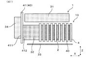
本実施形態の電力変換装置1は、図1、図2に示すごとく、半導体モジュール2と、半導体モジュール2に電気的に接続された構成部品であるコンデンサ31、リアクトル32、及び回路基板33と、積層冷却器4と、を有する。
積層冷却器4は、複数の冷却プレート40を備えている。
複数の冷却プレート40と半導体モジュール2とが少なくとも積層されて、積層体10を構成している。
積層体10を構成する複数の冷却プレート40のうちの少なくとも一つは、積層方向Xへの投影面積が、他の冷却プレート40よりも大きい大面積冷却プレート41である。
また、図1、図3に示すごとく、積層体10は、高さ方向Zにおいて、2つの構成部品の間に配置されている。そして、2つの構成部品のうちの一方であるコンデンサ31が、特定配置部品30となっている。また、高さ方向Zにおいて、積層体10を挟んで互いに反対側に配された2つの構成部品のうちの他方は、半導体モジュール2の信号端子が接続される回路基板33である。すなわち、積層体10は、高さ方向Zにおいて、コンデンサ31と回路基板33との間に配されている。
図1、図2に示すごとく、大面積冷却プレート41は、積層冷却器4のうち、積層方向Xの一端に配されている。そして、大面積冷却プレート41には、積層冷却器4へ冷媒を導入する冷媒導入管421と、積層冷却器4から冷媒を排出する冷媒排出管422とが設けられている。
リアクトル32は、大面積冷却プレート41とこれに隣り合う冷却プレート40との間に配置している。
また、積層冷却器4を構成する部材は、アルミニウム合金等の金属からなる。
インバータ回路部13は、上アームスイッチング素子2uと下アームスイッチング素子2dとを直列接続してなるレッグを、3相分備えている。各スイッチング素子は、IGBT、すなわち絶縁ゲートバイポーラトランジスタからなる。また、上アームスイッチング素子2u及び下アームスイッチング素子2dには、それぞれフライホイールダイオードが逆並列接続されている。各レッグにおける上アームスイッチング素子2uと下アームスイッチング素子2dとの接続点が、それぞれ回転電機52の3つの電極に接続される。なお、スイッチング素子としては、IGBTに限らず、例えば、MOSFET、すなわちMOS型電界効果トランジスタを用いることもできる。
上記電力変換装置1において、構成部品の一つであるコンデンサ31は、特定配置部品30である。そのため、積層体10の積層方向Xの体格を抑制することができると共に、大面積冷却プレート41によるコンデンサ31の冷却が可能となる。
このように、コンデンサ31を上記特定位置に配置することにより、耐振性とコンデンサ31の冷却性確保との両立を図ることができる。
本形態は、図6に示すごとく、特定配置部品30であるコンデンサ31が、大面積冷却プレート41に面接触している形態である。
すなわち、大面積冷却プレート41に、積層方向Xの一方から、コンデンサ31が面接触している。ここで、コンデンサ31と大面積冷却プレート41とは、直接面接触していてもよいし、放熱シート等の伝熱部材を介して面接触していてもよい。
なお、本形態以降において用いた符号のうち、既出の実施形態において用いた符号と同一のものは、特に示さない限り、既出の実施形態におけるものと同様の構成要素等を表す。
その他、実施形態1と同様の作用効果を有する。
本実施形態は、図7に示すごとく、大面積冷却プレート41における積層方向Xの両面に、それぞれ少なくとも一つの構成部品が対向配置されている実施形態である。
すなわち、本実施形態においては、DC−DCコンバータ34を、大面積冷却プレート41における、半導体モジュール2側と反対側の面である第1面411に配置している。また、大面積冷却プレート41における第1面411と反対側の面である第2面412に、リアクトル32が配置されている。さらに、大面積冷却プレート41の第2面412には、特定配置部品30であるコンデンサ31も対向配置されている。
また、図7においては、冷媒導入管421及び冷媒排出管422を省略したが、これらは、積層冷却器4における適切な位置に適宜配設することができる。
その他の構成は、実施形態1と同様である。
その他、実施形態1と同様の作用効果を有する。
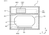
本実施形態は、図8、図9に示すごとく、ケース6を介して、特定配置部品30の熱を、大面積冷却プレート41に放熱できるよう構成された、電力変換装置1の実施形態である。
すなわち、電力変換装置1は、半導体モジュール2とコンデンサ31と積層冷却器4とを収容する金属製のケース6を備えている。大面積冷却プレート41は、ケース6に接触している。そして、特定配置部品30であるコンデンサ31は、ケース6に組み付けられている。
その他の構成は、実施形態2と同様である。
その他、実施形態2と同様の作用効果を有する。
本実施形態においては、図10〜図12に示すごとく、半導体モジュール2が、互いに並列接続された複数の上アームスイッチング素子2uと、互いに並列接続された複数の下アームスイッチング素子2dとを一体化してなる。
本実施形態においては、並列接続された2つの上アームスイッチング素子2uと、並列接続された2つの下アームスイッチング素子2dとの4つのスイッチング素子を、一体化して一つの半導体モジュール2に内蔵している。
その他の構成は、実施形態1と同様である。
その他、実施形態1と同様の作用効果を有する。
本実施形態は、図13に示すごとく、2つの構成部品を特定配置部品30とした実施形態である。
すなわち、特定配置部品30として、コンデンサ31と回路基板33とが、特定位置に配されている。つまり、本実施形態においては、回路基板33も、積層方向Xから見たとき大面積冷却プレート41と重なり、かつ、高さ方向Zから見たとき積層体10と重なる位置に、配されている。
その他の構成は、実施形態1と同様である。
その他、実施形態1と同様の作用効果を有する。
本実施形態は、図14、図15に示すごとく、大面積冷却プレート41以外の冷却プレート40に、冷媒導入管421及び冷媒排出管422が接続されている、電力変換装置1の実施形態である。
本実施形態においては、大面積冷却プレート41には、冷媒導入管421及び冷媒排出管422が接続されていない。そして、積層冷却器4における、大面積冷却プレート41が配された側と反対側の積層方向Xの一端の冷却プレート40に、冷媒導入管421及び冷媒排出管422が接続されている。
その他の構成は、実施形態1と同様である。
その他、実施形態1と同様の作用効果を有する。
本実施形態は、図16に示すごとく、積層体10を、冷却プレート40と半導体モジュール2とによって構成した実施形態である。
すなわち、積層体10に、リアクトル32等の構成部品を積層していない。そして、コンデンサ31を、特定位置に配置した特定配置部品30としている。ここで、コンデンサ31は、積層方向Xから見たとき、その一部分のみが大面積冷却プレート41と重なっている。また、コンデンサ31は、高さ方向Zから見たとき、その一部分のみが積層体10と重なっている。
その他の構成は、実施形態1と同様である。
本実施形態においても、実施形態1と同様の作用効果を奏することができる。
本実施形態は、図17に示すごとく、積層冷却器4における積層方向Xの両端以外の冷却プレート40を、大面積冷却プレート41とした実施形態である。
その他の構成は、実施形態7と同様である。
本実施形態においても、実施形態1と同様の作用効果を奏することができる。
10 積層体
2 半導体モジュール
30 特定配置部品
31 コンデンサ(構成部品)
32 リアクトル(構成部品)
33 回路基板(構成部品)
4 積層冷却器
40 冷却プレート
41 大面積冷却プレート
Claims (11)
- スイッチング素子(2u、2d)を内蔵した半導体モジュール(2)と、
上記半導体モジュールに電気的に接続された構成部品(31、32、33、34)と、
複数の冷却プレート(40)を備えた積層冷却器(4)と、を有し、
上記複数の冷却プレートと上記半導体モジュールとが少なくとも積層されて、積層体(10)を構成しており、
上記積層体を構成する上記複数の冷却プレートのうちの少なくとも一つは、積層方向(X)への投影面積が、他の上記冷却プレートよりも大きい大面積冷却プレート(41)であり、
上記構成部品の少なくとも一つは、上記積層方向から見たとき上記大面積冷却プレートと重なり、かつ、上記積層方向と直交する一つの方向から見たとき上記積層体と重なる特定位置に配置された、特定配置部品(30)であり、
上記特定配置部品は、上記大面積冷却プレートに、空間を介して対向配置されている、電力変換装置(1)。 - 上記積層体は、上記特定配置部品以外の上記構成部品の少なくとも一つを、上記冷却プレート及び上記半導体モジュールと共に積層してなる、請求項1に記載の電力変換装置。
- 上記積層体は、上記積層方向に直交する方向において、2つの上記構成部品の間に配置され、該2つの構成部品のうちの少なくとも一方は、上記特定配置部品である、請求項1又は2に記載の電力変換装置。
- 上記積層方向に直交する方向において、上記積層体を挟んで互いに反対側に配された2つの上記構成部品のうちの一方は、上記半導体モジュールの信号端子が接続される回路基板(33)である、請求項3に記載の電力変換装置。
- 上記特定配置部品は、コンデンサ(31)である、請求項1〜4のいずれか一項に記載の電力変換装置。
- 上記大面積冷却プレートは、上記積層冷却器のうち、上記積層方向の一端に配されている、請求項1〜5のいずれか一項に記載の電力変換装置。
- 上記大面積冷却プレートには、上記積層冷却器へ冷媒を導入する冷媒導入管(421)と、上記積層冷却器から冷媒を排出する冷媒排出管(422)とが設けられている、請求項6に記載の電力変換装置。
- 上記大面積冷却プレートは、上記半導体モジュールと上記構成部品と上記積層冷却器とを収容する金属製のケース(6)に接触しており、上記特定配置部品は、上記ケースに組み付けられている、請求項1〜7のいずれか一項に記載の電力変換装置。
- 上記大面積冷却プレートにおける上記積層方向の両面に、それぞれ少なくとも一つの上記構成部品が対向配置されている、請求項1〜8のいずれか一項に記載の電力変換装置。
- 上記半導体モジュールは、互いに並列接続された複数の上アームスイッチング素子(2u)と、互いに並列接続された複数の下アームスイッチング素子(2d)とを一体化してなる、請求項1〜9のいずれか一項に記載の電力変換装置。
- 上記大面積冷却プレートは、上記積層方向から見たとき、上記半導体モジュールと重なる部分にも、上記特定配置部品と重なる部分にも、内部に冷媒を流通させる冷媒流路(401)を形成してなる、請求項1〜10のいずれか一項に記載の電力変換装置。
Priority Applications (4)
| Application Number | Priority Date | Filing Date | Title |
|---|---|---|---|
| JP2016143338A JP6631431B2 (ja) | 2016-07-21 | 2016-07-21 | 電力変換装置 |
| DE102017116390.5A DE102017116390A1 (de) | 2016-07-21 | 2017-07-20 | Leistungsumwandlervorrichtung mit einem Halbleitermodul mit laminiertem Aufbau |
| US15/654,858 US10410953B2 (en) | 2016-07-21 | 2017-07-20 | Power conversion device including semiconductor module provided with laminated structure |
| CN201710601324.4A CN107645232B (zh) | 2016-07-21 | 2017-07-21 | 包括具有层叠结构的半导体模块的功率转换设备 |
Applications Claiming Priority (1)
| Application Number | Priority Date | Filing Date | Title |
|---|---|---|---|
| JP2016143338A JP6631431B2 (ja) | 2016-07-21 | 2016-07-21 | 電力変換装置 |
Related Child Applications (1)
| Application Number | Title | Priority Date | Filing Date |
|---|---|---|---|
| JP2019152511A Division JP6769533B2 (ja) | 2019-08-23 | 2019-08-23 | 電力変換装置 |
Publications (2)
| Publication Number | Publication Date |
|---|---|
| JP2018014834A JP2018014834A (ja) | 2018-01-25 |
| JP6631431B2 true JP6631431B2 (ja) | 2020-01-15 |
Family
ID=60990115
Family Applications (1)
| Application Number | Title | Priority Date | Filing Date |
|---|---|---|---|
| JP2016143338A Active JP6631431B2 (ja) | 2016-07-21 | 2016-07-21 | 電力変換装置 |
Country Status (4)
| Country | Link |
|---|---|
| US (1) | US10410953B2 (ja) |
| JP (1) | JP6631431B2 (ja) |
| CN (1) | CN107645232B (ja) |
| DE (1) | DE102017116390A1 (ja) |
Families Citing this family (12)
| Publication number | Priority date | Publication date | Assignee | Title |
|---|---|---|---|---|
| WO2018212346A1 (ja) * | 2017-05-18 | 2018-11-22 | パイオニア株式会社 | 制御装置、走査システム、制御方法、およびプログラム |
| WO2019150662A1 (ja) | 2018-01-31 | 2019-08-08 | 日本電気株式会社 | 処理装置、処理方法及びプログラム |
| JP6954176B2 (ja) * | 2018-02-21 | 2021-10-27 | トヨタ自動車株式会社 | ユニット |
| KR102020317B1 (ko) * | 2018-03-30 | 2019-09-10 | 엘에스산전 주식회사 | 가압장치 및 스위칭모듈에서의 스위치 교체 방법 |
| KR102013774B1 (ko) * | 2018-03-30 | 2019-08-23 | 엘에스산전 주식회사 | 무효전력보상장치의 스위치어셈블리 |
| KR102094223B1 (ko) * | 2018-03-30 | 2020-03-27 | 엘에스산전 주식회사 | 무효전력보상장치의 스위치어셈블리 |
| KR102011307B1 (ko) * | 2018-03-30 | 2019-10-21 | 엘에스산전 주식회사 | 무효전력보상장치의 스위치어셈블리 |
| JP6725586B2 (ja) * | 2018-05-18 | 2020-07-22 | 本田技研工業株式会社 | 電力変換装置 |
| CN109560067A (zh) * | 2018-10-14 | 2019-04-02 | 深圳市慧成功率电子有限公司 | 一种分边连接功率电极组合及功率模块 |
| KR102603213B1 (ko) * | 2019-09-02 | 2023-11-16 | 현대자동차주식회사 | 전력 반도체용 냉각 장치 및 그 제조 방법 |
| DE102021203869A1 (de) | 2021-04-19 | 2022-10-20 | Zf Friedrichshafen Ag | Kühlanordnung für Leistungshalbleiter eines Inverters, sowie Elektronikmodul |
| DE102021209724A1 (de) * | 2021-09-03 | 2023-03-09 | Zf Friedrichshafen Ag | Inverteranordnung für ein Fahrzeug sowie Fahrzeug mit der Inverteranordnung |
Family Cites Families (9)
| Publication number | Priority date | Publication date | Assignee | Title |
|---|---|---|---|---|
| JP4506848B2 (ja) * | 2008-02-08 | 2010-07-21 | 株式会社デンソー | 半導体モジュール |
| JP2009232564A (ja) * | 2008-03-21 | 2009-10-08 | Denso Corp | 電力変換装置 |
| JP5326334B2 (ja) * | 2008-04-16 | 2013-10-30 | 株式会社デンソー | パワーコントロールユニット |
| JP5267412B2 (ja) | 2009-10-07 | 2013-08-21 | 株式会社デンソー | 冷媒冷却型両面冷却半導体装置 |
| JP2011165988A (ja) * | 2010-02-11 | 2011-08-25 | Denso Corp | 半導体装置 |
| JP5949616B2 (ja) | 2013-03-22 | 2016-07-13 | トヨタ自動車株式会社 | 積層型冷却器 |
| JP2015136223A (ja) * | 2014-01-16 | 2015-07-27 | トヨタ自動車株式会社 | 電力変換器 |
| JP6156283B2 (ja) | 2014-08-07 | 2017-07-05 | 株式会社デンソー | 電力変換装置 |
| JP6497213B2 (ja) * | 2015-05-26 | 2019-04-10 | 株式会社デンソー | 電力変換装置 |
-
2016
- 2016-07-21 JP JP2016143338A patent/JP6631431B2/ja active Active
-
2017
- 2017-07-20 DE DE102017116390.5A patent/DE102017116390A1/de active Pending
- 2017-07-20 US US15/654,858 patent/US10410953B2/en active Active
- 2017-07-21 CN CN201710601324.4A patent/CN107645232B/zh active Active
Also Published As
| Publication number | Publication date |
|---|---|
| CN107645232B (zh) | 2020-09-22 |
| US10410953B2 (en) | 2019-09-10 |
| CN107645232A (zh) | 2018-01-30 |
| US20180025961A1 (en) | 2018-01-25 |
| DE102017116390A1 (de) | 2018-02-08 |
| JP2018014834A (ja) | 2018-01-25 |
Similar Documents
| Publication | Publication Date | Title |
|---|---|---|
| JP6631431B2 (ja) | 電力変換装置 | |
| JP6540496B2 (ja) | 電力変換装置 | |
| JP5855899B2 (ja) | Dc−dcコンバータ及び電力変換装置 | |
| JP5738794B2 (ja) | 電力変換装置 | |
| US8755185B2 (en) | Semiconductor module | |
| JP5504219B2 (ja) | 電力変換装置 | |
| JP6072492B2 (ja) | コンデンサモジュール及び電力変換装置 | |
| JP5846854B2 (ja) | 一体型電力変換装置及びそれに用いられるdcdcコンバータ装置 | |
| JP5407275B2 (ja) | 電力変換装置 | |
| JP6429721B2 (ja) | 電力変換装置及び鉄道車両 | |
| MX2008012609A (es) | Dispositivo de conversion de energia y su metodo de fabricacion. | |
| JP6136760B2 (ja) | 電力変換装置 | |
| JP2014138445A (ja) | 電力変換装置 | |
| JP6055868B2 (ja) | 電力変換装置 | |
| JP6690478B2 (ja) | 電力変換装置 | |
| JP6977743B2 (ja) | 電力変換装置 | |
| JP6962347B2 (ja) | 電力変換装置 | |
| JP6115430B2 (ja) | 電力変換装置 | |
| JP6769533B2 (ja) | 電力変換装置 | |
| JP6809563B2 (ja) | 電力変換装置 | |
| JP7035543B2 (ja) | 電力変換器 | |
| WO2019244624A1 (ja) | 電力変換装置 | |
| JP2014127577A (ja) | 車両用インバータ装置 | |
| JP6171656B2 (ja) | 電力変換装置 | |
| JP2021151073A (ja) | 電力変換装置 |
Legal Events
| Date | Code | Title | Description |
|---|---|---|---|
| A621 | Written request for application examination |
Free format text: JAPANESE INTERMEDIATE CODE: A621 Effective date: 20180831 |
|
| A977 | Report on retrieval |
Free format text: JAPANESE INTERMEDIATE CODE: A971007 Effective date: 20190612 |
|
| A131 | Notification of reasons for refusal |
Free format text: JAPANESE INTERMEDIATE CODE: A131 Effective date: 20190702 |
|
| A521 | Request for written amendment filed |
Free format text: JAPANESE INTERMEDIATE CODE: A523 Effective date: 20190823 |
|
| TRDD | Decision of grant or rejection written | ||
| A01 | Written decision to grant a patent or to grant a registration (utility model) |
Free format text: JAPANESE INTERMEDIATE CODE: A01 Effective date: 20191112 |
|
| A61 | First payment of annual fees (during grant procedure) |
Free format text: JAPANESE INTERMEDIATE CODE: A61 Effective date: 20191125 |
|
| R151 | Written notification of patent or utility model registration |
Ref document number: 6631431 Country of ref document: JP Free format text: JAPANESE INTERMEDIATE CODE: R151 |
|
| R250 | Receipt of annual fees |
Free format text: JAPANESE INTERMEDIATE CODE: R250 |
|
| R250 | Receipt of annual fees |
Free format text: JAPANESE INTERMEDIATE CODE: R250 |