JP6525822B2 - Thermal head and thermal printer - Google Patents

Thermal head and thermal printer Download PDF

Info

Publication number
JP6525822B2
JP6525822B2 JP2015169885A JP2015169885A JP6525822B2 JP 6525822 B2 JP6525822 B2 JP 6525822B2 JP 2015169885 A JP2015169885 A JP 2015169885A JP 2015169885 A JP2015169885 A JP 2015169885A JP 6525822 B2 JP6525822 B2 JP 6525822B2
Authority
JP
Japan
Prior art keywords
substrate
wiring
covering member
heat generating
thermal head
Prior art date
Legal status (The legal status is an assumption and is not a legal conclusion. Google has not performed a legal analysis and makes no representation as to the accuracy of the status listed.)
Active
Application number
JP2015169885A
Other languages
Japanese (ja)
Other versions
JP2017043076A (en
Inventor
孝志 麻生
孝志 麻生
晃平 中田
晃平 中田
雅文 平山
雅文 平山
Current Assignee (The listed assignees may be inaccurate. Google has not performed a legal analysis and makes no representation or warranty as to the accuracy of the list.)
Kyocera Corp
Original Assignee
Kyocera Corp
Priority date (The priority date is an assumption and is not a legal conclusion. Google has not performed a legal analysis and makes no representation as to the accuracy of the date listed.)
Filing date
Publication date
Application filed by Kyocera Corp filed Critical Kyocera Corp
Priority to JP2015169885A priority Critical patent/JP6525822B2/en
Publication of JP2017043076A publication Critical patent/JP2017043076A/en
Application granted granted Critical
Publication of JP6525822B2 publication Critical patent/JP6525822B2/en
Active legal-status Critical Current
Anticipated expiration legal-status Critical

Links

Images

Description

本発明は、サーマルヘッドおよびサーマルプリンタに関する。   The present invention relates to a thermal head and a thermal printer.

従来、ファクシミリあるいはビデオプリンタ等の印画デバイスとして、種々のサーマルヘッドが提案されている。例えば、基板、基板上に設けられた発熱部、および、基板上に設けられ、発熱部と電気的に接続された電極を有するヘッド基体と、ヘッド基体の電極と電気的に接続された配線導体を有する配線基板と、ヘッド基体および配線基板の下方に配置された放熱板と、電極と配線導体を電気的に接続するための導電部材と、導電部材を被覆するための被覆部材とを備えたサーマルヘッドが知られている(特許文献1参照)。上記のサーマルヘッドは、基板が放熱板に接合されており、基板と配線基板の当接部の側面部分を覆うように被覆部材が塗布されている。それにより、配線基板の接合強度を向上している。   Conventionally, various thermal heads have been proposed as printing devices such as facsimiles and video printers. For example, a substrate, a heat generating portion provided on the substrate, and a head substrate provided with an electrode electrically connected to the heat generating portion, and a wiring conductor electrically connected to the electrode of the head substrate And a heat dissipation plate disposed under the head substrate and the wiring substrate, a conductive member for electrically connecting the electrode and the wiring conductor, and a covering member for covering the conductive member. A thermal head is known (see Patent Document 1). In the above thermal head, the substrate is joined to the heat sink, and the covering member is applied so as to cover the side portion of the contact portion between the substrate and the wiring substrate. Thereby, the bonding strength of the wiring substrate is improved.

実開平07−28650号公報Japanese Utility Model Publication No. 07-28650

しかしながら、放熱板は、基板に比べて熱膨張係数が大きく、製造時あるいは駆動時の温度サイクルにより、接着された基板の側面に応力が集中する。そのため、基板の側面部分を覆うように被覆部材が配置されていると、被覆部材に応力が集中し、被覆部材にクラックが生じる可能性がある。   However, the heat sink has a thermal expansion coefficient larger than that of the substrate, and stress concentrates on the side surface of the bonded substrate due to the temperature cycle at the time of manufacturing or driving. Therefore, if the covering member is disposed to cover the side surface portion of the substrate, stress may concentrate on the covering member and a crack may occur in the covering member.

本発明の一実施形態に係るサーマルヘッドは、基板、前記基板上に設けられた発熱部、および、前記基板上に設けられ、前記発熱部と電気的に接続された電極を有するヘッド基体と、前記ヘッド基体の前記電極と電気的に接続された配線導体を有する配線基板と、前記ヘッド基体および前記配線基板の下方に配置された放熱板と、前記電極と前記配線導体を電気的に接続するための導電部材と、前記導電部材を被覆するための被覆部材とを備えている。また、前記配線基板は、主面が矩形状をなしており、主走査方向に延びる第1側面と、副走査方向に延びる第2側面とを有しており、前記第2側面に前記第1側面と離間した切欠部が設けられている。また、前記被覆部材は、前記切欠部上に設けられているとともに、前記切欠部上に設けられた前記被覆部材が、前記放熱板と接合されており、前記放熱板上に設けられた前記被覆部材が、前記ヘッド基体と離間している。   A thermal head according to an embodiment of the present invention includes a substrate, a heat generating portion provided on the substrate, and a head substrate having an electrode provided on the substrate and electrically connected to the heat generating portion. Electrically connecting a wiring substrate having a wiring conductor electrically connected to the electrode of the head substrate, a heat sink disposed under the head substrate and the wiring substrate, the electrode and the wiring conductor And a cover member for covering the conductive member. Further, the wiring substrate has a rectangular main surface, and has a first side surface extending in the main scanning direction and a second side surface extending in the sub scanning direction, and the first side surface is the first side surface. A cut away from the side is provided. Further, the covering member is provided on the cutout, and the covering member provided on the cutout is joined to the heat dissipation plate, and the covering is provided on the heat dissipation plate A member is spaced apart from the head base.

本発明の一実施形態に係るサーマルプリンタは、上記に記載のサーマルヘッドと、前記発熱部上に記録媒体を搬送する搬送機構と、前記発熱部上に前記記録媒体を押圧するプラテンローラとを備える。   A thermal printer according to an embodiment of the present invention includes the above-described thermal head, a transport mechanism for transporting a recording medium onto the heat generating portion, and a platen roller for pressing the recording medium onto the heat generating portion. .

配線基板の接合強度を向上しつつ、被覆部材にクラックが生じる可能性を低減することができる。   It is possible to reduce the possibility of the occurrence of cracks in the covering member while improving the bonding strength of the wiring substrate.

第1の実施形態に係るサーマルヘッドの概略を示す分解斜視図である。It is an exploded perspective view showing an outline of a thermal head concerning a 1st embodiment. 図1に示すサーマルヘッドを示す平面図である。It is a top view which shows the thermal head shown in FIG. 図2に示すI−I線断面図である。It is the II sectional view taken on the line shown in FIG. 第1の実施形態に係るサーマルヘッドを示し、(a)は配線基板を拡大して示す平面図、(b)は図4(a)に示すII−II線断面図、(c)は図4(a)に示すIII−III線断面図である。The thermal head which concerns on 1st Embodiment is shown, (a) is a top view which expands and shows a wiring board, (b) is the II-II sectional view shown to Fig.4 (a), (c) is FIG. It is the III-III line sectional view shown to (a). 第1の実施形態に係るサーマルプリンタを示す概略図である。FIG. 1 is a schematic view showing a thermal printer according to a first embodiment. 第2の実施形態に係るサーマルヘッドを示し、(a)は配線基板を拡大して示す平面図、(b)は図6(a)に示すIV−IV線断面図である。The thermal head which concerns on 2nd Embodiment is shown, (a) is a top view which expands and shows a wiring board, (b) is the IV-IV sectional view taken on the line of FIG. 6 (a).

<第1の実施形態>
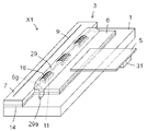
以下、サーマルヘッドX1について図1〜4を参照して説明する。図1は、サーマルヘッドX1の構成を概略的に示している。図2は、保護層25、および被覆層27を省略して示しており、被覆部材29は一点鎖線で示しており、配線導体6bの図示を省略している。
First Embodiment
Hereinafter, the thermal head X1 will be described with reference to FIGS. FIG. 1 schematically shows the configuration of the thermal head X1. In FIG. 2, the protective layer 25 and the covering layer 27 are omitted, and the covering member 29 is indicated by an alternate long and short dash line, and the wiring conductor 6b is omitted.

サーマルヘッドX1は、ヘッド基体3と、配線基板6と、放熱板1と、接着部材14と、導電部材16と、被覆部材29と、フレキシブル配線基板5(以下、FPC5と称する)と、コネクタ31とを有している。ヘッド基体3および配線基板6は、接着部材14により放熱板1に固定されている。駆動IC11は、配線基板6上に設けられており、導電部材16を介してヘッド基体3と電気的に接続されている。駆動IC11は、被覆部材29により封止されており、被覆部材29の一部は放熱板1上に配置されている。FPC5は、配線基板6と電気的に接続されており、コネクタ31を介して外部と電気的に接続されている。   The thermal head X 1 includes a head base 3, a wiring board 6, a heat sink 1, an adhesive member 14, a conductive member 16, a covering member 29, a flexible wiring board 5 (hereinafter referred to as an FPC 5), and a connector 31. And. The head base 3 and the wiring board 6 are fixed to the heat sink 1 by the bonding member 14. The drive IC 11 is provided on the wiring board 6 and is electrically connected to the head base 3 via the conductive member 16. The drive IC 11 is sealed by a covering member 29, and a part of the covering member 29 is disposed on the heat sink 1. The FPC 5 is electrically connected to the wiring substrate 6 and is electrically connected to the outside through the connector 31.

放熱板1は、平板形状をなしており、ヘッド基体3および配線基板6が載置されている。放熱板1は、例えば、銅、鉄またはアルミニウム等の金属材料で形成されており、ヘッド基体3の発熱部9で発生した熱のうち、印画に寄与しない熱を放熱する機能を有している。放熱板1は、金属材料により形成されているため、熱膨張係数が9〜11ppm/℃程度となっている。   The heat sink 1 has a flat plate shape, and the head base 3 and the wiring board 6 are mounted. The heat sink 1 is formed of, for example, a metal material such as copper, iron, or aluminum, and has a function of radiating the heat that does not contribute to the printing among the heat generated by the heat generating portion 9 of the head base 3. . Since the heat sink 1 is formed of a metal material, the thermal expansion coefficient is about 9 to 11 ppm / ° C.

ヘッド基体3は、平面視して、長方形状に形成されており、ヘッド基体3の基板7上にサーマルヘッドX1を構成する各部材が設けられている。ヘッド基体3は、外部より供給された電気信号に従い、記録媒体(図5参照)に印字を行う機能を有する。   The head substrate 3 is formed in a rectangular shape in plan view, and the respective members constituting the thermal head X 1 are provided on the substrate 7 of the head substrate 3. The head substrate 3 has a function of printing on a recording medium (see FIG. 5) in accordance with an electric signal supplied from the outside.

配線基板6は、図3に示すように、基材6aと、配線導体6bと、カバー部材6cとを有している。配線基板6は、主走査方向に長い矩形板形状をなしており、矩形状の主面に駆動IC11が載置されている。駆動IC11からは、ボンディングワイヤにより形成された導電部材16が引き出されており、導電部材16が、ヘッド基体3に電気的に接続されている。なお、図示していないが、駆動IC11からは配線基板6に向けて導電部材16が引き出されており、配線基板6に設けられた配線導体6bと電気的に接続されている。   As shown in FIG. 3, the wiring board 6 has a base 6a, a wiring conductor 6b, and a cover member 6c. The wiring board 6 has a rectangular plate shape long in the main scanning direction, and the drive IC 11 is mounted on the rectangular main surface. A conductive member 16 formed of a bonding wire is drawn out from the drive IC 11, and the conductive member 16 is electrically connected to the head base 3. Although not shown, the conductive member 16 is drawn from the drive IC 11 toward the wiring substrate 6 and is electrically connected to the wiring conductor 6 b provided on the wiring substrate 6.

配線導体6bは、基材6a上にパターニングされており、配線導体6bを介してFPC5とヘッド基体3とを電気的に接続している。配線基板6としては、硬質なリジッド基板、あるいはPCB等を例示することができる。そのため、配線基板6は、熱膨張係数が18〜20ppm/℃程度となっている。   The wiring conductor 6b is patterned on the base 6a, and electrically connects the FPC 5 and the head base 3 through the wiring conductor 6b. As the wiring board 6, a hard rigid board or a PCB can be exemplified. Therefore, the wiring board 6 has a thermal expansion coefficient of about 18 to 20 ppm / ° C.

FPC5は、基材5aと、配線導体5bと、カバー部材5cとを有している。基材5aおよびカバー部材5cは、可撓性のあるフレキシブルプリント配線板により形成されてお
り、配線導体5bは、金属の薄膜により形成されている。コネクタ31は、FPC5に電気的に接続されており、FPC5と外部電源とを電気的に接続している。
The FPC 5 includes a base 5 a, a wiring conductor 5 b, and a cover member 5 c. The base 5 a and the cover member 5 c are formed of a flexible printed wiring board having flexibility, and the wiring conductor 5 b is formed of a thin film of metal. The connector 31 is electrically connected to the FPC 5 and electrically connects the FPC 5 to an external power supply.

図3に示すように、配線基板6とFPC5とは、接合部材23により接合されている。接合部材23は、例えば、はんだ、あるいは電気絶縁性の樹脂中に導電性粒子が混入された異方性導電接着剤等を例示することができる。なお、接合部材23と配線導体5bとの間にNi、Au、あるいはPdによるめっき層(不図示)を設けてもよい。   As shown in FIG. 3, the wiring substrate 6 and the FPC 5 are bonded by a bonding member 23. The bonding member 23 can be exemplified by, for example, a solder or an anisotropic conductive adhesive in which conductive particles are mixed in an electrically insulating resin. A plated layer (not shown) of Ni, Au or Pd may be provided between the bonding member 23 and the wiring conductor 5b.

接着部材14は、放熱板1上に配置されており、ヘッド基体3および配線基板6と、放熱板1とを接合している。それにより、ヘッド基体3、配線基板6、および放熱板1は、一体化されている。接着部材14としては、両面テープ、あるいは樹脂性の接着剤を例示することができる。   The bonding member 14 is disposed on the heat dissipation plate 1 and joins the head base 3 and the wiring board 6 to the heat dissipation plate 1. Thus, the head base 3, the wiring substrate 6, and the heat sink 1 are integrated. The adhesive member 14 can be exemplified by a double-sided tape or a resinous adhesive.

被覆部材29は、駆動IC11を被覆するように設けられており、主走査方向に長く形成されている。被覆部材29は、ヘッド基体3、配線基板6、および放熱板1上に設けられており、駆動IC11を保護するとともに、ヘッド基体3、配線基板6、および放熱板1を接合している。被覆部材29は、例えば、エポキシ系の熱硬化性の樹脂、紫外線硬化性の樹脂、あるいは可視光硬化性の樹脂により形成することができる。   The covering member 29 is provided to cover the drive IC 11 and is formed to be long in the main scanning direction. The covering member 29 is provided on the head base 3, the wiring board 6 and the heat dissipation plate 1, and protects the drive IC 11 and joins the head base 3, the wiring board 6 and the heat dissipation plate 1. The covering member 29 can be formed of, for example, an epoxy thermosetting resin, an ultraviolet curable resin, or a visible light curable resin.

以下、ヘッド基体3を構成する各部材について、図2,3を用いて説明する。   Hereinafter, each member which comprises the head base 3 is demonstrated using FIG.2, 3. FIG.

基板7は、放熱板1上に配置されており、平面視して、矩形状をなしている。そのため、基板7は、一方の長辺7aと、他方の長辺7bと、一方の短辺7cと、他方の短辺7dとを有している。基板7は、例えば、アルミナセラミックス等の電気絶縁性材料あるいは単結晶シリコン等の半導体材料等によって形成されている。そのため、基板7は、熱膨張係数が6〜8ppm/℃程度となっており、放熱板1よりも熱膨張係数が小さくなっている。   The substrate 7 is disposed on the heat sink 1 and has a rectangular shape in plan view. Therefore, the substrate 7 has one long side 7 a, the other long side 7 b, one short side 7 c, and the other short side 7 d. The substrate 7 is made of, for example, an electrically insulating material such as alumina ceramic or a semiconductor material such as single crystal silicon. Therefore, the thermal expansion coefficient of the substrate 7 is approximately 6 to 8 ppm / ° C., and the thermal expansion coefficient is smaller than that of the heat sink 1.

基板7上には蓄熱層13が設けられている。蓄熱層13は、基板7の上方へ向けて突出した隆起部13aを備えている。隆起部13aは、基板7の一方の長辺7aに隣り合うように配置されており、複数の発熱部9の配列方向に沿って帯状に延び、断面が略半楕円形状をなしている。また、隆起部13aは、印画する記録媒体P(図7参照)を、発熱部9上に形成された保護層25に良好に押し当てるように機能している。隆起部13aは、基板7からの高さが15〜90μmで設けられることが好ましい。   A heat storage layer 13 is provided on the substrate 7. The heat storage layer 13 includes a raised portion 13 a protruding toward the upper side of the substrate 7. The protruding portion 13a is disposed adjacent to one long side 7a of the substrate 7, extends in a strip along the arrangement direction of the plurality of heat generating portions 9, and has a substantially semi-elliptical cross section. In addition, the protruding portion 13 a functions to well press the recording medium P (see FIG. 7) to be printed against the protective layer 25 formed on the heat generating portion 9. It is preferable that the height of the raised portion 13 a from the substrate 7 be 15 to 90 μm.

蓄熱層13は、熱伝導性の低いガラスで形成されており、発熱部9で発生する熱の一部を一時的に蓄積する。そのため、発熱部9の温度を上昇させるのに要する時間を短くすることができ、サーマルヘッドX1の熱応答特性を高めるように機能する。蓄熱層13は、例えば、ガラス粉末に適当な有機溶剤を混合して得た所定のガラスペーストを従来周知のスクリーン印刷等によって基板7の上面に塗布し、これを焼成することで形成される。   The heat storage layer 13 is formed of glass with low thermal conductivity, and temporarily accumulates part of the heat generated by the heat generating portion 9. Therefore, the time required to raise the temperature of the heat generating portion 9 can be shortened, and the heat response characteristic of the thermal head X1 can be enhanced. The heat storage layer 13 is formed, for example, by applying a predetermined glass paste obtained by mixing a suitable organic solvent with a glass powder on the upper surface of the substrate 7 by screen printing or the like known in the related art and baking it.

電気抵抗層15は、基板7の上面および蓄熱層13の上面に設けられており、電気抵抗層15上には、ヘッド基体3を構成する各種電極が設けられている。電気抵抗層15は、ヘッド基体3を構成する各種電極と同形状にパターニングされており、共通電極17と個別電極19との間に電気抵抗層15が露出した露出領域を有する。各露出領域は発熱部9を構成しており、隆起部13a上に列状に配置されている。   The electric resistance layer 15 is provided on the upper surface of the substrate 7 and the upper surface of the heat storage layer 13, and various electrodes constituting the head substrate 3 are provided on the electric resistance layer 15. The electric resistance layer 15 is patterned in the same shape as the various electrodes constituting the head substrate 3 and has an exposed region between the common electrode 17 and the individual electrode 19 in which the electric resistance layer 15 is exposed. Each exposed area constitutes a heat generating portion 9 and is arranged in a row on the raised portion 13a.

複数の発熱部9は、説明の便宜上、図2では簡略化して記載しているが、例えば、100dpi〜2400dpi(dot per inch)等の密度で配置される。電気抵抗層15は、例えば、TaN系、TaSiO系、TaSiNO系、TiSiO系、TiSiCO系また
はNbSiO系等の電気抵抗の比較的高い材料によって形成されている。そのため、発熱部9に電圧が印加されたときに、ジュール発熱によって発熱部9が発熱する。
The plurality of heat generating portions 9 are described in a simplified manner in FIG. 2 for convenience of explanation, but are arranged at a density of, for example, 100 dpi to 2400 dpi (dot per inch). The electric resistance layer 15 is formed of, for example, a material having a relatively high electric resistance, such as a TaN system, a TaSiO system, a TaSiNO system, a TiSiO system, a TiSiCO system, or a NbSiO system. Therefore, when a voltage is applied to the heat generating portion 9, the heat generating portion 9 generates heat by Joule heat generation.

共通電極17は、主配線部17aと、副配線部17bと、リード部17cと、接続部17dとを備えている。共通電極17は、複数の発熱部9と、コネクタ31とを電気的に接続している。主配線部17aは、基板7の一方の長辺7aに沿って延びている。副配線部17bは、基板7の一方の短辺7cおよび他方の短辺7dのそれぞれに沿って延びている。リード部17cは、主配線部17aから各発熱部9に向かって個別に延びている。接続部17dは、導電部材16(図1)に電気的に接続されている。   The common electrode 17 includes a main wiring portion 17a, a sub wiring portion 17b, a lead portion 17c, and a connection portion 17d. The common electrode 17 electrically connects the plurality of heat generating portions 9 and the connector 31. The main wiring portion 17 a extends along one long side 7 a of the substrate 7. The sub wiring portion 17 b extends along each of the short side 7 c and the other short side 7 d of the substrate 7. The lead portions 17 c individually extend from the main wiring portion 17 a toward the heat generating portions 9. The connection portion 17 d is electrically connected to the conductive member 16 (FIG. 1).

複数の個別電極19は、発熱部9と駆動IC11との間を電気的に接続している。また、個別電極19は、複数の発熱部9を複数の群に分けており、各群の発熱部9と各群に対応して設けられた駆動IC11とを電気的に接続している。個別電極19の端部には、パッド4が設けられている。パッド4は、上方に配置された駆動IC11と、接合部材23を介して電気的に接続されている。   The plurality of individual electrodes 19 electrically connect between the heat generating portion 9 and the drive IC 11. The individual electrodes 19 divide the plurality of heat generating portions 9 into a plurality of groups, and electrically connect the heat generating portions 9 of each group to the drive ICs 11 provided corresponding to the respective groups. A pad 4 is provided at the end of the individual electrode 19. The pad 4 is electrically connected to the drive IC 11 disposed above via the bonding member 23.

複数のIC−IC接続電極26は、隣り合う駆動IC11を電気的に接続している。複数のIC−IC接続電極26は、それぞれIC−コネクタ接続電極21に対応するように設けられており、各種信号を隣り合う駆動IC11に伝えている。   The plurality of IC-IC connection electrodes 26 electrically connect adjacent drive ICs 11. The plurality of IC-IC connection electrodes 26 are provided to correspond to the IC-connector connection electrodes 21, respectively, and transmit various signals to the adjacent drive ICs 11.

上記のヘッド基体3を構成する各種電極は、例えば、各々を構成する材料層を蓄熱層13上に、例えばスパッタリング法等の従来周知の薄膜成形技術によって順次積層した後、積層体を従来周知のフォトエッチング等を用いて所定のパターンに加工することにより形成される。なお、ヘッド基体3を構成する各種電極は、同じ工程によって同時に形成することができる。   The various electrodes constituting the head substrate 3 are, for example, sequentially laminating the material layers constituting each on the heat storage layer 13 by the conventional thin film forming technology such as sputtering, for example, and then the laminated body is known conventionally. It is formed by processing into a predetermined pattern using photo etching or the like. The various electrodes constituting the head substrate 3 can be formed simultaneously by the same process.

駆動IC11は、図2に示すように、複数の発熱部9の各群に対応して配置されている。図3に示すように、駆動IC11は、個別電極19のパッド4と導電部材16を介して電気的に接続されており、配線導体6bと導電部材16を介して電気的に接続されている。駆動IC11は、各発熱部9の通電状態を制御する機能を有している。駆動IC11としては、内部に複数のスイッチング素子を有する切替部材を用いればよい。   As shown in FIG. 2, the drive IC 11 is disposed corresponding to each group of the plurality of heat generating portions 9. As shown in FIG. 3, the drive IC 11 is electrically connected to the pad 4 of the individual electrode 19 via the conductive member 16 and electrically connected to the wiring conductor 6 b via the conductive member 16. The drive IC 11 has a function of controlling the energization state of each heat generating portion 9. As the drive IC 11, a switching member having a plurality of switching elements inside may be used.

図3に示すように、基板7上に設けられた蓄熱層13上には、発熱部9、共通電極17の一部および個別電極19の一部を被覆する保護層25が形成されている。   As shown in FIG. 3, on the heat storage layer 13 provided on the substrate 7, a protective layer 25 that covers the heating portion 9, a part of the common electrode 17 and a part of the individual electrode 19 is formed.

保護層25は、発熱部9、共通電極17および個別電極19の被覆した領域を、大気中に含まれている水分等の付着による腐食、あるいは印画する記録媒体との接触による摩耗から保護するためのものである。保護層25は、SiN、SiO、SiON、SiC、あるいはダイヤモンドライクカーボン等を用いて形成することができ、保護層25を単層で構成してもよいし、これらの層を積層して構成してもよい。このような保護層25はスパッタリング法等の薄膜形成技術あるいはスクリーン印刷等の厚膜形成技術を用いて作製することができる。 The protective layer 25 protects the area covered with the heat generating portion 9, the common electrode 17 and the individual electrode 19 from corrosion due to adhesion of moisture contained in the atmosphere or abrasion due to contact with a recording medium to be printed. belongs to. The protective layer 25 can be formed using SiN, SiO 2 , SiON, SiC, diamond like carbon or the like, and the protective layer 25 may be formed as a single layer, or these layers are laminated. You may Such a protective layer 25 can be manufactured using a thin film forming technique such as a sputtering method or a thick film forming technique such as screen printing.

また、図3に示すように、基板7上には、保護層25および個別電極19を部分的に被覆する被覆層27が設けられている。被覆層27は、被覆した領域を、大気との接触による酸化、あるいは大気中に含まれている水分等の付着による腐食から保護する機能を有する。   Further, as shown in FIG. 3, a covering layer 27 partially covering the protective layer 25 and the individual electrodes 19 is provided on the substrate 7. The coating layer 27 has a function of protecting the coated region from oxidation due to contact with the atmosphere or corrosion due to adhesion of moisture and the like contained in the atmosphere.

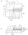
図4を用いて、配線基板6と、ヘッド基体3と、放熱板1との接合について説明する。なお、図4は、放熱板1と、接着部材14と、基板7と、配線基板6と、被覆部材29と
を示しており、その他の部材は省略して示している。また、配線基板6において、基材6a、配線導体6b、およびカバー部材6cの構成を省略して示している。また、図4(a)では、理解を容易にするために、被覆部材29は斑点で示している。
The bonding of the wiring substrate 6, the head base 3 and the heat sink 1 will be described with reference to FIG. 4 shows the heat sink 1, the bonding member 14, the substrate 7, the wiring substrate 6, and the covering member 29, and other members are omitted. Moreover, in the wiring board 6, the structure of the base 6a, the wiring conductor 6b, and the cover member 6c is abbreviate | omitted and shown. Also, in FIG. 4A, the covering member 29 is shown as spots for easy understanding.

基板7および配線基板6は、接着部材14により放熱板1上に接合されている。基板7および配線基板6は、副走査方向に並んで配置されており、主走査方向に長く形成されている。基板7の主走査方向の長さは、配線基板6の主走査方向のおける長さよりも長く構成されており、基板7の他方の長辺7cの一部と、他方の短辺7dとが、被覆部材29から露出している。   The substrate 7 and the wiring substrate 6 are bonded on the heat dissipation plate 1 by the bonding member 14. The substrate 7 and the wiring substrate 6 are arranged side by side in the sub scanning direction, and are formed long in the main scanning direction. The length of the substrate 7 in the main scanning direction is longer than the length of the wiring substrate 6 in the main scanning direction, and a part of the other long side 7 c of the substrate 7 and the other short side 7 d are It is exposed from the covering member 29.

配線基板6は、主面が矩形状をなしており、主走査方向に沿った第1側面6dと、副走査方向に沿った第2側面6eとを有している。第1側面6dは、基板7の他方の長辺7cに向かい合うように配置されている。   The wiring substrate 6 has a rectangular main surface, and has a first side surface 6 d along the main scanning direction and a second side surface 6 e along the sub-scanning direction. The first side surface 6 d is disposed to face the other long side 7 c of the substrate 7.

第2側面6eは、直線部6fと、切欠部6gとを有している。直線部6fは、切欠部6gと第1側面6dとを連結しており、副走査方向に延びて形成されている。切欠部6gは、第2側面6eの一部を切欠くように形成されており、平面視して、半円形状をなしている。切欠部6gは、第1側面6dと離間した状態で設けられている。   The second side face 6e has a straight portion 6f and a notch 6g. The linear portion 6 f connects the cutout portion 6 g and the first side surface 6 d and is formed to extend in the sub-scanning direction. The notch 6g is formed so as to cut out a part of the second side face 6e, and has a semicircular shape in plan view. The notch 6g is provided in a state of being separated from the first side surface 6d.

被覆部材29は、ワイヤ(図1参照)を被覆するように設けられており、基板7および配線基板6上に形成されている。配線基板6上に配置された被覆部材29の一部は、図4(b)に示すように、切欠部6gに流れ込んでおり、切欠部6gを通じて放熱板1上に流動被覆部材29aとして流れ出している。それにより、流動被覆部材29aが放熱板1と接触されており、接着部材14に加えて流動被覆部材29aにより配線基板6を放熱板1に接合することができ、配線基板6の接合強度を向上させることができる。   The covering member 29 is provided to cover the wire (see FIG. 1), and is formed on the substrate 7 and the wiring substrate 6. A part of the covering member 29 disposed on the wiring substrate 6 flows into the notch 6g as shown in FIG. 4B, and flows out onto the heat sink 1 as a flow covering member 29a through the notch 6g. There is. Thereby, the fluid covering member 29a is in contact with the heat dissipation plate 1, and the wiring substrate 6 can be joined to the heat dissipation plate 1 by the fluid covering member 29a in addition to the bonding member 14, and the bonding strength of the wiring substrate 6 is improved. It can be done.

ここで、放熱板1は、基板7よりも熱膨張係数が大きく、サーマルヘッドX1の製造時あるいは駆動時の温度サイクルにより、基板7の側面に応力が集中する問題がある。特に、基板7が主走査方向に長く形成されている場合、主走査方向における両端部の側面、すなわち他方の長辺7cを構成する側面、および他方の長辺7dを構成する側面に大きな応力が生じることとなる。そのため、被覆部材29が、基板7の側面に隣り合う空間8に配置されると、被覆部材29に応力が集中することとなり、被覆部材29にクラックが生じるおそれがある。   Here, the heat dissipation plate 1 has a thermal expansion coefficient larger than that of the substrate 7, and there is a problem that stress is concentrated on the side surface of the substrate 7 due to the temperature cycle at the time of manufacturing or driving the thermal head X1. In particular, when the substrate 7 is formed long in the main scanning direction, a large stress is generated on the side surfaces of both ends in the main scanning direction, that is, the side surfaces forming the other long side 7c and the side surfaces forming the other long side 7d. It will occur. Therefore, when the covering member 29 is disposed in the space 8 adjacent to the side surface of the substrate 7, stress is concentrated on the covering member 29, and a crack may occur in the covering member 29.

これに対して、配線基板6が第1側面6dから離間した切欠部6gを有しており、配線基板6上に設けられた被覆部材29の一部は、切欠部6gの毛細管現象により切欠部6g上に設けられ、切欠部6g上に設けられた流動被覆部材29aが、放熱板1と接合されている。そのため、配線基板6の接合強度を向上させることができるとともに、被覆部材29の基板7側の空間8への流入を低減することができ、被覆部材29への応力集中を低減することができる。その結果、被覆部材29の接合強度を向上させつつ、被覆部材29におけるクラック発生を低減することができる。   On the other hand, the wiring board 6 has the notch 6g separated from the first side face 6d, and a part of the covering member 29 provided on the wiring board 6 is a notch due to the capillary phenomenon of the notch 6g. A fluid covering member 29 a provided on 6 g and provided on the notch 6 g is joined to the heat sink 1. Therefore, the bonding strength of the wiring substrate 6 can be improved, the inflow of the covering member 29 into the space 8 on the substrate 7 side can be reduced, and the stress concentration on the covering member 29 can be reduced. As a result, it is possible to reduce the occurrence of cracks in the covering member 29 while improving the bonding strength of the covering member 29.

なお、切欠部6g上に設けられた流動被覆部材29aと、放熱板1とが接合されているとは、流動被覆部材29aと放熱板1とが接着部材14を介して接合されていることを含んでいる。   The fact that the flow covering member 29a provided on the notch 6g and the heat dissipation plate 1 are joined means that the flow covering member 29a and the heat dissipation plate 1 are joined via the bonding member 14 It contains.

配線基板6の第2側面6eは、平面視して、切欠部6gと基板7との間に直線部6fが設けられている。この直線部6fは、配線基板6の第2側面6eと主面の交差線であり、角部となっている。そのため、図4(c)に示すように、配線基板6上に設けられた被覆部材29は、配線基板6上から基板7上の空間8側に流動しようとする際に、直線部6f
上で表面張力が働き、直線部6f上で堰きとめられることとなる。それゆえ、基板7側の空間8に、被覆部材29が設けられ難くすることができる。
The second side surface 6 e of the wiring substrate 6 is provided with a linear portion 6 f between the cutout portion 6 g and the substrate 7 in plan view. The straight portion 6 f is a cross line between the second side surface 6 e of the wiring substrate 6 and the main surface, and is a corner portion. Therefore, as shown in FIG. 4C, when the covering member 29 provided on the wiring substrate 6 is going to flow from the wiring substrate 6 to the space 8 side on the substrate 7, the straight portion 6f
The surface tension acts on the upper side, and it is caught on the straight portion 6f. Therefore, the covering member 29 can be made difficult to be provided in the space 8 on the substrate 7 side.

すなわち、被覆部材29は、主走査方向に流動し直線部6fに到達すると、直線部6f以降は、配線基板6が設けられていないため、被覆部材29は、配線基板6よりも濡れ性の低い空気に囲まれる構成となる。その結果、被覆部材29に表面張力が働き、配線基板6上から基板7上の空間8に流れにくくなる。それゆえ、被覆部材29を直線部6fにより堰きとめることができる。   That is, when the covering member 29 flows in the main scanning direction and reaches the linear portion 6 f, the wiring board 6 is not provided in the linear portion 6 f and thereafter, so the covering member 29 has lower wettability than the wiring board 6. It will be surrounded by the air. As a result, surface tension acts on the covering member 29 and it becomes difficult to flow from above the wiring substrate 6 to the space 8 above the substrate 7. Therefore, the covering member 29 can be stopped by the straight portion 6f.

直線部6fの副走査方向における長さは、図4(a)に示すように、切欠部6gと基板7との距離よりも長くなっている。そのため、切欠部6gにより放熱板1上に、流動被覆部材29aが配置されても、基板7との距離が十分にあり、基板7側の空間8に流れ込みにくいこととなる。その結果、被覆部材29の接合強度を向上させつつ、被覆部材29におけるクラックの発生を低減することができる。   The length of the linear portion 6f in the sub scanning direction is longer than the distance between the notch 6g and the substrate 7 as shown in FIG. 4A. Therefore, even if the flow covering member 29a is disposed on the heat sink 1 by the notch 6g, the distance to the substrate 7 is sufficient, and it is difficult to flow into the space 8 on the substrate 7 side. As a result, it is possible to reduce the occurrence of cracks in the covering member 29 while improving the bonding strength of the covering member 29.

直線部6fの副走査方向における長さは、例えば、0.3〜1.5mmとすることができ、切欠部6gと基板7との距離は、例えば、0.3〜1.5mmとすることができる。また、基板7の副走査方向における長さが、0.3〜1.0mmの時、被覆部材29の副走査方向における長さは、例えば、1.5〜3.5mmとすることができる。   The length of the linear portion 6f in the sub scanning direction may be, for example, 0.3 to 1.5 mm, and the distance between the notch 6g and the substrate 7 may be, for example, 0.3 to 1.5 mm. Can. When the length of the substrate 7 in the sub scanning direction is 0.3 to 1.0 mm, the length of the covering member 29 in the sub scanning direction can be, for example, 1.5 to 3.5 mm.

サーマルヘッドX1の配線基板6と、ヘッド基体3と、放熱板1との接合について説明する。   The bonding of the wiring substrate 6 of the thermal head X1, the head base 3 and the heat dissipation plate 1 will be described.

まず、駆動IC11(図1参照)が実装された配線基板6の第2側面6eに、ドリル等により切欠部6gを形成する。次に、放熱板1に接着部材14を接合する。次に、接着部材14上に基板7および配線基板6を載置する。この際、基板7の他方の長辺7cにより形成される側面と、配線基板6の第1側面6dとを向かい合わせて載置する。   First, a notch 6g is formed by a drill or the like on the second side 6e of the wiring substrate 6 on which the drive IC 11 (see FIG. 1) is mounted. Next, the bonding member 14 is bonded to the heat sink 1. Next, the substrate 7 and the wiring substrate 6 are placed on the bonding member 14. At this time, the side surface formed by the other long side 7 c of the substrate 7 and the first side surface 6 d of the wiring substrate 6 are placed facing each other.

次に、導電部材16(図1参照)を被覆するように、被覆部材29をディスペンサーにより塗布する。被覆部材29は、主走査方向にディスペンサーのヘッドを動かしながら、樹脂を塗布して形成される。ディスペンサーのヘッドは、切欠部6gに被覆部材が設けられるように、第2側面6e近傍では、塗布する被覆部材の量を多くする。塗布された被覆部材29の一部は、毛細管現象により切欠部6gに導かれて、流動被覆部材29aが放熱板1上に形成される。続いて、被覆部材29を乾燥、硬化して、配線基板6と、ヘッド基体3と、放熱板1とを接合することができる。   Next, the covering member 29 is applied by a dispenser so as to cover the conductive member 16 (see FIG. 1). The covering member 29 is formed by applying a resin while moving the dispenser head in the main scanning direction. The head of the dispenser increases the amount of the covering member to be applied near the second side face 6e so that the covering member is provided in the notch 6g. A part of the applied covering member 29 is led to the notch 6 g by capillary action, and a fluid covering member 29 a is formed on the heat dissipation plate 1. Subsequently, the covering member 29 can be dried and cured to bond the wiring board 6, the head base 3, and the heat dissipation plate 1.

次に、サーマルプリンタZ1について、図5を参照しつつ説明する。   Next, the thermal printer Z1 will be described with reference to FIG.

図5に示すように、本実施形態のサーマルプリンタZ1は、上述のサーマルヘッドX1と、搬送機構40と、プラテンローラ50と、電源装置60と、制御装置70とを備えている。サーマルヘッドX1は、サーマルプリンタZ1の筐体(不図示)に設けられた取付部材80の取付面80aに取り付けられている。なお、サーマルヘッドX1は、後述する記録媒体Pの搬送方向Sに直交する方向である主走査方向に沿うようにして、取付部材80に取り付けられている。   As shown in FIG. 5, the thermal printer Z1 of the present embodiment includes the above-described thermal head X1, a transport mechanism 40, a platen roller 50, a power supply device 60, and a control device 70. The thermal head X1 is mounted on a mounting surface 80a of a mounting member 80 provided on a housing (not shown) of the thermal printer Z1. The thermal head X1 is attached to the mounting member 80 along the main scanning direction which is a direction perpendicular to the conveyance direction S of the recording medium P described later.

搬送機構40は、駆動部(不図示)と、搬送ローラ43,45,47,49とを有している。搬送機構40は、感熱紙、インクが転写される受像紙等の記録媒体Pを図5の矢印S方向に搬送して、サーマルヘッドX1の複数の発熱部9上に位置する保護層25上に搬送するためのものである。駆動部は、搬送ローラ43,45,47,49を駆動させる機能を有しており、例えば、モータを用いることができる。搬送ローラ43,45,47,
49は、例えば、ステンレス等の金属からなる円柱状の軸体43a,45a,47a,49aを、ブタジエンゴム等からなる弾性部材43b,45b,47b,49bにより被覆して構成することができる。なお、図示しないが、記録媒体Pがインクが転写される受像紙等の場合は、記録媒体PとサーマルヘッドX1の発熱部9との間に、記録媒体Pとともにインクフィルムを搬送する。
The transport mechanism 40 has a drive unit (not shown) and transport rollers 43, 45, 47 and 49. Conveying mechanism 40 conveys recording medium P such as thermal paper, image receiving paper to which ink is transferred in the direction of arrow S in FIG. 5, and places protective layer 25 located on heat generating portions 9 of thermal head X1. It is for carrying. The drive unit has a function of driving the transport rollers 43, 45, 47, and 49, and for example, a motor can be used. Conveying rollers 43, 45, 47,
For example, 49 can be configured by covering cylindrical shaft bodies 43a, 45a, 47a, 49a made of metal such as stainless steel with elastic members 43b, 45b, 47b, 49b made of butadiene rubber or the like. Although not shown, when the recording medium P is an image receiving paper or the like to which the ink is transferred, the ink film is conveyed together with the recording medium P between the recording medium P and the heat generating portion 9 of the thermal head X1.

プラテンローラ50は、記録媒体PをサーマルヘッドX1の発熱部9上に位置する保護膜25上に押圧する機能を有する。プラテンローラ50は、記録媒体Pの搬送方向Sに直交する方向に沿って延びるように配置され、記録媒体Pを発熱部9上に押圧した状態で回転可能となるように両端部が支持固定されている。プラテンローラ50は、例えば、ステンレス等の金属からなる円柱状の軸体50aを、ブタジエンゴム等からなる弾性部材50bにより被覆して構成することができる。   The platen roller 50 has a function of pressing the recording medium P onto the protective film 25 located on the heat generating portion 9 of the thermal head X1. The platen roller 50 is disposed to extend along a direction orthogonal to the conveyance direction S of the recording medium P, and both ends are supported and fixed so that the recording medium P can be rotated in a state of being pressed onto the heat generating portion 9 ing. The platen roller 50 can be configured, for example, by covering a cylindrical shaft 50a made of metal such as stainless steel with an elastic member 50b made of butadiene rubber or the like.

電源装置60は、上記のようにサーマルヘッドX1の発熱部9を発熱させるための電流および駆動IC11を動作させるための電流を供給する機能を有している。制御装置70は、上記のようにサーマルヘッドX1の発熱部9を選択的に発熱させるために、駆動IC11の動作を制御する制御信号を駆動IC11に供給する機能を有している。   As described above, the power supply device 60 has a function of supplying a current for heating the heating portion 9 of the thermal head X1 and a current for operating the drive IC 11. The control device 70 has a function of supplying a control signal for controlling the operation of the drive IC 11 to the drive IC 11 in order to cause the heat generating portion 9 of the thermal head X 1 to selectively generate heat as described above.

サーマルプリンタZ1は、プラテンローラ50によって記録媒体PをサーマルヘッドX1の発熱部9上に押圧しつつ、搬送機構40によって記録媒体Pを発熱部9上に搬送しながら、電源装置60および制御装置70によって発熱部9を選択的に発熱させることにより、記録媒体Pに所定の印画を行う。なお、記録媒体Pが受像紙等の場合は、記録媒体Pとともに搬送されるインクフィルム(不図示)のインクを記録媒体Pに熱転写することによって、記録媒体Pへの印画を行う。   While the thermal printer Z1 presses the recording medium P onto the heat generating portion 9 of the thermal head X1 by the platen roller 50, the power source device 60 and the control device 70 transport the recording medium P onto the heat generating portion 9 by the transport mechanism 40. Thus, predetermined heating is performed on the recording medium P by selectively heating the heat generating portion 9. When the recording medium P is an image receiving paper or the like, printing on the recording medium P is performed by thermally transferring the ink of an ink film (not shown) conveyed together with the recording medium P onto the recording medium P.

<第2の実施形態>
図6を用いてサーマルヘッドX2について説明する。なお、サーマルヘッドX1と同一の部材については同じ符号を付しており、以下同様とする。なお、図6は、図4と同様に、放熱板1と、接着部材14と、基板7と、配線基板106と、被覆部材129とを示しており、その他の部材は省略して示している。また、図4と同様に、図6(a)では、被覆部材129を斑点で示している。
Second Embodiment
The thermal head X2 will be described with reference to FIG. The same members as those of the thermal head X1 are denoted by the same reference numerals, and the same applies hereinafter. 6 shows the heat sink 1, the bonding member 14, the substrate 7, the wiring board 106, and the covering member 129 as in FIG. 4, and other members are omitted. . Further, in the same manner as in FIG. 4, the covering member 129 is indicated by spots in FIG.

配線基板106は、基材106aと、配線導体106bと、カバー部材106cとにより形成されており、第1側面106dと、第2側面106eと、主面に形成された凹部110とを有している。   The wiring board 106 is formed of a base 106a, a wiring conductor 106b, and a cover member 106c, and has a first side 106d, a second side 106e, and a recess 110 formed on the main surface. There is.

第1側面106dは、基板7の他方の長辺7cにより形成される側面と向かい合うように配置されている。第2側面106eは、直線部106fと、切欠部106gとを有している。   The first side surface 106 d is disposed to face the side surface formed by the other long side 7 c of the substrate 7. The second side surface 106e has a straight portion 106f and a notch 106g.

凹部110は、第1側面106dおよび第2側面106eから離間した状態で、配線基板106の主面に設けられており、配線基板106の上面が凹むように設けられている。そのため、凹部110の縁は、第1側面106dおよび第2側面106eと離間して配置されている。凹部110は、カバー部材106cを切欠いて形成されており、凹部110内には基材106aおよび配線導体112が露出している。   The recess 110 is provided on the main surface of the wiring board 106 in a state of being separated from the first side surface 106 d and the second side surface 106 e, and is provided such that the upper surface of the wiring board 106 is recessed. Therefore, the edge of the recess 110 is spaced apart from the first side surface 106 d and the second side surface 106 e. The recess 110 is formed by cutting out the cover member 106 c, and the base 106 a and the wiring conductor 112 are exposed in the recess 110.

配線基板106は、第2側面106eから離間した凹部110を有し、凹部110と基板7との距離が、切欠部106gと基板7との距離よりも短く構成されている。そのため、配線基板106上に設けられた被覆部材129が、配線基板106上から基板7上の空間8側に流動しようとした際に、凹部110の縁上で表面張力が働き、図6(a)に示す
ように、凹部110の縁上で堰きとめられることとなる。それゆえ、基板7側の空間8への被覆部材129の流入を低減することができる。
The wiring substrate 106 has a recess 110 separated from the second side surface 106 e, and the distance between the recess 110 and the substrate 7 is shorter than the distance between the notch 106 g and the substrate 7. Therefore, when the covering member 129 provided on the wiring substrate 106 tries to flow from the wiring substrate 106 to the space 8 side on the substrate 7, surface tension acts on the edge of the recess 110, as shown in FIG. ), It will be scooped on the edge of the recess 110. Therefore, the inflow of the covering member 129 into the space 8 on the substrate 7 side can be reduced.

また、配線基板106上に設けられた被覆部材129の塗布量が多かった場合においても、凹部110の内部に被覆部材129を収容することができ、余剰の被覆部材129が基板7側の空間8に流出することを低減できる。   Further, even when the coating amount of the covering member 129 provided on the wiring substrate 106 is large, the covering member 129 can be accommodated inside the recess 110, and the surplus covering member 129 is the space 8 on the substrate 7 side. Can be reduced.

さらに、余剰の被覆部材129が配線基板106の表面上にあると、被覆部材129の高さが高くなり、記録媒体P(図5参照)と接触する可能性があるが、凹部110の内部に被覆部材129を収容することで、被覆部材129の高さを低くできる。その結果、被覆部材129が記録媒体Pと接触する可能性を低減することができる。   Furthermore, when the excess covering member 129 is on the surface of the wiring substrate 106, the height of the covering member 129 is increased, and there is a possibility of contacting the recording medium P (see FIG. 5). By accommodating the covering member 129, the height of the covering member 129 can be lowered. As a result, the possibility of the covering member 129 coming into contact with the recording medium P can be reduced.

また、凹部110の縁と基板7との距離が、切欠部106gと基板7との距離よりも短く構成されているため、凹部110の縁上により堰きとめられた被覆部材129は、切欠部106gに流出しやすくなる。その結果、切欠部106gから放熱板1上に流動被覆部材129aが広がることとなり、配線基板106の接合強度を向上させることができる。   Further, since the distance between the edge of the recess 110 and the substrate 7 is shorter than the distance between the notch 106 g and the substrate 7, the covering member 129 captured by the edge of the recess 110 is the notch 106 g. It is easy to spill out. As a result, the flow coating member 129a spreads on the heat dissipation plate 1 from the notch portion 106g, and the bonding strength of the wiring board 106 can be improved.

以上、本発明の一実施形態について説明したが、本発明は上記実施形態に限定されるものではなく、その趣旨を逸脱しない限りにおいて種々の変更が可能である。例えば、第1の実施形態であるサーマルヘッドX1を用いたサーマルプリンタZ1を示したが、これに限定されるものではなく、サーマルヘッドX2をサーマルプリンタZ1に用いてもよい。   As mentioned above, although one Embodiment of this invention was described, this invention is not limited to the said embodiment, A various change is possible unless it deviates from the meaning. For example, although the thermal printer Z1 using the thermal head X1 according to the first embodiment is shown, the present invention is not limited to this, and the thermal head X2 may be used for the thermal printer Z1.

例えば、電気抵抗層15を薄膜形成することにより、発熱部9の薄い薄膜ヘッドを例示して示したが、これに限定されるものではない。各種電極をパターニングした後に、電気抵抗層15を厚膜形成することにより、発熱部9の厚い厚膜ヘッドに本発明を用いてもよい。   For example, although the thin thin film head of the heat generating portion 9 is illustrated by forming the electric resistance layer 15 as a thin film, it is not limited thereto. The present invention may be applied to a thick thick film head of the heat generating portion 9 by forming the electric resistance layer 15 as a thick film after patterning various electrodes.

また、発熱部9が基板7上に形成された平面ヘッドを例示して説明したが、発熱部9が基板7の端面に設けられた端面ヘッドに本発明を用いてもよい。   Further, although the planar head in which the heat generating portion 9 is formed on the substrate 7 is described as an example, the present invention may be applied to an end face head in which the heat generating portion 9 is provided on the end surface of the substrate 7.

また、蓄熱層13が隆起部13a以外の領域に、下地部を形成してもよい。また、蓄熱層13上に共通電極17および個別電極19を形成し、共通電極17と個別電極19との間の領域のみに電気抵抗層15を形成することにより、発熱部9を形成してもよい。   In addition, the base portion may be formed in the region where the heat storage layer 13 is other than the raised portion 13a. Further, even if the common electrode 17 and the individual electrode 19 are formed on the heat storage layer 13 and the electric resistance layer 15 is formed only in the region between the common electrode 17 and the individual electrode 19, the heating portion 9 is formed. Good.

X1〜X2 サーマルヘッド
Z1 サーマルプリンタ
1 放熱板
3 ヘッド基体
5 フレキシブル配線基板
6,106 配線基板
6a,106a 基材
6b,106b 配線導体
6c,106c カバー部材
6d,106d 第1側面
6e,106e第2側面
6f,106f直線部
6g,106g 切欠部
7 基板
9 発熱部
11 駆動IC
13 蓄熱層
14 接着部材
16 導電部材
17 共通電極
19 個別電極
23 接合部材
29,129 被覆部材
29a,129a 流動被覆部材
31 コネクタ
40 搬送機構
50 プラテンローラ

X1 to X2 thermal head Z1 thermal printer 1 heat dissipation plate 3 head substrate 5 flexible wiring substrate 6, 106 wiring substrate 6a, 106a substrate 6b, 106b wiring conductor 6c, 106c cover member 6d, 106d first side 6e, 106e second side 6f, 106f straight part 6g, 106g notched part 7 substrate 9 heat generating part 11 drive IC
Reference Signs List 13 heat storage layer 14 bonding member 16 conductive member 17 common electrode 19 individual electrode 23 bonding member 29, 129 covering member 29a, 129a fluid covering member 31 connector 40 conveying mechanism 50 platen roller

Claims (5)

基板、前記基板上に設けられた発熱部、および、前記基板上に設けられ、前記発熱部と電気的に接続された電極を有するヘッド基体と、
平面視して前記ヘッド基体に並んで位置し、前記電極と電気的に接続された配線導体を有する配線基板と、
前記ヘッド基体および前記配線基板の下方に配置された放熱板と、
前記電極および前記配線導体を電気的に接続するための導電部材と、
前記導電部材を被覆するとともに、前記基板の一部および前記配線基板の一部上に設けられた被覆部材と、を備え、
前記配線基板は、主面が矩形状をなしており、主走査方向に延び、前記ヘッド基体に面する第1側面と、副走査方向に延びる第2側面とを有しており、前記第2側面に前記第1側面と離間した切欠部が設けられており、
前記放熱板は、前放熱板上における、前記ヘッド基体よりも前記副走査方向、かつ、前記切欠部よりも前記基板側に位置する前記第2側面の前記主走査方向の重なる領域に、前記被覆部材がないことを特徴とするサーマルヘッド。
A substrate, a heat generating portion provided on the substrate, and a head base having an electrode provided on the substrate and electrically connected to the heat generating portion;
A wiring board having a wiring conductor positioned parallel to the head base in plan view and electrically connected to the electrode;
A heat dissipation plate disposed below the head base and the wiring substrate;
A conductive member for electrically connecting the electrode and the wiring conductor;
And covering the conductive member, and covering a portion of the substrate and a portion of the wiring substrate.
The main surface of the wiring substrate has a rectangular shape, and the wiring substrate has a first side surface facing the head base and a second side surface extending in the sub-scanning direction. The side surface is provided with a notch separated from the first side surface,
The heat sink, before Symbol radiator plate, said sub-scanning direction than the head substrate, and, in the main scanning direction of overlapping region of the second side surface located on the substrate side of the notch, the A thermal head characterized by having no covering member .
前記第2側面は、平面視して、前記切欠部と前記基板との間に直線部が設けられている、請求項1に記載のサーマルヘッド。   The thermal head according to claim 1, wherein the second side surface is provided with a straight portion between the notch and the substrate in plan view. 前記放熱板は、前記被覆部材の前記切欠部に相当する位置に、前記配線基板上に位置する前記被覆部材と繋がる前記被覆部材が位置する、請求項1または2に記載のサーマルヘッド。 The thermal head according to claim 1 or 2, wherein the heat radiation plate has the covering member connected to the covering member positioned on the wiring substrate at a position corresponding to the cutout portion of the covering member . 前記配線基板の前記主面に、前記第2側面から離間した凹部を有し、
前記凹部と前記基板との距離が、前記切欠部と前記基板との距離よりも短い、請求項1〜3のいずれか一項に記載のサーマルヘッド。
The main surface of the wiring substrate has a recess spaced from the second side surface,
The thermal head according to any one of claims 1 to 3, wherein a distance between the recess and the substrate is shorter than a distance between the notch and the substrate.
請求項1〜4のうちいずれか一項に記載のサーマルヘッドと、
前記発熱部上に記録媒体を搬送する搬送機構と、
前記発熱部上に前記記録媒体を押圧するプラテンローラと、を備えることを特徴とするサーマルプリンタ。
The thermal head according to any one of claims 1 to 4.
A transport mechanism for transporting a recording medium onto the heat generating portion;
And a platen roller for pressing the recording medium on the heat generating portion.
JP2015169885A 2015-08-29 2015-08-29 Thermal head and thermal printer Active JP6525822B2 (en)

Priority Applications (1)

Application Number Priority Date Filing Date Title
JP2015169885A JP6525822B2 (en) 2015-08-29 2015-08-29 Thermal head and thermal printer

Applications Claiming Priority (1)

Application Number Priority Date Filing Date Title
JP2015169885A JP6525822B2 (en) 2015-08-29 2015-08-29 Thermal head and thermal printer

Publications (2)

Publication Number Publication Date
JP2017043076A JP2017043076A (en) 2017-03-02
JP6525822B2 true JP6525822B2 (en) 2019-06-05

Family

ID=58209367

Family Applications (1)

Application Number Title Priority Date Filing Date
JP2015169885A Active JP6525822B2 (en) 2015-08-29 2015-08-29 Thermal head and thermal printer

Country Status (1)

Country Link
JP (1) JP6525822B2 (en)

Family Cites Families (6)

* Cited by examiner, † Cited by third party
Publication number Priority date Publication date Assignee Title
JPH05229161A (en) * 1992-02-19 1993-09-07 Hitachi Ltd Heat-sensitive recorder
JP2576467Y2 (en) * 1993-06-24 1998-07-09 アオイ電子株式会社 Thermal print head
KR0154823B1 (en) * 1995-06-21 1998-12-01 김광호 Thermal transfr recording element
JP2002370396A (en) * 2001-06-13 2002-12-24 Sii P & S Inc Thermal head unit and its manufacturing method
JP5670132B2 (en) * 2010-09-16 2015-02-18 東芝ホクト電子株式会社 Thermal print head and thermal printer
JP2012071467A (en) * 2010-09-28 2012-04-12 Kyocera Corp Thermal head and thermal printer including the same

Also Published As

Publication number Publication date
JP2017043076A (en) 2017-03-02

Similar Documents

Publication Publication Date Title
JP5836825B2 (en) Thermal head and thermal printer equipped with the same
JP6059412B1 (en) Thermal head and thermal printer
JP6431200B2 (en) Thermal head and thermal printer
JP6419006B2 (en) Thermal head and thermal printer
JP6130510B2 (en) Thermal head and thermal printer equipped with the same
JP6346108B2 (en) Thermal head and thermal printer
JP6526198B2 (en) Thermal head and thermal printer
JP2012071467A (en) Thermal head and thermal printer including the same
JP6525822B2 (en) Thermal head and thermal printer
JP2012071522A (en) Thermal head and thermal printer including the same
WO2015099149A1 (en) Thermal head and thermal printer
JP6525819B2 (en) Thermal head and thermal printer
JP5937309B2 (en) Thermal head and thermal printer equipped with the same
JP6426528B2 (en) Thermal head and thermal printer
JP6154338B2 (en) Thermal head and thermal printer
JP6290632B2 (en) Thermal head and thermal printer equipped with the same
JP6208564B2 (en) Thermal head and thermal printer
JP6927767B2 (en) Thermal head and thermal printer
JP6075634B2 (en) Thermal head and thermal printer equipped with the same
JP7444972B2 (en) Thermal head and thermal printer
JP6426541B2 (en) Thermal head and thermal printer
JP2012030380A (en) Thermal head and thermal printer equipped with the same
JP6401078B2 (en) Thermal head and thermal printer equipped with the same
JP6352799B2 (en) Thermal head and thermal printer
JP6199814B2 (en) Thermal head and thermal printer

Legal Events

Date Code Title Description
A621 Written request for application examination

Free format text: JAPANESE INTERMEDIATE CODE: A621

Effective date: 20180514

A977 Report on retrieval

Free format text: JAPANESE INTERMEDIATE CODE: A971007

Effective date: 20190109

A131 Notification of reasons for refusal

Free format text: JAPANESE INTERMEDIATE CODE: A131

Effective date: 20190115

A521 Written amendment

Free format text: JAPANESE INTERMEDIATE CODE: A523

Effective date: 20190315

TRDD Decision of grant or rejection written
A01 Written decision to grant a patent or to grant a registration (utility model)

Free format text: JAPANESE INTERMEDIATE CODE: A01

Effective date: 20190402

A61 First payment of annual fees (during grant procedure)

Free format text: JAPANESE INTERMEDIATE CODE: A61

Effective date: 20190507

R150 Certificate of patent or registration of utility model

Ref document number: 6525822

Country of ref document: JP

Free format text: JAPANESE INTERMEDIATE CODE: R150