JP6208564B2 - Thermal head and thermal printer - Google Patents

Thermal head and thermal printer Download PDF

Info

Publication number
JP6208564B2
JP6208564B2 JP2013246250A JP2013246250A JP6208564B2 JP 6208564 B2 JP6208564 B2 JP 6208564B2 JP 2013246250 A JP2013246250 A JP 2013246250A JP 2013246250 A JP2013246250 A JP 2013246250A JP 6208564 B2 JP6208564 B2 JP 6208564B2
Authority
JP
Japan
Prior art keywords
connector
substrate
heat generating
housing
electrode
Prior art date
Legal status (The legal status is an assumption and is not a legal conclusion. Google has not performed a legal analysis and makes no representation as to the accuracy of the status listed.)
Active
Application number
JP2013246250A
Other languages
Japanese (ja)
Other versions
JP2015104807A (en
Inventor
優奈 大久保
優奈 大久保
保光 山本
保光 山本
雅文 平山
雅文 平山
久利 高田
久利 高田
Current Assignee (The listed assignees may be inaccurate. Google has not performed a legal analysis and makes no representation or warranty as to the accuracy of the list.)
Kyocera Corp
Original Assignee
Kyocera Corp
Priority date (The priority date is an assumption and is not a legal conclusion. Google has not performed a legal analysis and makes no representation as to the accuracy of the date listed.)
Filing date
Publication date
Application filed by Kyocera Corp filed Critical Kyocera Corp
Priority to JP2013246250A priority Critical patent/JP6208564B2/en
Publication of JP2015104807A publication Critical patent/JP2015104807A/en
Application granted granted Critical
Publication of JP6208564B2 publication Critical patent/JP6208564B2/en
Active legal-status Critical Current
Anticipated expiration legal-status Critical

Links

Images

Description

本発明は、サーマルヘッドおよびサーマルプリンタに関する。   The present invention relates to a thermal head and a thermal printer.

従来、ファクシミリあるいはビデオプリンタ等の印画デバイスとして、種々のサーマルヘッドが提案されている。例えば、基板と、基板上に設けられた複数の発熱部と、基板上に設けられ、発熱部に電気的に接続された電極と、電極に電気的に接続された複数のコネクタピン、および複数のコネクタピンを収容するハウジングを有したコネクタと、コネクタピンと電極との接続部を被覆する被覆部材とを備えるものが知られている。(例えば、引用文献1参照)。   Conventionally, various thermal heads have been proposed as printing devices such as facsimiles and video printers. For example, a substrate, a plurality of heat generating portions provided on the substrate, an electrode provided on the substrate and electrically connected to the heat generating portion, a plurality of connector pins electrically connected to the electrodes, and a plurality There is known a connector including a connector having a housing that accommodates the connector pin and a covering member that covers a connection portion between the connector pin and the electrode. (For example, refer to cited document 1).

特開2004−148577号公報JP 2004-1458577 A

しかしながら、上述したサーマルヘッドでは、コネクタピンが被覆部材から一部露出しているため、コネクタピンが完全に封止されておらず、コネクタピンが劣化するおそれがある。そのため、コネクタピンを完全に封止するために、被覆部材をコネクタピン上に塗布する必要がある。   However, in the above-described thermal head, since the connector pins are partially exposed from the covering member, the connector pins are not completely sealed, and the connector pins may be deteriorated. Therefore, in order to completely seal the connector pin, it is necessary to apply a covering member on the connector pin.

ところが、上述したサーマルヘッドでは、隣り合うコネクタピン同士の間に隙間が生じており、隙間から被覆部材が下方に流出してしまいコネクタピンを封止できない問題がある。   However, in the above-described thermal head, there is a gap between adjacent connector pins, and there is a problem that the covering member flows downward from the gap and the connector pins cannot be sealed.

本発明の一実施形態に係るサーマルヘッドは、基板と、該基板上に設けられた複数の発熱部と、前記基板上に設けられ、前記発熱部に電気的に接続された電極と、該電極に電気的に接続された複数のコネクタピン、および該コネクタピンを収容するハウジングを有したコネクタと、前記コネクタピンと前記電極との接続部を被覆する被覆部材と、を備える。また、前記ハウジングは、平面視して、隣り合う前記コネクタピン同士の間に、前記接続部へ向けて突出した突出部を有する。   A thermal head according to an embodiment of the present invention includes a substrate, a plurality of heat generating portions provided on the substrate, an electrode provided on the substrate and electrically connected to the heat generating portion, and the electrode A plurality of connector pins electrically connected to each other, a connector having a housing for housing the connector pins, and a covering member covering a connection portion between the connector pins and the electrodes. Moreover, the said housing has the protrusion part which protruded toward the said connection part between the said adjacent connector pins in planar view.

また、本発明の一実施形態に係るサーマルプリンタは、上記に記載のサーマルヘッドと、発熱部上に記録媒体を搬送する搬送機構と、発熱部上に記録媒体を押圧するプラテンローラとを備えている。   A thermal printer according to an embodiment of the present invention includes the thermal head described above, a transport mechanism that transports the recording medium onto the heat generating portion, and a platen roller that presses the recording medium onto the heat generating portion. Yes.

本発明によれば、コネクタピン同士の間の隙間から流出する被覆部材の量を低減することができ、コネクタピンを封止することができる。   ADVANTAGE OF THE INVENTION According to this invention, the quantity of the coating | coated member which flows out from the clearance gap between connector pins can be reduced, and a connector pin can be sealed.

第1の実施形態に係るサーマルヘッドを示す平面図である。It is a top view which shows the thermal head which concerns on 1st Embodiment. 図1に示すI−I線断面図である。It is the II sectional view taken on the line shown in FIG. 第1の実施形態に係るサーマルヘッドを構成するコネクタの斜視図である。It is a perspective view of the connector which constitutes the thermal head concerning a 1st embodiment. (a)は第1の実施形態に係るサーマルヘッドを構成するコネクタの平面図、(b)は側面図である。(A) is a top view of the connector which comprises the thermal head based on 1st Embodiment, (b) is a side view. (a)は第1の実施形態に係るサーマルヘッドの拡大平面図、(b)は(a)に示すII−II線断面図である。(A) is an enlarged plan view of the thermal head according to the first embodiment, and (b) is a sectional view taken along line II-II shown in (a). 第1の実施形態に係るサーマルプリンタを示す概略図である。1 is a schematic diagram illustrating a thermal printer according to a first embodiment. (a)は第2の実施形態に係るサーマルヘッドの拡大平面図、(b)は(a)の変形例である。(A) is an enlarged plan view of a thermal head according to the second embodiment, and (b) is a modification of (a). (a)は第3の実施形態に係るサーマルヘッドの拡大平面図、(b)は(a)に示すIII−III線断面図である。(A) is an enlarged plan view of a thermal head according to the third embodiment, and (b) is a sectional view taken along line III-III shown in (a). (a)は第4の実施形態に係るサーマルヘッドの拡大平面図、(b)は(a)の変形例である。(A) is an enlarged plan view of a thermal head according to the fourth embodiment, and (b) is a modification of (a). (a)は第5の実施形態に係るサーマルヘッドの拡大平面図である。(A) is an enlarged plan view of a thermal head according to a fifth embodiment.

<第1の実施形態>
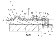
以下、サーマルヘッドX1について図1〜5を参照して説明する。図1においては、保護層25、被覆層27、および被覆部材12を省略して一点鎖線にて示している。なお、図5(a)においては、被覆部材12の図示を省略しており、図7(a),7(b),8(a),9(a),9(b),10においても同様である。
<First Embodiment>
Hereinafter, the thermal head X1 will be described with reference to FIGS. In FIG. 1, the protective layer 25, the covering layer 27, and the covering member 12 are omitted and indicated by a one-dot chain line. 5A, illustration of the covering member 12 is omitted, and also in FIGS. 7A, 7B, 8A, 9A, 9B, and 10. It is the same.

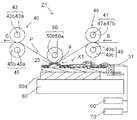
サーマルヘッドX1は、放熱体1と、放熱体1上に配置されたヘッド基体3と、ヘッド基体3に接続されたコネクタ31とを備えている。   The thermal head X <b> 1 includes a heat radiator 1, a head base 3 disposed on the heat sink 1, and a connector 31 connected to the head base 3.

放熱体1は、直方体形状をなしており、基板7が載置される台部1aを有している。放熱体1の上方には基板7とコネクタ31のハウジング10が配置されている。   The heat radiating body 1 has a rectangular parallelepiped shape and includes a base 1a on which the substrate 7 is placed. A substrate 10 and a housing 10 for a connector 31 are disposed above the radiator 1.

放熱体1は、例えば、銅、鉄またはアルミニウム等の金属材料で形成されており、ヘッド基体3の発熱部9で発生した熱のうち、印画に寄与しない熱を放熱する機能を有している。また、台部1aの上面には、両面テープあるいは接着剤等(不図示)によってヘッド基体3が接着されている。   The radiator 1 is formed of a metal material such as copper, iron, or aluminum, for example, and has a function of radiating heat that does not contribute to printing out of heat generated in the heat generating portion 9 of the head base 3. . Further, the head base 3 is bonded to the upper surface of the base portion 1a by a double-sided tape or an adhesive (not shown).

ヘッド基体3は、平面視して、長方形状に形成されており、ヘッド基体3の基板7上にサーマルヘッドX1を構成する各部材が設けられている。ヘッド基体3は、外部より供給された電気信号に従い、記録媒体(不図示)に印字を行う機能を有する。   The head base 3 is formed in a rectangular shape in plan view, and each member constituting the thermal head X1 is provided on the substrate 7 of the head base 3. The head base 3 has a function of printing on a recording medium (not shown) in accordance with an electric signal supplied from the outside.

コネクタ31は、図2に示すように、複数のコネクタピン8と、複数のコネクタピン8を収納するハウジング10とを有している。複数のコネクタピン8は、一方がハウジング10の外部に露出しており、他方がハウジング10の内部に収容されている。複数のコネクタピン8は、ヘッド基体3の各種電極と、外部に設けられた例えば電源との電気的な導通を確保する機能を有しており、それぞれが電気的に独立している。   As illustrated in FIG. 2, the connector 31 includes a plurality of connector pins 8 and a housing 10 that houses the plurality of connector pins 8. One of the plurality of connector pins 8 is exposed to the outside of the housing 10, and the other is accommodated inside the housing 10. The plurality of connector pins 8 have a function of ensuring electrical continuity between various electrodes of the head base 3 and, for example, a power source provided outside, and each is electrically independent.

以下、ヘッド基体3を構成する各部材について説明する。   Hereinafter, each member constituting the head base 3 will be described.

基板7は、放熱体1の台部1a上に配置されており、平面視して、矩形状をなしている。そのため、基板7は、一方の長辺7aと、他方の長辺7bと、一方の短辺7cと、他方の短辺7dとを有している。また、他方の短辺7b側に側面7eを有している。基板7は、例えば、アルミナセラミックス等の電気絶縁性材料あるいは単結晶シリコン等の半導体材料等によって形成されている。   The board | substrate 7 is arrange | positioned on the base part 1a of the heat radiator 1, and has comprised the rectangular shape by planar view. Therefore, the substrate 7 has one long side 7a, the other long side 7b, one short side 7c, and the other short side 7d. Moreover, it has the side surface 7e in the other short side 7b side. The substrate 7 is formed of, for example, an electrically insulating material such as alumina ceramic or a semiconductor material such as single crystal silicon.

基板7の上面には、蓄熱層13が形成されている。蓄熱層13は、基板7の上面の左半分にわたり形成された下地部13aと、複数の発熱部9の配列方向に沿って帯状に延び、
断面が略半楕円形状をなしている隆起部13bとを有している。下地部13aは、発熱部9の近傍に設けられており、後述する保護層25の下方に配置されている。隆起部13bは、印画する記録媒体を、発熱部9上に形成された保護層25に良好に押し当てるように機能する。
A heat storage layer 13 is formed on the upper surface of the substrate 7. The heat storage layer 13 extends in a strip shape along the arrangement direction of the base portion 13a formed over the left half of the upper surface of the substrate 7 and the plurality of heat generating portions 9,
And a raised portion 13b having a substantially semi-elliptical cross section. The base portion 13a is provided in the vicinity of the heat generating portion 9, and is disposed below a protective layer 25 described later. The raised portion 13b functions to favorably press the recording medium to be printed against the protective layer 25 formed on the heat generating portion 9.

蓄熱層13は、熱伝導性の低いガラスで形成されており、発熱部9で発生する熱の一部を一時的に蓄積することで、発熱部9の温度を上昇させるのに要する時間を短くすることができ、サーマルヘッドX1の熱応答特性を高めるように機能する。蓄熱層13は、例えば、ガラス粉末に適当な有機溶剤を混合して得た所定のガラスペーストを従来周知のスクリーン印刷等によって基板7の上面に塗布し、これを焼成することで形成される。   The heat storage layer 13 is formed of glass having low thermal conductivity, and by temporarily storing a part of the heat generated in the heat generating part 9, the time required to raise the temperature of the heat generating part 9 is shortened. And functions to enhance the thermal response characteristics of the thermal head X1. The heat storage layer 13 is formed, for example, by applying a predetermined glass paste obtained by mixing a glass powder with an appropriate organic solvent onto the upper surface of the substrate 7 by screen printing or the like known in the art, and baking it.

電気抵抗層15は、蓄熱層13の上面に設けられており、電気抵抗層15上には、接続端子2、グランド電極4、共通電極17、個別電極19、IC−コネクタ接続電極21、およびIC−IC接続電極26が設けられている。電気抵抗層15は、接続端子2、グランド電極4、共通電極17、個別電極19、IC−コネクタ接続電極21、およびIC−IC接続電極26と同形状にパターニングされており、共通電極17と個別電極19との間に電気抵抗層15が露出した露出領域を有する。電気抵抗層15の露出領域は、図1に示すように、蓄熱層13の隆起部13b上に列状に配置されており、各露出領域が発熱部9を構成している。   The electrical resistance layer 15 is provided on the upper surface of the heat storage layer 13. On the electrical resistance layer 15, the connection terminal 2, the ground electrode 4, the common electrode 17, the individual electrode 19, the IC-connector connection electrode 21, and the IC -An IC connection electrode 26 is provided. The electrical resistance layer 15 is patterned in the same shape as the connection terminal 2, the ground electrode 4, the common electrode 17, the individual electrode 19, the IC-connector connection electrode 21, and the IC-IC connection electrode 26. Between the electrode 19, there is an exposed region where the electric resistance layer 15 is exposed. As shown in FIG. 1, the exposed regions of the electrical resistance layer 15 are arranged in a row on the raised portions 13 b of the heat storage layer 13, and each exposed region constitutes the heat generating portion 9.

複数の発熱部9は、説明の便宜上、図1では簡略化して記載しているが、例えば、100dpi〜2400dpi(dot per inch)等の密度で配置される。電気抵抗層15は、例えば、TaN系、TaSiO系、TaSiNO系、TiSiO系、TiSiCO系またはNbSiO系等の電気抵抗の比較的高い材料によって形成されている。そのため、発熱部9に電圧が印加されたときに、ジュール発熱によって発熱部9が発熱する。   For convenience of explanation, the plurality of heat generating portions 9 are illustrated in a simplified manner in FIG. 1, but are arranged at a density of, for example, 100 dpi to 2400 dpi (dot per inch). The electric resistance layer 15 is made of a material having a relatively high electric resistance, such as TaN, TaSiO, TaSiNO, TiSiO, TiSiCO, or NbSiO. Therefore, when a voltage is applied to the heat generating portion 9, the heat generating portion 9 generates heat due to Joule heat generation.

図1,2に示すように、電気抵抗層15の上面には、接続端子2、グランド電極4、共通電極17、複数の個別電極19、IC−コネクタ接続電極21、およびIC−IC接続電極26が設けられている。これらの接続端子2、グランド電極4、共通電極17、個別電極19、IC−コネクタ接続電極21、およびIC−IC接続電極26は、導電性を有する材料で形成されており、例えば、アルミニウム、金、銀および銅のうちのいずれか一種の金属またはこれらの合金によって形成されている。   As shown in FIGS. 1 and 2, the connection terminal 2, the ground electrode 4, the common electrode 17, the plurality of individual electrodes 19, the IC-connector connection electrode 21, and the IC-IC connection electrode 26 are provided on the upper surface of the electrical resistance layer 15. Is provided. The connection terminal 2, the ground electrode 4, the common electrode 17, the individual electrode 19, the IC-connector connection electrode 21, and the IC-IC connection electrode 26 are made of a conductive material. For example, aluminum, gold , Any one of silver and copper, or an alloy thereof.

共通電極17は、主配線部17a,17dと、副配線部17bと、リード部17cとを備えている。主配線部17aは、基板7の一方の長辺に沿って延びている。副配線部17bは、基板7の一方および他方の短辺のそれぞれに沿って延びている。リード部17cは、主配線部17aから各発熱部9に向かって個別に延びている。主配線部17dは、基板7の他方の長辺に沿って延びている。   The common electrode 17 includes main wiring portions 17a and 17d, a sub wiring portion 17b, and a lead portion 17c. The main wiring portion 17 a extends along one long side of the substrate 7. The sub wiring part 17 b extends along one and the other short sides of the substrate 7. The lead portion 17c extends individually from the main wiring portion 17a toward each heat generating portion 9. The main wiring portion 17 d extends along the other long side of the substrate 7.

共通電極17は、複数の発熱部9と、コネクタ31とを電気的に接続している。なお、主配線部17aの電気抵抗値を低下させるために、主配線部17aを他の共通電極17の部位より厚い厚電極部(不図示)としてもよい。   The common electrode 17 electrically connects the plurality of heat generating portions 9 and the connector 31. In addition, in order to reduce the electrical resistance value of the main wiring part 17a, the main wiring part 17a may be a thick electrode part (not shown) thicker than other parts of the common electrode 17.

複数の個別電極19は、発熱部9と駆動IC11との間を電気的に接続している。また、個別電極19は、複数の発熱部9を複数の群に分けており、各群の発熱部9と各群に対応して設けられた駆動IC11とを電気的に接続している。   The plurality of individual electrodes 19 are electrically connected between the heat generating portion 9 and the drive IC 11. In addition, the individual electrode 19 divides the plurality of heat generating portions 9 into a plurality of groups, and electrically connects the heat generating portions 9 of each group and the drive IC 11 provided corresponding to each group.

複数のIC−コネクタ接続電極21は、駆動IC11とコネクタ31との間を電気的に接続している。各駆動IC11に接続された複数のIC−コネクタ接続電極21は、異なる機能を有する複数の配線で構成されている。   The plurality of IC-connector connection electrodes 21 electrically connect the drive IC 11 and the connector 31. The plurality of IC-connector connection electrodes 21 connected to each drive IC 11 are composed of a plurality of wirings having different functions.

グランド電極4は、個別電極19と、IC−コネクタ接続電極21と、共通電極17の主配線部17dとにより取り囲むように配置されており、広い面積を有している。グランド電極4は、0〜1Vのグランド電位に保持されている。   The ground electrode 4 is disposed so as to be surrounded by the individual electrode 19, the IC-connector connection electrode 21, and the main wiring portion 17 d of the common electrode 17, and has a wide area. The ground electrode 4 is held at a ground potential of 0 to 1V.

接続端子2は、共通電極17、個別電極19、IC−コネクタ接続電極21およびグランド電極4をコネクタ31に接続するために、基板7の他方の長辺7b側に設けられている。接続端子2はコネクタピン8に対応して設けられており、コネクタ31に接続する際は、それぞれ電気的に独立するようにコネクタピン8と接続端子2とが接続されている。   The connection terminal 2 is provided on the other long side 7 b side of the substrate 7 in order to connect the common electrode 17, the individual electrode 19, the IC-connector connection electrode 21, and the ground electrode 4 to the connector 31. The connection terminal 2 is provided corresponding to the connector pin 8, and when connecting to the connector 31, the connector pin 8 and the connection terminal 2 are connected so as to be electrically independent from each other.

複数のIC−IC接続電極26は、隣り合う駆動IC11を電気的に接続している。複数のIC−IC接続電極26は、それぞれIC−コネクタ接続電極21に対応するように設けられており、各種信号を隣り合う駆動IC11に伝えている。   The plurality of IC-IC connection electrodes 26 electrically connect adjacent drive ICs 11. The plurality of IC-IC connection electrodes 26 are provided so as to correspond to the IC-connector connection electrodes 21, respectively, and transmit various signals to the adjacent drive ICs 11.

上記の電気抵抗層15、接続端子2、共通電極17、個別電極19、グランド電極4、IC−コネクタ接続電極21、およびIC−IC接続電極26は、例えば、各々を構成する材料層を蓄熱層13上に、例えばスパッタリング法等の従来周知の薄膜成形技術によって順次積層した後、積層体を従来周知のフォトエッチング等を用いて所定のパターンに加工することにより形成される。なお、接続端子2、共通電極17、個別電極19、グランド電極4、IC−コネクタ接続電極21、およびIC−IC接続電極26は、同じ工程によって同時に形成することができる。   The electrical resistance layer 15, the connection terminal 2, the common electrode 17, the individual electrode 19, the ground electrode 4, the IC-connector connection electrode 21, and the IC-IC connection electrode 26 are, for example, a material layer constituting each of the heat storage layers. 13 is formed by sequentially laminating the film 13 by a conventionally well-known thin film forming technique such as a sputtering method, and then processing the laminated body into a predetermined pattern using a conventionally well-known photoetching or the like. The connection terminal 2, the common electrode 17, the individual electrode 19, the ground electrode 4, the IC-connector connection electrode 21, and the IC-IC connection electrode 26 can be formed simultaneously by the same process.

駆動IC11は、図1に示すように、複数の発熱部9の各群に対応して配置されているとともに、個別電極19の他端部とIC−コネクタ接続電極21の一端部とに接続されている。駆動IC11は、各発熱部9の通電状態を制御する機能を有している。駆動IC11としては、内部に複数のスイッチング素子を有する切替部材を用いればよい。   As shown in FIG. 1, the driving IC 11 is disposed corresponding to each group of the plurality of heat generating units 9 and is connected to the other end of the individual electrode 19 and one end of the IC-connector connection electrode 21. ing. The drive IC 11 has a function of controlling the energization state of each heat generating unit 9. As the drive IC 11, a switching member having a plurality of switching elements inside may be used.

駆動IC11は、個別電極19、IC−IC接続電極26およびIC−コネクタ接続電極21に接続された状態で、駆動IC11の保護、および駆動IC11とこれらの配線との接続部の保護のため、エポキシ樹脂、あるいはシリコーン樹脂等の樹脂からなるハードコート29によって封止されている。   The drive IC 11 is connected to the individual electrode 19, the IC-IC connection electrode 26 and the IC-connector connection electrode 21 in order to protect the drive IC 11 and to protect the connection portion between the drive IC 11 and these wirings. It is sealed with a hard coat 29 made of a resin or a resin such as a silicone resin.

図1,2に示すように、基板7の上面に形成された蓄熱層13上には、発熱部9、共通電極17の一部および個別電極19の一部を被覆する保護層25が形成されている。   As shown in FIGS. 1 and 2, a protective layer 25 is formed on the heat storage layer 13 formed on the upper surface of the substrate 7 to cover the heat generating portion 9, a part of the common electrode 17 and a part of the individual electrode 19. ing.

保護層25は、発熱部9、共通電極17および個別電極19の被覆した領域を、大気中に含まれている水分等の付着による腐食、あるいは印画する記録媒体との接触による摩耗から保護するためのものである。保護層25は、SiN、SiO、SiON、SiC、あるいはダイヤモンドライクカーボン等を用いて形成することができ、保護層25を単層で構成してもよいし、これらの層を積層して構成してもよい。このような保護層25はスパッタリング法等の薄膜形成技術あるいはスクリーン印刷等の厚膜形成技術を用いて作製することができる。 The protective layer 25 protects the area covered with the heat generating portion 9, the common electrode 17 and the individual electrode 19 from corrosion due to adhesion of moisture or the like contained in the atmosphere, or wear due to contact with the recording medium to be printed. belongs to. The protective layer 25 can be formed using SiN, SiO 2 , SiON, SiC, diamond-like carbon, or the like, and the protective layer 25 may be formed of a single layer or may be formed by stacking these layers. May be. Such a protective layer 25 can be produced using a thin film forming technique such as sputtering or a thick film forming technique such as screen printing.

また、図1,2に示すように、基板7上には、共通電極17、個別電極19およびIC−コネクタ接続電極21を部分的に被覆する被覆部材27が設けられている。なお、図1では、説明の便宜上、被覆部材27の形成領域を一点鎖線で示している。被覆部材27は、共通電極17、個別電極19、IC−IC接続電極26およびIC−コネクタ接続電極21の被覆した領域を、大気との接触による酸化、あるいは大気中に含まれている水分等の付着による腐食から保護するためのものである。   As shown in FIGS. 1 and 2, a covering member 27 that partially covers the common electrode 17, the individual electrode 19, and the IC-connector connection electrode 21 is provided on the substrate 7. In FIG. 1, for convenience of explanation, the formation region of the covering member 27 is indicated by a one-dot chain line. The covering member 27 oxidizes the region covered with the common electrode 17, the individual electrode 19, the IC-IC connection electrode 26 and the IC-connector connection electrode 21 by contact with the atmosphere, or moisture contained in the atmosphere. It is intended to protect against corrosion due to adhesion.

なお、被覆部材27は、共通電極17および個別電極19の保護をより確実にするため、図2に示すように保護層25の端部に重なるようにして形成されることが好ましい。被覆部材27は、例えば、エポキシ樹脂、あるいはポリイミド樹脂等の樹脂材料をスクリーン印刷法等の厚膜成形技術を用いて形成することができる。   The covering member 27 is preferably formed so as to overlap the end portion of the protective layer 25 as shown in FIG. 2 in order to ensure the protection of the common electrode 17 and the individual electrode 19. The covering member 27 can be formed of a resin material such as an epoxy resin or a polyimide resin by using a thick film forming technique such as a screen printing method.

被覆部材27は、駆動IC11と接続される個別電極19、IC−IC接続電極26およびIC−コネクタ接続電極21を露出させるための開口部27aが形成されている。そして、開口部27aから露出したこれらの配線が駆動IC11に接続されている。また、被覆部材27は、基板7の他方の長辺7b側に、接続端子2を露出させるための開口部27bが設けられている。開口部27bから露出した接続端子2は、コネクタピン8と電気的に接続される。   The covering member 27 is formed with an opening 27 a for exposing the individual electrode 19, the IC-IC connection electrode 26, and the IC-connector connection electrode 21 connected to the driving IC 11. These wirings exposed from the opening 27a are connected to the driving IC 11. The covering member 27 is provided with an opening 27 b for exposing the connection terminal 2 on the other long side 7 b side of the substrate 7. The connection terminal 2 exposed from the opening 27b is electrically connected to the connector pin 8.

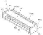
図3〜5を用いて、コネクタ31およびコネクタ31とヘッド基体3との接合について詳細に説明する。図4(a),5(a)については、被覆部材12を省略して示している。   The connection between the connector 31 and the connector 31 and the head base 3 will be described in detail with reference to FIGS. 4 (a) and 5 (a), the covering member 12 is omitted.

コネクタ31は、複数のコネクタピン8と、複数のコネクタピン8を収容するハウジング10とを備えている。   The connector 31 includes a plurality of connector pins 8 and a housing 10 that houses the plurality of connector pins 8.

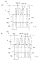
図4に示すように、コネクタピン8は、上部コネクタピン8aと、下部コネクタピン8bと、連結部8cと、引き出し部8dとを備えている。コネクタピン8は、主走査方向に間隔をあけて複数配列されている。コネクタピン8同士は、互いに離間しており、隣り合うコネクタピン8は、電気的に絶縁されている。   As shown in FIG. 4, the connector pin 8 includes an upper connector pin 8a, a lower connector pin 8b, a connecting portion 8c, and a drawer portion 8d. A plurality of connector pins 8 are arranged at intervals in the main scanning direction. The connector pins 8 are separated from each other, and the adjacent connector pins 8 are electrically insulated.

上部コネクタピン8aは、接続端子2(図1参照)上に配置されている。下部コネクタピン8bは、ヘッド基体3の基板7の下方に配置されている。そして、上部コネクタピン8aと下部コネクタピン8bとにより、ヘッド基体3を挟持している。連結部8cは、上部コネクタピン8aと下部コネクタピン8bとを連結しており、厚み方向に延びるように設けられている。引き出し部8dは、ヘッド基体3から離れる方向に引き出されており、下部コネクタピン8bから連続的に設けられている。   The upper connector pin 8a is disposed on the connection terminal 2 (see FIG. 1). The lower connector pin 8 b is disposed below the substrate 7 of the head base 3. The head base 3 is sandwiched between the upper connector pin 8a and the lower connector pin 8b. The connecting portion 8c connects the upper connector pin 8a and the lower connector pin 8b, and is provided so as to extend in the thickness direction. The lead portion 8d is drawn away from the head base 3, and is continuously provided from the lower connector pin 8b.

コネクタピン8は、上部コネクタピン8aと、下部コネクタピン8bと、連結部8cと、引き出し部8dとが一体的に設けられており、上部コネクタピン8aと、下部コネクタピン8bとにより形成された空間に、ヘッド基体3が挿入されることにより、コネクタ31とヘッド基体3とが連結されている。   The connector pin 8 includes an upper connector pin 8a, a lower connector pin 8b, a connecting portion 8c, and a drawer portion 8d, and is formed by the upper connector pin 8a and the lower connector pin 8b. By inserting the head base 3 into the space, the connector 31 and the head base 3 are connected.

ハウジング10は、各コネクタピン8をそれぞれ電気的に独立された状態で収納する機能を有する。外部に設けられたケーブル(不図示)等の着脱により、ヘッド基体3に電気を供給している。   The housing 10 has a function of housing each connector pin 8 in an electrically independent state. Electricity is supplied to the head base 3 by attaching and detaching a cable (not shown) provided outside.

ハウジング10は、上壁10aと、下壁10bと、側壁10cと、前壁10dと、突出部10eと、位置決め部10fとを備えている。ハウジング10は、上壁10aと、下壁10bと、側壁10cと、前壁10dとにより、全体として、コネクタピン8の引き出し部8d側が開口した箱形状をなしている。   The housing 10 includes an upper wall 10a, a lower wall 10b, a side wall 10c, a front wall 10d, a protruding portion 10e, and a positioning portion 10f. The housing 10 has a box shape in which the lead portion 8d side of the connector pin 8 is opened as a whole by the upper wall 10a, the lower wall 10b, the side wall 10c, and the front wall 10d.

突出部10eは、平面視して、上壁10aから隣り合う上部コネクタピン8a同士の間に向けて突出しており、ヘッド基体3側に向けて延びている。いる。また、主走査方向の両端に位置する突出部10eは、位置決め部10fと上部コネクタピン8aとの間に向けて突出しており、ヘッド基体3側に向けて延びている。   The protrusion 10e protrudes from the upper wall 10a toward the adjacent upper connector pins 8a in plan view, and extends toward the head base 3 side. Yes. In addition, the protruding portions 10e located at both ends in the main scanning direction protrude between the positioning portion 10f and the upper connector pin 8a, and extend toward the head base 3 side.

コネクタピン8は、導電性を有する必要があるため、金属あるいは合金により形成することができる。ハウジング10は、絶縁性の部材により形成することができ、例えば、PA(ポリアミド)、PBT(ポリブチレンテレフタレート)、LCP(液晶ポリマー)、ナイロン66、ガラス入りナイロン66などの樹脂により形成することができる。   Since the connector pin 8 needs to have conductivity, it can be formed of a metal or an alloy. The housing 10 can be formed of an insulating member. For example, the housing 10 can be formed of a resin such as PA (polyamide), PBT (polybutylene terephthalate), LCP (liquid crystal polymer), nylon 66, and glass-filled nylon 66. it can.

図1,2,4(b),5(b)に示すように、コネクタ31とヘッド基体3とは、コネクタピン8、導電性接合材23、および被覆部材12により固定されている。   As shown in FIGS. 1, 2, 4 (b), and 5 (b), the connector 31 and the head base 3 are fixed by the connector pins 8, the conductive bonding material 23, and the covering member 12.

図1,2に示すように、グランド電極4の接続端子2およびIC−コネクタ接続電極21の接続端子2上には、コネクタピン8が配置されている。図2に示すように、接続端子2と、コネクタピン8とは、導電性接合材23により電気的に接続されている。   As shown in FIGS. 1 and 2, connector pins 8 are arranged on the connection terminal 2 of the ground electrode 4 and the connection terminal 2 of the IC-connector connection electrode 21. As shown in FIG. 2, the connection terminal 2 and the connector pin 8 are electrically connected by a conductive bonding material 23.

導電性接合材23は、例えば、はんだ、あるいは電気絶縁性の樹脂中に導電性粒子が混入された異方性導電接着剤等を例示することができる。本実施形態においては、はんだを用いて説明する。コネクタピン8は、導電性接合材23に覆われることにより、接続端子2と電気的に接続されている。なお、導電性接合材23と接続端子2との間にNi、Au、あるいはPdによるめっき層(不図示)を設けてもよい。   Examples of the conductive bonding material 23 include solder or an anisotropic conductive adhesive in which conductive particles are mixed in an electrically insulating resin. In the present embodiment, description will be made using solder. The connector pin 8 is electrically connected to the connection terminal 2 by being covered with the conductive bonding material 23. A plating layer (not shown) of Ni, Au, or Pd may be provided between the conductive bonding material 23 and the connection terminal 2.

被覆部材12は、上部コネクタピン8a、ハウジング10の上壁10a、およびヘッド基体3の上面に配置されている。被覆部材12は、例えば、エポキシ系の熱硬化性の樹脂、紫外線硬化性の樹脂、あるいは可視光硬化性の樹脂により形成することができる。   The covering member 12 is disposed on the upper connector pin 8 a, the upper wall 10 a of the housing 10, and the upper surface of the head base 3. The covering member 12 can be formed of, for example, an epoxy thermosetting resin, an ultraviolet curable resin, or a visible light curable resin.

被覆部材12を熱硬化性の樹脂により形成した場合、サーマルヘッドX1は、ヘッド基体3を上部コネクタピン8aと下部コネクタピン8bとの間に挿入し、コネクタピン8と、ヘッド基体3とを導電性接合材23により接続した後に、両面テープ等が設けられた放熱体1上に、ヘッド基体3を載置する。そして、上部コネクタピン8aを封止するように、被覆部材12を塗布、硬化することにより、作製することができる。   When the covering member 12 is formed of a thermosetting resin, the thermal head X1 inserts the head base 3 between the upper connector pin 8a and the lower connector pin 8b, and conducts the connector pin 8 and the head base 3 electrically. After connecting with the conductive bonding material 23, the head substrate 3 is placed on the radiator 1 provided with a double-sided tape or the like. And it can produce by apply | coating and hardening the coating | coated member 12 so that the upper connector pin 8a may be sealed.

サーマルヘッドX1は、ハウジング10が、平面視して、隣り合う上部コネクタピン8a同士の間に向けて突出する突出部10fを有する構成である。これにより、コネクタピン8を被覆部材12にて封止するために被覆部材12を塗布した場合に、突出部10fにより、被覆部材12が下方へ流出することを低減することができる。   The thermal head X1 has a configuration in which the housing 10 has a protruding portion 10f that protrudes between adjacent upper connector pins 8a in plan view. Thereby, when the coating member 12 is applied in order to seal the connector pin 8 with the coating member 12, it is possible to reduce the downward flow of the coating member 12 by the protruding portion 10f.

すなわち、突出部10fが被覆部材12を堰き止めることにより、被覆部材12をハウジング10の上部に留まらせることができる。その結果、ハウジング10の上部にて被覆部材12が不足する可能性を低減することができ、コネクタピン8を封止することができる。   In other words, the covering member 12 can be kept on the upper portion of the housing 10 by the projecting portion 10 f blocking the covering member 12. As a result, the possibility that the covering member 12 is insufficient at the upper part of the housing 10 can be reduced, and the connector pin 8 can be sealed.

また、サーマルヘッドX1は、被覆部材12をハウジング10の上部に留まらせることができるため、コネクタピン8とヘッド基体3とを強固に固定することができる。それにより、コネクタ31とヘッド基体3との接合強度を強固なものとすることができる。   Further, since the thermal head X1 can keep the covering member 12 on the upper portion of the housing 10, the connector pin 8 and the head base 3 can be firmly fixed. Thereby, the joining strength between the connector 31 and the head base 3 can be strengthened.

特に、図4(a)に示すように、平面視して、隣り合う上部コネクタピン8a同士の間の長さと、突出部10eの幅が等しいことが好ましい。このような場合、被覆部材12の下方への流出をさらに抑えることができる。   In particular, as shown in FIG. 4A, it is preferable that the length between the adjacent upper connector pins 8a and the width of the protruding portion 10e are equal in plan view. In such a case, the downward flow of the covering member 12 can be further suppressed.

図5(a)に示すように、突出部10eの突出長さLeが、位置決め部10fの突出長さLfと略等しいことが好ましい。それにより、ヘッド基体3と、突出部10eとの間に隙間が生じにくくなり、被覆部材12が下方に流出する可能性をさらに低減することができる。なお、突出部10eの突出長さLeと、位置決め部10fの突出長さLfとが略等
しいとは、突出部10eの突出長さLeと、位置決め部10fの突出長さLfとの差が、突出部10eの突出長さLeおよび位置決め部10fの突出長さLfの±10%程度の製造誤差を含む概念である。
As shown in FIG. 5A, it is preferable that the protruding length Le of the protruding portion 10e is substantially equal to the protruding length Lf of the positioning portion 10f. This makes it difficult for a gap to be formed between the head base 3 and the protruding portion 10e, and the possibility of the covering member 12 flowing out downward can be further reduced. Note that the protrusion length Le of the protrusion 10e and the protrusion length Lf of the positioning portion 10f are substantially equal means that the difference between the protrusion length Le of the protrusion 10e and the protrusion length Lf of the positioning portion 10f is This is a concept including a manufacturing error of about ± 10% of the protruding length Le of the protruding portion 10e and the protruding length Lf of the positioning portion 10f.

図5(b)に示すように、上部コネクタピン8aの下面8eは、突出部10eの上面10gよりも高く配置されている。そのため、突出部10eと、上部コネクタピン8aとの間に隙間14が生じることとなる。それにより、コネクタピン8に塗布した被覆部材12の一部が、隙間14を通り、上部コネクタピン8aの下面8eにまで回り込むこととなる。   As shown in FIG. 5B, the lower surface 8e of the upper connector pin 8a is arranged higher than the upper surface 10g of the protruding portion 10e. Therefore, a gap 14 is generated between the protruding portion 10e and the upper connector pin 8a. Thereby, a part of the covering member 12 applied to the connector pin 8 passes through the gap 14 and reaches the lower surface 8e of the upper connector pin 8a.

それにより、被覆部材12が、上部コネクタピン8aの全面を取り囲むように配置されることとなり、コネクタピン8aの封止性を向上させることができる。   Thereby, the covering member 12 is disposed so as to surround the entire surface of the upper connector pin 8a, and the sealing performance of the connector pin 8a can be improved.

次に、サーマルプリンタZ1について、図6を参照しつつ説明する。   Next, the thermal printer Z1 will be described with reference to FIG.

図6に示すように、本実施形態のサーマルプリンタZ1は、上述のサーマルヘッドX1と、搬送機構40と、プラテンローラ50と、電源装置60と、制御装置70とを備えている。サーマルヘッドX1は、サーマルプリンタZ1の筐体(不図示)に設けられた取付部材80の取付面80aに取り付けられている。なお、サーマルヘッドX1は、後述する記録媒体Pの搬送方向Sに直交する方向である主走査方向に沿うようにして、取付部材80に取り付けられている。   As shown in FIG. 6, the thermal printer Z <b> 1 of the present embodiment includes the above-described thermal head X <b> 1, a transport mechanism 40, a platen roller 50, a power supply device 60, and a control device 70. The thermal head X1 is attached to an attachment surface 80a of an attachment member 80 provided in a housing (not shown) of the thermal printer Z1. The thermal head X1 is attached to the attachment member 80 so as to be along a main scanning direction which is a direction orthogonal to the conveyance direction S of the recording medium P described later.

搬送機構40は、駆動部(不図示)と、搬送ローラ43,45,47,49とを有している。搬送機構40は、感熱紙、インクが転写される受像紙等の記録媒体Pを図6の矢印S方向に搬送して、サーマルヘッドX1の複数の発熱部9上に位置する保護層25上に搬送するためのものである。駆動部は、搬送ローラ43,45,47,49を駆動させる機能を有しており、例えば、モータを用いることができる。搬送ローラ43,45,47,49は、例えば、ステンレス等の金属からなる円柱状の軸体43a,45a,47a,49aを、ブタジエンゴム等からなる弾性部材43b,45b,47b,49bにより被覆して構成することができる。なお、図示しないが、記録媒体Pがインクが転写される受像紙等の場合は、記録媒体PとサーマルヘッドX1の発熱部9との間に、記録媒体Pとともにインクフィルムを搬送する。   The transport mechanism 40 includes a drive unit (not shown) and transport rollers 43, 45, 47, and 49. The transport mechanism 40 transports a recording medium P such as thermal paper or image receiving paper onto which ink is transferred in the direction of arrow S in FIG. 6 and then onto the protective layer 25 positioned on the plurality of heat generating portions 9 of the thermal head X1. It is for carrying. The drive unit has a function of driving the transport rollers 43, 45, 47, and 49, and for example, a motor can be used. The transport rollers 43, 45, 47, and 49 are formed by, for example, covering cylindrical shaft bodies 43a, 45a, 47a, and 49a made of metal such as stainless steel with elastic members 43b, 45b, 47b, and 49b made of butadiene rubber or the like. Can be configured. Although not shown, when the recording medium P is an image receiving paper or the like to which ink is transferred, an ink film is transported together with the recording medium P between the recording medium P and the heat generating portion 9 of the thermal head X1.

プラテンローラ50は、記録媒体PをサーマルヘッドX1の発熱部9上に位置する保護膜25上に押圧する機能を有する。プラテンローラ50は、記録媒体Pの搬送方向Sに直交する方向に沿って延びるように配置され、記録媒体Pを発熱部9上に押圧した状態で回転可能となるように両端部が支持固定されている。プラテンローラ50は、例えば、ステンレス等の金属からなる円柱状の軸体50aを、ブタジエンゴム等からなる弾性部材50bにより被覆して構成することができる。   The platen roller 50 has a function of pressing the recording medium P onto the protective film 25 located on the heat generating portion 9 of the thermal head X1. The platen roller 50 is disposed so as to extend along a direction orthogonal to the conveyance direction S of the recording medium P, and both ends thereof are supported and fixed so as to be rotatable while the recording medium P is pressed onto the heat generating portion 9. ing. The platen roller 50 can be configured by, for example, covering a cylindrical shaft body 50a made of metal such as stainless steel with an elastic member 50b made of butadiene rubber or the like.

電源装置60は、上記のようにサーマルヘッドX1の発熱部9を発熱させるための電流および駆動IC11を動作させるための電流を供給する機能を有している。制御装置70は、上記のようにサーマルヘッドX1の発熱部9を選択的に発熱させるために、駆動IC11の動作を制御する制御信号を駆動IC11に供給する機能を有している。   The power supply device 60 has a function of supplying a current for generating heat from the heat generating portion 9 of the thermal head X1 and a current for operating the drive IC 11 as described above. The control device 70 has a function of supplying a control signal for controlling the operation of the drive IC 11 to the drive IC 11 in order to selectively heat the heat generating portion 9 of the thermal head X1 as described above.

サーマルプリンタZ1は、図6に示すように、プラテンローラ50によって記録媒体PをサーマルヘッドX1の発熱部9上に押圧しつつ、搬送機構40によって記録媒体Pを発熱部9上に搬送しながら、電源装置60および制御装置70によって発熱部9を選択的に発熱させることにより、記録媒体Pに所定の印画を行う。なお、記録媒体Pが受像紙等の場合は、記録媒体Pとともに搬送されるインクフィルム(不図示)のインクを記録媒体P
に熱転写することによって、記録媒体Pへの印画を行う。
As shown in FIG. 6, the thermal printer Z1 presses the recording medium P onto the heat generating part 9 of the thermal head X1 by the platen roller 50, and conveys the recording medium P onto the heat generating part 9 by the conveying mechanism 40. The heat generating unit 9 is selectively heated by the power supply device 60 and the control device 70 to perform predetermined printing on the recording medium P. When the recording medium P is image receiving paper or the like, the ink of an ink film (not shown) conveyed with the recording medium P is used as the recording medium P.
Is printed on the recording medium P.

<第2の実施形態>
図7を用いてサーマルヘッドX2について説明する。なお、サーマルヘッドX1と同一の部材については同一の符号を付し、以下同様とする。
<Second Embodiment>
The thermal head X2 will be described with reference to FIG. The same members as those of the thermal head X1 are denoted by the same reference numerals, and so on.

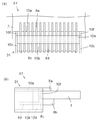
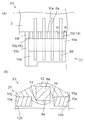
図7(a)に示すように、サーマルヘッドX2は、突出部10eに切欠部10iが設けられており、切欠部10iには、被覆部材12(図1参照)が配置されている。切欠部10iは、突出部10eのヘッド基体3側の角部を取り除くように設けられており、1つの突出部10eに対して2つ設けられている。そして、突出部10eは、主走査方向における中央部にてヘッド基体3と接触しており、平面視して、突出部10eと、ヘッド基体3と、上部コネクタピン8aとにより囲まれた隙間16に、被覆部材12が充填されている。   As shown in FIG. 7A, the thermal head X2 is provided with a notch 10i in the protrusion 10e, and a covering member 12 (see FIG. 1) is arranged in the notch 10i. The notches 10i are provided so as to remove the corners on the head base 3 side of the protrusion 10e, and two notches 10i are provided for one protrusion 10e. The protrusion 10e is in contact with the head base 3 at the center in the main scanning direction, and in a plan view, the gap 16 surrounded by the protrusion 10e, the head base 3, and the upper connector pin 8a. Further, the covering member 12 is filled.

サーマルヘッドX2は、突出部10eに切欠部10iが設けられており、切欠部10iによって形成された隙間16に被覆部材12が充填されている。そのため、突出部10eと、ヘッド基体3と、上部コネクタピン8aとの接合強度を向上させることができる。その結果、ヘッド基体3とコネクタ31との接合強度を向上させることができる。   The thermal head X2 is provided with a notch 10i in the protruding portion 10e, and the covering member 12 is filled in the gap 16 formed by the notch 10i. Therefore, it is possible to improve the bonding strength between the protruding portion 10e, the head base 3, and the upper connector pin 8a. As a result, the bonding strength between the head base 3 and the connector 31 can be improved.

また、平面視して、切欠部10iは、突出部10eのうち、上部コネクタピン8a、および位置決め部10fに隣り合う部位に形成されている。そのため、上部コネクタピン8aと突出部10eとの間、および位置決め部10fと突出部10eとの間に、十分な量の被覆部材12を配置することができる。それにより、コネクタ31とヘッド基体3との接合強度をさらに向上させることができる。なお、上部コネクタピン8aの周囲に多くの被覆部材12を配置することができることから、コネクタピン8の封止性もさらに向上させることができる。   In plan view, the notch 10i is formed in a portion of the protrusion 10e adjacent to the upper connector pin 8a and the positioning portion 10f. Therefore, a sufficient amount of the covering member 12 can be disposed between the upper connector pin 8a and the protruding portion 10e and between the positioning portion 10f and the protruding portion 10e. Thereby, the joining strength between the connector 31 and the head base 3 can be further improved. In addition, since many coating | coated members 12 can be arrange | positioned around the upper connector pin 8a, the sealing performance of the connector pin 8 can further be improved.

図7(b)に示すように、切欠部10iを、突出部10eのうち、主走査方向における中央に設けてもよい。その場合においても、切欠部10iによって、ヘッド基体3と突出部10eとの間に隙間16を形成することができる。そして、隙間16に被覆部材12が充填されることにより、ヘッド基体3と突出部10eとの間に被覆部材が配置されることとなり、ヘッド基体3とコネクタ31との接合強度を向上させることができる。   As shown in FIG. 7B, the notch 10i may be provided at the center in the main scanning direction of the protrusion 10e. Even in such a case, the gap 16 can be formed between the head base 3 and the protrusion 10e by the notch 10i. When the gap 16 is filled with the covering member 12, the covering member is disposed between the head base 3 and the protruding portion 10 e, and the bonding strength between the head base 3 and the connector 31 can be improved. it can.

<第3の実施形態>
図8を用いてサーマルヘッドX3について説明する。
<Third Embodiment>
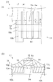
The thermal head X3 will be described with reference to FIG.

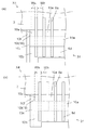
サーマルヘッドX3は、突出部10eのうち、上部コネクピン8a、または位置決め部10fに隣り合う部位に切欠部10iが形成されている。言い換えると、平面視して、突出部10eが、上部コネクタピン8a。または位置決め部10fと離間している。それにより、突出部10eと、上部コネクピン8a、または位置決め部10fとの間に隙間18が形成されている。   The thermal head X3 has a notch 10i formed in a portion adjacent to the upper connector pin 8a or the positioning portion 10f in the protruding portion 10e. In other words, the protrusion 10e is the upper connector pin 8a in plan view. Or it is spaced apart from the positioning part 10f. Thereby, the clearance gap 18 is formed between the protrusion part 10e, the upper connector pin 8a, or the positioning part 10f.

そして、図8(b)に示すように、隙間18には被覆部材12が配置されている。このように、切欠部10iにより、隙間18が形成され、隙間18に被覆部材12が配置されることにより、被覆部材12が上部コネクタピン8aの全体を被覆することができる。   As shown in FIG. 8B, the covering member 12 is disposed in the gap 18. As described above, the gap 18 is formed by the notch 10 i, and the covering member 12 is disposed in the gap 18, whereby the covering member 12 can cover the entire upper connector pin 8 a.

切欠部10iの幅(主走査方向における長さ)は、0.1〜0.3mmであることが好ましい。それにより、被覆部材12が下方へ流出することを抑えつつ、被覆部材12により上部コネクタピン8aを封止することができる。   The width of the notch 10i (length in the main scanning direction) is preferably 0.1 to 0.3 mm. Accordingly, the upper connector pin 8a can be sealed by the covering member 12 while suppressing the covering member 12 from flowing downward.

また、サーマルヘッドX3は、図8(b)に示すように、上部コネクタピン8aの上面8fが突出部10eの上面10gよりも高く配置され、上部コネクタピン8aの下面8eが突出部10eの下面10hよりも高く配置されるように構成されている。そして、上部コネクタピン8aの全体が被覆部材12により被覆されている。   In the thermal head X3, as shown in FIG. 8B, the upper surface 8f of the upper connector pin 8a is disposed higher than the upper surface 10g of the protruding portion 10e, and the lower surface 8e of the upper connector pin 8a is lower than the lower surface of the protruding portion 10e. It is configured to be arranged higher than 10h. The entire upper connector pin 8 a is covered with the covering member 12.

このように、上部コネクタピン8aの下面8eが、突出部10eの上面10gと下面10hとの間に配置されることにより、突出部10eの側面と上部コネクタピン8aの側面とにより隙間18が形成されることとなる。そして、隙間18の幅は5〜20μmであるため、毛細管現象が働き、隙間18から被覆部材12が下方に流出する可能性を低減することができる。   As described above, the lower surface 8e of the upper connector pin 8a is disposed between the upper surface 10g and the lower surface 10h of the protruding portion 10e, so that a gap 18 is formed between the side surface of the protruding portion 10e and the side surface of the upper connector pin 8a. Will be. And since the width | variety of the clearance gap 18 is 5-20 micrometers, a capillary phenomenon works and it can reduce possibility that the coating | coated member 12 will flow out downward from the clearance gap 18. FIG.

また、上部コネクタピン8aの下面8eが、突出部10eの下面10hよりも高い位置に配置されていることから、上部コネクタピン8aの下面8eが隙間18より下方に配置されない構成となり、上部コネクタピン8aの下面8eにも被覆部材12を配置することができる。その結果、上部コネクタピン8aの封止性を向上させることができる。   Further, since the lower surface 8e of the upper connector pin 8a is disposed at a position higher than the lower surface 10h of the protruding portion 10e, the lower surface 8e of the upper connector pin 8a is not disposed below the gap 18, and the upper connector pin The covering member 12 can also be arranged on the lower surface 8e of 8a. As a result, the sealing performance of the upper connector pin 8a can be improved.

<第4の実施形態>
図9を用いてサーマルヘッドX4について説明する。
<Fourth Embodiment>
The thermal head X4 will be described with reference to FIG.

サーマルヘッドX4は、主走査方向における両端に位置する突出部10eにのみ、切欠部10iが設けられており、主走査方向における両端に位置する突出部10eの幅Waが、他の突出部10eの幅Wbよりも狭くなっている。そして、切欠部10iによって形成された隙間18には、被覆部材(不図示)が配置されている。   The thermal head X4 is provided with notches 10i only in the protrusions 10e located at both ends in the main scanning direction, and the width Wa of the protrusions 10e located at both ends in the main scanning direction is equal to that of the other protrusions 10e. It is narrower than the width Wb. A covering member (not shown) is disposed in the gap 18 formed by the notch 10i.

ここで、サーマルヘッドは、コネクタの着脱をする際に、主走査方向における両端部に大きな外力が加わることとなる。それにより、位置決め部に変形が生じて、基板との位置合わせに不具合が生じる場合、あるいはヘッド基体と位置決め部とが剥離する場合がある。   Here, when the connector is attached to or detached from the thermal head, a large external force is applied to both ends in the main scanning direction. As a result, deformation may occur in the positioning portion, which may cause a problem in alignment with the substrate, or the head base and the positioning portion may peel off.

これに対して、サーマルヘッドX4は、主走査方向における両端に位置する突出部10eの幅Waが、他の突出部10eの幅Wbよりも狭い構成を有している。それにより、主走査方向における両端に位置する突出部10eの周囲に多くの量の被覆部材が配置されることとなる。そのため、主走査方向における両端に位置する突出部10eと位置決め部10fとの接合強度を向上させることができ、位置決め部10fに変形が生じる可能性、あるいはヘッド基体3と位置決め部10fとの剥離を抑えることができる。   On the other hand, the thermal head X4 has a configuration in which the width Wa of the protrusions 10e located at both ends in the main scanning direction is narrower than the width Wb of the other protrusions 10e. Accordingly, a large amount of the covering member is disposed around the protruding portions 10e located at both ends in the main scanning direction. Therefore, it is possible to improve the bonding strength between the protruding portions 10e located at both ends in the main scanning direction and the positioning portion 10f, and the positioning portion 10f may be deformed, or the head base 3 and the positioning portion 10f are separated. Can be suppressed.

幅Waは、幅Wbの50〜90%であることが好ましい。それにより、被覆部材が下方に流出する可能性を低減しつつ、主走査方向における両端部の接合強度を向上させることができる。   The width Wa is preferably 50 to 90% of the width Wb. Accordingly, it is possible to improve the bonding strength at both ends in the main scanning direction while reducing the possibility that the covering member flows downward.

なお、図9(b)に示すように、切欠部10iは、突出部10eのうち、位置決め部10fに隣り合う部位、および上部コネクタピン8aに隣り合う部位に設けてもよい。その場合においても、同様の効果を奏することができる。   As shown in FIG. 9 (b), the notch 10i may be provided in a portion of the protruding portion 10e adjacent to the positioning portion 10f and a portion adjacent to the upper connector pin 8a. Even in that case, the same effect can be obtained.

<第5の実施形態>
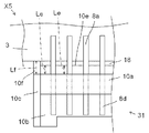
図10を用いてサーマルヘッドX5について説明する。サーマルヘッドX5は、突出部10eの突出長さLeが、サーマルヘッドX1と異なっており、その他の構成は同様である。
<Fifth Embodiment>
The thermal head X5 will be described with reference to FIG. In the thermal head X5, the protruding length Le of the protruding portion 10e is different from that of the thermal head X1, and other configurations are the same.

サーマルヘッドX5は、突出部10eの突出長さLeが、位置決め部10fの突出長さ
Lfよりも短い構成を有している。そのため、ヘッド基体3は、位置決め部10fにのみ突き当てられる構成となる。
The thermal head X5 has a configuration in which the protruding length Le of the protruding portion 10e is shorter than the protruding length Lf of the positioning portion 10f. Therefore, the head base 3 is configured to abut against only the positioning portion 10f.

それにより、ヘッド基体3を位置決め部10fのみにより位置決めすることから、ヘッド基体3の位置決めの精度を向上させることができる。つまり、突出部10eの突出長さLeは、製造過程においてばらつきが生じる可能性があり、突出長さLeのばらつきにより、ヘッド基体3の位置決めが不安定になる可能性がある。   Thereby, since the head base body 3 is positioned only by the positioning part 10f, the positioning accuracy of the head base body 3 can be improved. That is, the protrusion length Le of the protrusion 10e may vary in the manufacturing process, and the head base 3 may be unstable due to the variation of the protrusion length Le.

しかしながら、サーマルヘッドX5は、ヘッド基体3が位置決め部10fにのみ突き当てられる構成であるため、位置決め精度を向上させることができる。   However, since the thermal head X5 has a configuration in which the head base 3 is abutted only on the positioning portion 10f, the positioning accuracy can be improved.

また、サーマルヘッドX5は、突出部10eの突出長さLeが、位置決め部10fの突出長さLfよりも短い構成を有しているため、ヘッド基体3と突出部10eとの間に隙間18が形成され、隙間18には被覆部材(不図示)が充填されることとなる。そのため、ヘッド基体3とコネクタ31との接合強度を向上させることができる。   In addition, since the thermal head X5 has a configuration in which the protruding length Le of the protruding portion 10e is shorter than the protruding length Lf of the positioning portion 10f, there is a gap 18 between the head base 3 and the protruding portion 10e. The gap 18 is filled with a covering member (not shown). Therefore, the bonding strength between the head base 3 and the connector 31 can be improved.

以上、本発明の一実施形態について説明したが、本発明は上記実施形態に限定されるものではなく、その趣旨を逸脱しない限りにおいて種々の変更が可能である。例えば、第1の実施形態であるサーマルヘッドX1を用いたサーマルプリンタZ1を示したが、これに限定されるものではなく、サーマルヘッドX2〜X5をサーマルプリンタZ1に用いてもよい。また、複数の実施形態であるサーマルヘッドX1〜X5を組み合わせてもよい。   As mentioned above, although one Embodiment of this invention was described, this invention is not limited to the said embodiment, A various change is possible unless it deviates from the meaning. For example, although the thermal printer Z1 using the thermal head X1 according to the first embodiment is shown, the present invention is not limited to this, and the thermal heads X2 to X5 may be used for the thermal printer Z1. Moreover, you may combine the thermal heads X1-X5 which are some embodiment.

サーマルヘッドX1〜X5では、コネクタ31が、配列方向の中央部に配置された例を示したが、配列方向の両端部に設けてもよい。   In the thermal heads X <b> 1 to X <b> 5, the example in which the connector 31 is arranged at the center portion in the arrangement direction is shown, but it may be provided at both ends in the arrangement direction.

また、サーマルヘッドX1では、蓄熱層13に隆起部13bが形成され、隆起部13b上に電気抵抗層15が形成されているが、これに限定されるものではない。例えば、蓄熱層13に隆起部13bを形成せず、電気抵抗層15の発熱部9を、蓄熱層13の下地部13a上に配置してもよい。また、蓄熱層13を基板7の上面の全域にわたって設けてもよい。   In the thermal head X1, the raised portion 13b is formed on the heat storage layer 13 and the electric resistance layer 15 is formed on the raised portion 13b. However, the present invention is not limited to this. For example, the heat generating portion 9 of the electric resistance layer 15 may be disposed on the base portion 13 a of the heat storage layer 13 without forming the raised portion 13 b in the heat storage layer 13. Further, the heat storage layer 13 may be provided over the entire upper surface of the substrate 7.

また、サーマルヘッドX1では、電気抵抗層15上に共通電極17および個別電極19が形成されているが、共通電極17および個別電極19の双方が発熱部9(電気抵抗体)に接続されている限り、これに限定されるものではない。例えば、蓄熱層13上に共通電極17および個別電極19を形成し、共通電極17と個別電極19との間の領域のみに電気抵抗層15を形成することにより、発熱部9を構成してもよい。   In the thermal head X1, the common electrode 17 and the individual electrode 19 are formed on the electric resistance layer 15, but both the common electrode 17 and the individual electrode 19 are connected to the heat generating portion 9 (electric resistance body). As long as it is not limited to this. For example, even if the heat generating portion 9 is configured by forming the common electrode 17 and the individual electrode 19 on the heat storage layer 13 and forming the electric resistance layer 15 only in the region between the common electrode 17 and the individual electrode 19. Good.

さらにまた、電気抵抗層15を薄膜形成することにより、発熱部9の薄い薄膜ヘッドを例示して示したが、これに限定されるものではない。例えば、各種電極をパターニングした後に、電気抵抗層15を厚膜形成することにより、発熱部9の厚い厚膜ヘッドに本発明を用いてもよい。さらに、発熱部9を基板の端面に形成する端面ヘッドに本技術を用いてもよい。   Furthermore, the thin film head of the heat generating portion 9 is illustrated by forming the electric resistance layer 15 as a thin film. However, the present invention is not limited to this. For example, the present invention may be used for a thick film head of the heat generating portion 9 by forming a thick film of the electric resistance layer 15 after patterning various electrodes. Furthermore, you may use this technique for the end surface head which forms the heat-emitting part 9 in the end surface of a board | substrate.

さらにまた、コネクタピン8が、上部コネクタピン8aと下部コネクタピン8bとによりヘッド基体3を挟持するものを用いた例を示したがこれに限定されるものではない。コネクタピン8が上部コネクタピン8aのみを備え、上部コネクタピン8aが接続端子2上に配置されるものでもよい。   Furthermore, although the example which used the connector pin 8 which clamps the head base | substrate 3 with the upper connector pin 8a and the lower connector pin 8b was shown, it is not limited to this. The connector pin 8 may include only the upper connector pin 8a, and the upper connector pin 8a may be disposed on the connection terminal 2.

なお、被覆部材12を、駆動IC11を被覆するハードコート29とを同じ材料により形成してもよい。その場合、ハードコート29を印刷する際に、被覆部材12が形成され
る領域にも印刷して、ハードコート29と被覆部材12とを同時に形成してもよい。
The covering member 12 may be formed of the same material as the hard coat 29 that covers the driving IC 11. In that case, when the hard coat 29 is printed, the hard coat 29 and the covering member 12 may be formed simultaneously by printing also in the region where the covering member 12 is formed.

X1〜X5 サーマルヘッド
Z1 サーマルプリンタ
1 放熱体
1a 台部
2 接続端子
3 ヘッド基体
4 グランド電極
7 基板
8 コネクタピン
8a 上部コネクタピン
8b 下部コネクタピン
8c 連結部
8d 引き出し部
8e 下面
9 発熱部
10 ハウジング
10a 上壁
10b 下壁
10c 側壁
10d 突出部
10e 位置決め部
10f 上面
10g 下面
11 駆動IC
12 被覆部材
13 蓄熱層
14 隙間
15 電気抵抗層
16 隙間
17 共通電極
18 隙間
19 個別電極
21 IC−コネクタ接続電極
23 導電性接着剤
25 保護層
26 IC−IC接続電極
27 被覆部材
29 ハードコート
X1 to X5 Thermal head Z1 Thermal printer 1 Radiator 1a Base part 2 Connection terminal 3 Head base 4 Ground electrode 7 Substrate 8 Connector pin 8a Upper connector pin 8b Lower connector pin 8c Connection part 8d Lead part 8e Lower surface 9 Heating part 10 Housing 10a Upper wall 10b Lower wall 10c Side wall 10d Protruding portion 10e Positioning portion 10f Upper surface 10g Lower surface 11 Drive IC
DESCRIPTION OF SYMBOLS 12 Cover member 13 Heat storage layer 14 Gap 15 Electrical resistance layer 16 Gap 17 Common electrode 18 Gap 19 Individual electrode 21 IC-connector connection electrode 23 Conductive adhesive 25 Protective layer 26 IC-IC connection electrode 27 Cover member 29 Hard coat

Claims (7)

基板と、
該基板上に設けられた複数の発熱部と、
前記基板上に設けられ、前記発熱部に電気的に接続された電極と、
該電極に電気的に接続された複数のコネクタピン、および該コネクタピンを収容するハウジングを有したコネクタと、
前記コネクタピンと前記電極との接続部を被覆する被覆部材と、を備え、
前記ハウジングは、平面視して、隣り合う前記コネクタピン同士の間に向けて突出した突出部を有しており、
前記突出部に切欠部が設けられており、前記被覆部材が前記突出部と前記基板との間に配置されていることを特徴とするサーマルヘッド。
A substrate,
A plurality of heat generating portions provided on the substrate;
An electrode provided on the substrate and electrically connected to the heat generating portion;
A plurality of connector pins electrically connected to the electrodes, and a connector having a housing for accommodating the connector pins;
A covering member that covers a connection portion between the connector pin and the electrode;
The housing in a plan view, and have a protrusion protruding toward between the connector pins adjacent,
The thermal head is characterized in that a notch is provided in the protruding portion, and the covering member is disposed between the protruding portion and the substrate .
基板と、
該基板上に設けられた複数の発熱部と、
前記基板上に設けられ、前記発熱部に電気的に接続された電極と、
該電極に電気的に接続された複数のコネクタピン、および該コネクタピンを収容するハウジングを有したコネクタと、
前記コネクタピンと前記電極との接続部を被覆する被覆部材と、を備え、
前記ハウジングは、平面視して、隣り合う前記コネクタピン同士の間に向けて突出した突出部を有しており、
前記コネクタピンと前記突出部との間に隙間があることを特徴とするサーマルヘッド。
A substrate,
A plurality of heat generating portions provided on the substrate;
An electrode provided on the substrate and electrically connected to the heat generating portion;
A plurality of connector pins electrically connected to the electrodes, and a connector having a housing for accommodating the connector pins;
A covering member that covers a connection portion between the connector pin and the electrode;
The housing has a protruding portion that protrudes between the connector pins adjacent to each other in plan view,
A thermal head characterized in that there is a gap between the connector pin and the protrusion.
側面視して、前記コネクタピンは、上面が前記突出部の上面よりも高くに配置され、下面が前記突出部の下面よりも高くに配置されており、前記コネクタピンの全体が前記被覆部材により被覆されている、請求項に記載のサーマルヘッド。 When viewed from the side, the connector pin has an upper surface disposed higher than the upper surface of the protruding portion, a lower surface disposed higher than the lower surface of the protruding portion, and the entire connector pin is formed by the covering member. The thermal head according to claim 2 , wherein the thermal head is coated. 基板と、
該基板上に設けられた複数の発熱部と、
前記基板上に設けられ、前記発熱部に電気的に接続された電極と、
該電極に電気的に接続された複数のコネクタピン、および該コネクタピンを収容するハウジングを有したコネクタと、
前記コネクタピンと前記電極との接続部を被覆する被覆部材と、を備え、
前記ハウジングは、平面視して、隣り合う前記コネクタピン同士の間に向けて突出した
突出部を有しており、
前記ハウジングの側壁と隣り合うように設けられた前記突出部の幅が、他の前記突出部の幅よりも狭いことを特徴とするサーマルヘッド。
A substrate,
A plurality of heat generating portions provided on the substrate;
An electrode provided on the substrate and electrically connected to the heat generating portion;
A plurality of connector pins electrically connected to the electrodes, and a connector having a housing for accommodating the connector pins;
A covering member that covers a connection portion between the connector pin and the electrode;
The housing protrudes between the adjacent connector pins in a plan view.
Has a protrusion,
Thermal head width of the projecting portion provided to be adjacent the side wall of said housing, and wherein the narrower than the width of the other of the projecting portion.
基板と、
該基板上に設けられた複数の発熱部と、
前記基板上に設けられ、前記発熱部に電気的に接続された電極と、
該電極に電気的に接続された複数のコネクタピン、および該コネクタピンを収容するハウジングを有したコネクタと、
前記コネクタピンと前記電極との接続部を被覆する被覆部材と、を備え、
前記ハウジングは、平面視して、隣り合う前記コネクタピン同士の間に向けて突出した突出部を有しており、
前記コネクタが、前記ハウジングの側壁に設けられ、前記基板の位置決めを行うために前記基板に向けて突出した位置決め部をさらに備え、
前記突出部の突出長さが、前記位置決め部の突出長さと略等しいことを特徴とするサーマルヘッド。
A substrate,
A plurality of heat generating portions provided on the substrate;
An electrode provided on the substrate and electrically connected to the heat generating portion;
A plurality of connector pins electrically connected to the electrodes, and a connector having a housing for accommodating the connector pins;
A covering member that covers a connection portion between the connector pin and the electrode;
The housing has a protruding portion that protrudes between the connector pins adjacent to each other in plan view,
The connector is further provided with a positioning portion provided on a side wall of the housing and projecting toward the substrate to position the substrate;
The thermal head according to claim 1 , wherein a protruding length of the protruding portion is substantially equal to a protruding length of the positioning portion.
基板と、
該基板上に設けられた複数の発熱部と、
前記基板上に設けられ、前記発熱部に電気的に接続された電極と、
該電極に電気的に接続された複数のコネクタピン、および該コネクタピンを収容するハウジングを有したコネクタと、
前記コネクタピンと前記電極との接続部を被覆する被覆部材と、を備え、
前記ハウジングは、平面視して、隣り合う前記コネクタピン同士の間に向けて突出した突出部を有しており、
前記コネクタが、前記ハウジングの側壁に設けられ、前記基板の位置決めを行うために前記基板に向けて突出した位置決め部をさらに備え、
前記突出部の突出長さが、前記位置決め部の突出長さよりも短いことを特徴とするサーマルヘッド。
A substrate,
A plurality of heat generating portions provided on the substrate;
An electrode provided on the substrate and electrically connected to the heat generating portion;
A plurality of connector pins electrically connected to the electrodes, and a connector having a housing for accommodating the connector pins;
A covering member that covers a connection portion between the connector pin and the electrode;
The housing has a protruding portion that protrudes between the connector pins adjacent to each other in plan view,
The connector is further provided with a positioning portion provided on a side wall of the housing and projecting toward the substrate to position the substrate;
The thermal head characterized in that the protruding length of the protruding portion is shorter than the protruding length of the positioning portion.
請求項1乃至のうちいずれか1項に記載のサーマルヘッドと、
前記発熱部上に記録媒体を搬送する搬送機構と、
前記発熱部上に前記記録媒体を押圧するプラテンローラと、を備えることを特徴とするサーマルプリンタ。
The thermal head according to any one of claims 1 to 6 ,
A transport mechanism for transporting a recording medium onto the heat generating unit;
A thermal printer comprising: a platen roller that presses the recording medium onto the heat generating portion.
JP2013246250A 2013-11-28 2013-11-28 Thermal head and thermal printer Active JP6208564B2 (en)

Priority Applications (1)

Application Number Priority Date Filing Date Title
JP2013246250A JP6208564B2 (en) 2013-11-28 2013-11-28 Thermal head and thermal printer

Applications Claiming Priority (1)

Application Number Priority Date Filing Date Title
JP2013246250A JP6208564B2 (en) 2013-11-28 2013-11-28 Thermal head and thermal printer

Publications (2)

Publication Number Publication Date
JP2015104807A JP2015104807A (en) 2015-06-08
JP6208564B2 true JP6208564B2 (en) 2017-10-04

Family

ID=53435247

Family Applications (1)

Application Number Title Priority Date Filing Date
JP2013246250A Active JP6208564B2 (en) 2013-11-28 2013-11-28 Thermal head and thermal printer

Country Status (1)

Country Link
JP (1) JP6208564B2 (en)

Families Citing this family (1)

* Cited by examiner, † Cited by third party
Publication number Priority date Publication date Assignee Title
JP7267905B2 (en) * 2019-11-29 2023-05-02 京セラ株式会社 Thermal head and thermal printer

Family Cites Families (7)

* Cited by examiner, † Cited by third party
Publication number Priority date Publication date Assignee Title
JPH02248257A (en) * 1989-03-22 1990-10-04 Matsushita Electric Ind Co Ltd Thermal head
US5133670A (en) * 1991-03-18 1992-07-28 Kel Corporation Surface mount connector with contact aligning member
JP2818920B2 (en) * 1993-02-24 1998-10-30 ローム株式会社 Thermal head
JP2001105645A (en) * 1999-10-13 2001-04-17 Rohm Co Ltd Thermal print head and clip pin
JP2001113741A (en) * 1999-10-19 2001-04-24 Rohm Co Ltd Thermal printing head and production thereof
JP3929948B2 (en) * 2003-08-04 2007-06-13 矢崎総業株式会社 connector
JP3836850B2 (en) * 2004-04-28 2006-10-25 ローム株式会社 Thermal print head device

Also Published As

Publication number Publication date
JP2015104807A (en) 2015-06-08

Similar Documents

Publication Publication Date Title
JP6018288B2 (en) Thermal head and thermal printer
JP6219408B2 (en) Thermal head and thermal printer
JP6059412B1 (en) Thermal head and thermal printer
JP5952176B2 (en) Thermal head and thermal printer equipped with the same
JP6096997B2 (en) Thermal head and thermal printer
JP6419006B2 (en) Thermal head and thermal printer
WO2015029913A1 (en) Thermal head and thermal printer provided with same
JP6208564B2 (en) Thermal head and thermal printer
JP5489836B2 (en) Thermal head
JP6001465B2 (en) Thermal head and thermal printer equipped with the same
JP6208561B2 (en) Thermal head and thermal printer
JP2013028021A (en) Thermal head and thermal printer having the same
JP5937309B2 (en) Thermal head and thermal printer equipped with the same
JP6154334B2 (en) Thermal head and thermal printer
JP6046872B2 (en) Thermal head and thermal printer
JP5964745B2 (en) Thermal head and thermal printer equipped with the same
JP6352799B2 (en) Thermal head and thermal printer
JP6110198B2 (en) Thermal head and thermal printer
JP6075626B2 (en) Thermal head and thermal printer
JP6204084B2 (en) Thermal head and thermal printer
JP6426541B2 (en) Thermal head and thermal printer
JP6401066B2 (en) Thermal head and thermal printer equipped with the same
JP2015182240A (en) Thermal head and thermal printer
JP6352770B2 (en) Thermal head and thermal printer
JP2013176882A (en) Thermal head and thermal printer including the same

Legal Events

Date Code Title Description
A621 Written request for application examination

Free format text: JAPANESE INTERMEDIATE CODE: A621

Effective date: 20160516

A977 Report on retrieval

Free format text: JAPANESE INTERMEDIATE CODE: A971007

Effective date: 20170329

A131 Notification of reasons for refusal

Free format text: JAPANESE INTERMEDIATE CODE: A131

Effective date: 20170425

A521 Written amendment

Free format text: JAPANESE INTERMEDIATE CODE: A523

Effective date: 20170608

TRDD Decision of grant or rejection written
A01 Written decision to grant a patent or to grant a registration (utility model)

Free format text: JAPANESE INTERMEDIATE CODE: A01

Effective date: 20170808

A61 First payment of annual fees (during grant procedure)

Free format text: JAPANESE INTERMEDIATE CODE: A61

Effective date: 20170907

R150 Certificate of patent or registration of utility model

Ref document number: 6208564

Country of ref document: JP

Free format text: JAPANESE INTERMEDIATE CODE: R150