JP6489286B2 - インダクタモジュール - Google Patents
インダクタモジュール Download PDFInfo
- Publication number
- JP6489286B2 JP6489286B2 JP2018512042A JP2018512042A JP6489286B2 JP 6489286 B2 JP6489286 B2 JP 6489286B2 JP 2018512042 A JP2018512042 A JP 2018512042A JP 2018512042 A JP2018512042 A JP 2018512042A JP 6489286 B2 JP6489286 B2 JP 6489286B2
- Authority
- JP
- Japan
- Prior art keywords
- inductor
- chip
- flexible substrate
- module according
- dcdc converter
- Prior art date
- Legal status (The legal status is an assumption and is not a legal conclusion. Google has not performed a legal analysis and makes no representation as to the accuracy of the status listed.)
- Active
Links
Images


Classifications
-
- H—ELECTRICITY
- H01—ELECTRIC ELEMENTS
- H01F—MAGNETS; INDUCTANCES; TRANSFORMERS; SELECTION OF MATERIALS FOR THEIR MAGNETIC PROPERTIES
- H01F17/00—Fixed inductances of the signal type
- H01F17/0006—Printed inductances
- H01F17/0013—Printed inductances with stacked layers
-
- H—ELECTRICITY
- H01—ELECTRIC ELEMENTS
- H01F—MAGNETS; INDUCTANCES; TRANSFORMERS; SELECTION OF MATERIALS FOR THEIR MAGNETIC PROPERTIES
- H01F17/00—Fixed inductances of the signal type
- H01F17/04—Fixed inductances of the signal type with magnetic core
-
- H—ELECTRICITY
- H01—ELECTRIC ELEMENTS
- H01F—MAGNETS; INDUCTANCES; TRANSFORMERS; SELECTION OF MATERIALS FOR THEIR MAGNETIC PROPERTIES
- H01F27/00—Details of transformers or inductances, in general
- H01F27/28—Coils; Windings; Conductive connections
- H01F27/29—Terminals; Tapping arrangements for signal inductances
-
- H—ELECTRICITY
- H01—ELECTRIC ELEMENTS
- H01F—MAGNETS; INDUCTANCES; TRANSFORMERS; SELECTION OF MATERIALS FOR THEIR MAGNETIC PROPERTIES
- H01F37/00—Fixed inductances not covered by group H01F17/00
-
- H—ELECTRICITY
- H01—ELECTRIC ELEMENTS
- H01F—MAGNETS; INDUCTANCES; TRANSFORMERS; SELECTION OF MATERIALS FOR THEIR MAGNETIC PROPERTIES
- H01F41/00—Apparatus or processes specially adapted for manufacturing or assembling magnets, inductances or transformers; Apparatus or processes specially adapted for manufacturing materials characterised by their magnetic properties
- H01F41/02—Apparatus or processes specially adapted for manufacturing or assembling magnets, inductances or transformers; Apparatus or processes specially adapted for manufacturing materials characterised by their magnetic properties for manufacturing cores, coils, or magnets
- H01F41/04—Apparatus or processes specially adapted for manufacturing or assembling magnets, inductances or transformers; Apparatus or processes specially adapted for manufacturing materials characterised by their magnetic properties for manufacturing cores, coils, or magnets for manufacturing coils
- H01F41/041—Printed circuit coils
- H01F41/046—Printed circuit coils structurally combined with ferromagnetic material
-
- H—ELECTRICITY
- H01—ELECTRIC ELEMENTS
- H01L—SEMICONDUCTOR DEVICES NOT COVERED BY CLASS H10
- H01L23/00—Details of semiconductor or other solid state devices
- H01L23/48—Arrangements for conducting electric current to or from the solid state body in operation, e.g. leads, terminal arrangements ; Selection of materials therefor
- H01L23/488—Arrangements for conducting electric current to or from the solid state body in operation, e.g. leads, terminal arrangements ; Selection of materials therefor consisting of soldered or bonded constructions
- H01L23/498—Leads, i.e. metallisations or lead-frames on insulating substrates, e.g. chip carriers
- H01L23/4985—Flexible insulating substrates
-
- H—ELECTRICITY
- H01—ELECTRIC ELEMENTS
- H01L—SEMICONDUCTOR DEVICES NOT COVERED BY CLASS H10
- H01L23/00—Details of semiconductor or other solid state devices
- H01L23/58—Structural electrical arrangements for semiconductor devices not otherwise provided for, e.g. in combination with batteries
- H01L23/64—Impedance arrangements
- H01L23/645—Inductive arrangements
-
- H—ELECTRICITY
- H01—ELECTRIC ELEMENTS
- H01L—SEMICONDUCTOR DEVICES NOT COVERED BY CLASS H10
- H01L23/00—Details of semiconductor or other solid state devices
- H01L23/58—Structural electrical arrangements for semiconductor devices not otherwise provided for, e.g. in combination with batteries
- H01L23/64—Impedance arrangements
- H01L23/66—High-frequency adaptations
-
- H—ELECTRICITY
- H01—ELECTRIC ELEMENTS
- H01L—SEMICONDUCTOR DEVICES NOT COVERED BY CLASS H10
- H01L24/00—Arrangements for connecting or disconnecting semiconductor or solid-state bodies; Methods or apparatus related thereto
- H01L24/01—Means for bonding being attached to, or being formed on, the surface to be connected, e.g. chip-to-package, die-attach, "first-level" interconnects; Manufacturing methods related thereto
- H01L24/18—High density interconnect [HDI] connectors; Manufacturing methods related thereto
- H01L24/19—Manufacturing methods of high density interconnect preforms
-
- H—ELECTRICITY
- H01—ELECTRIC ELEMENTS
- H01L—SEMICONDUCTOR DEVICES NOT COVERED BY CLASS H10
- H01L24/00—Arrangements for connecting or disconnecting semiconductor or solid-state bodies; Methods or apparatus related thereto
- H01L24/01—Means for bonding being attached to, or being formed on, the surface to be connected, e.g. chip-to-package, die-attach, "first-level" interconnects; Manufacturing methods related thereto
- H01L24/18—High density interconnect [HDI] connectors; Manufacturing methods related thereto
- H01L24/20—Structure, shape, material or disposition of high density interconnect preforms
-
- H—ELECTRICITY
- H02—GENERATION; CONVERSION OR DISTRIBUTION OF ELECTRIC POWER
- H02M—APPARATUS FOR CONVERSION BETWEEN AC AND AC, BETWEEN AC AND DC, OR BETWEEN DC AND DC, AND FOR USE WITH MAINS OR SIMILAR POWER SUPPLY SYSTEMS; CONVERSION OF DC OR AC INPUT POWER INTO SURGE OUTPUT POWER; CONTROL OR REGULATION THEREOF
- H02M3/00—Conversion of DC power input into DC power output
- H02M3/02—Conversion of DC power input into DC power output without intermediate conversion into AC
- H02M3/04—Conversion of DC power input into DC power output without intermediate conversion into AC by static converters
- H02M3/10—Conversion of DC power input into DC power output without intermediate conversion into AC by static converters using discharge tubes with control electrode or semiconductor devices with control electrode
- H02M3/145—Conversion of DC power input into DC power output without intermediate conversion into AC by static converters using discharge tubes with control electrode or semiconductor devices with control electrode using devices of a triode or transistor type requiring continuous application of a control signal
- H02M3/155—Conversion of DC power input into DC power output without intermediate conversion into AC by static converters using discharge tubes with control electrode or semiconductor devices with control electrode using devices of a triode or transistor type requiring continuous application of a control signal using semiconductor devices only
-
- H—ELECTRICITY
- H04—ELECTRIC COMMUNICATION TECHNIQUE
- H04B—TRANSMISSION
- H04B5/00—Near-field transmission systems, e.g. inductive or capacitive transmission systems
- H04B5/20—Near-field transmission systems, e.g. inductive or capacitive transmission systems characterised by the transmission technique; characterised by the transmission medium
- H04B5/24—Inductive coupling
- H04B5/26—Inductive coupling using coils
-
- H—ELECTRICITY
- H04—ELECTRIC COMMUNICATION TECHNIQUE
- H04B—TRANSMISSION
- H04B5/00—Near-field transmission systems, e.g. inductive or capacitive transmission systems
- H04B5/40—Near-field transmission systems, e.g. inductive or capacitive transmission systems characterised by components specially adapted for near-field transmission
- H04B5/43—Antennas
-
- H—ELECTRICITY
- H04—ELECTRIC COMMUNICATION TECHNIQUE
- H04B—TRANSMISSION
- H04B5/00—Near-field transmission systems, e.g. inductive or capacitive transmission systems
- H04B5/40—Near-field transmission systems, e.g. inductive or capacitive transmission systems characterised by components specially adapted for near-field transmission
- H04B5/48—Transceivers
-
- H—ELECTRICITY
- H01—ELECTRIC ELEMENTS
- H01F—MAGNETS; INDUCTANCES; TRANSFORMERS; SELECTION OF MATERIALS FOR THEIR MAGNETIC PROPERTIES
- H01F17/00—Fixed inductances of the signal type
- H01F17/04—Fixed inductances of the signal type with magnetic core
- H01F2017/048—Fixed inductances of the signal type with magnetic core with encapsulating core, e.g. made of resin and magnetic powder
-
- H—ELECTRICITY
- H01—ELECTRIC ELEMENTS
- H01L—SEMICONDUCTOR DEVICES NOT COVERED BY CLASS H10
- H01L2223/00—Details relating to semiconductor or other solid state devices covered by the group H01L23/00
- H01L2223/58—Structural electrical arrangements for semiconductor devices not otherwise provided for
- H01L2223/64—Impedance arrangements
- H01L2223/66—High-frequency adaptations
- H01L2223/6661—High-frequency adaptations for passive devices
- H01L2223/6677—High-frequency adaptations for passive devices for antenna, e.g. antenna included within housing of semiconductor device
-
- H—ELECTRICITY
- H01—ELECTRIC ELEMENTS
- H01L—SEMICONDUCTOR DEVICES NOT COVERED BY CLASS H10
- H01L2224/00—Indexing scheme for arrangements for connecting or disconnecting semiconductor or solid-state bodies and methods related thereto as covered by H01L24/00
- H01L2224/01—Means for bonding being attached to, or being formed on, the surface to be connected, e.g. chip-to-package, die-attach, "first-level" interconnects; Manufacturing methods related thereto
- H01L2224/02—Bonding areas; Manufacturing methods related thereto
- H01L2224/04—Structure, shape, material or disposition of the bonding areas prior to the connecting process
- H01L2224/04105—Bonding areas formed on an encapsulation of the semiconductor or solid-state body, e.g. bonding areas on chip-scale packages
-
- H—ELECTRICITY
- H01—ELECTRIC ELEMENTS
- H01L—SEMICONDUCTOR DEVICES NOT COVERED BY CLASS H10
- H01L2224/00—Indexing scheme for arrangements for connecting or disconnecting semiconductor or solid-state bodies and methods related thereto as covered by H01L24/00
- H01L2224/01—Means for bonding being attached to, or being formed on, the surface to be connected, e.g. chip-to-package, die-attach, "first-level" interconnects; Manufacturing methods related thereto
- H01L2224/10—Bump connectors; Manufacturing methods related thereto
- H01L2224/12—Structure, shape, material or disposition of the bump connectors prior to the connecting process
- H01L2224/12105—Bump connectors formed on an encapsulation of the semiconductor or solid-state body, e.g. bumps on chip-scale packages
-
- H—ELECTRICITY
- H01—ELECTRIC ELEMENTS
- H01L—SEMICONDUCTOR DEVICES NOT COVERED BY CLASS H10
- H01L2224/00—Indexing scheme for arrangements for connecting or disconnecting semiconductor or solid-state bodies and methods related thereto as covered by H01L24/00
- H01L2224/01—Means for bonding being attached to, or being formed on, the surface to be connected, e.g. chip-to-package, die-attach, "first-level" interconnects; Manufacturing methods related thereto
- H01L2224/18—High density interconnect [HDI] connectors; Manufacturing methods related thereto
-
- H—ELECTRICITY
- H01—ELECTRIC ELEMENTS
- H01L—SEMICONDUCTOR DEVICES NOT COVERED BY CLASS H10
- H01L23/00—Details of semiconductor or other solid state devices
- H01L23/52—Arrangements for conducting electric current within the device in operation from one component to another, i.e. interconnections, e.g. wires, lead frames
- H01L23/538—Arrangements for conducting electric current within the device in operation from one component to another, i.e. interconnections, e.g. wires, lead frames the interconnection structure between a plurality of semiconductor chips being formed on, or in, insulating substrates
- H01L23/5389—Arrangements for conducting electric current within the device in operation from one component to another, i.e. interconnections, e.g. wires, lead frames the interconnection structure between a plurality of semiconductor chips being formed on, or in, insulating substrates the chips being integrally enclosed by the interconnect and support structures
-
- H—ELECTRICITY
- H01—ELECTRIC ELEMENTS
- H01L—SEMICONDUCTOR DEVICES NOT COVERED BY CLASS H10
- H01L2924/00—Indexing scheme for arrangements or methods for connecting or disconnecting semiconductor or solid-state bodies as covered by H01L24/00
- H01L2924/19—Details of hybrid assemblies other than the semiconductor or other solid state devices to be connected
- H01L2924/1901—Structure
- H01L2924/1904—Component type
- H01L2924/19041—Component type being a capacitor
-
- H—ELECTRICITY
- H01—ELECTRIC ELEMENTS
- H01L—SEMICONDUCTOR DEVICES NOT COVERED BY CLASS H10
- H01L2924/00—Indexing scheme for arrangements or methods for connecting or disconnecting semiconductor or solid-state bodies as covered by H01L24/00
- H01L2924/19—Details of hybrid assemblies other than the semiconductor or other solid state devices to be connected
- H01L2924/191—Disposition
- H01L2924/19101—Disposition of discrete passive components
- H01L2924/19105—Disposition of discrete passive components in a side-by-side arrangement on a common die mounting substrate
-
- H—ELECTRICITY
- H02—GENERATION; CONVERSION OR DISTRIBUTION OF ELECTRIC POWER
- H02M—APPARATUS FOR CONVERSION BETWEEN AC AND AC, BETWEEN AC AND DC, OR BETWEEN DC AND DC, AND FOR USE WITH MAINS OR SIMILAR POWER SUPPLY SYSTEMS; CONVERSION OF DC OR AC INPUT POWER INTO SURGE OUTPUT POWER; CONTROL OR REGULATION THEREOF
- H02M3/00—Conversion of DC power input into DC power output
- H02M3/003—Constructional details, e.g. physical layout, assembly, wiring or busbar connections
Landscapes
- Engineering & Computer Science (AREA)
- Power Engineering (AREA)
- Microelectronics & Electronic Packaging (AREA)
- Computer Hardware Design (AREA)
- General Physics & Mathematics (AREA)
- Condensed Matter Physics & Semiconductors (AREA)
- Physics & Mathematics (AREA)
- Computer Networks & Wireless Communication (AREA)
- Signal Processing (AREA)
- Manufacturing & Machinery (AREA)
- Dc-Dc Converters (AREA)
- Coils Or Transformers For Communication (AREA)
- Near-Field Transmission Systems (AREA)
Description
また、前記チップ状インダクタと前記IC素子とは平面視で重なる第1部分を有し、前記第1部分において、前記チップ状インダクタと前記フレキシブル基板との間には隙間を有していてもよい。
また、前記チップ状インダクタと前記チップ状コンデンサとは平面視で重なる第2部分を有し、前記第2部分において、前記チップ状インダクタと前記フレキシブル基板との間には隙間を有していてもよい。
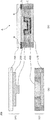
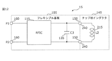
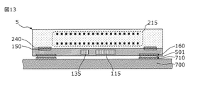
実施の形態1に係るインダクタモジュールは、IC素子とチップ状コンデンサとを内蔵した熱可塑性樹脂からなる絶縁性のフレキシブル基板上に、チップ状インダクタを搭載して構成される。
実施の形態2では、フレキシブル基板とチップ状インダクタとが、熱圧着処理により直接的かつ一体的に接合されてなるDCDCコンバータモジュールについて説明する。
実施の形態3では、チップ状インダクタに、スイッチングIC素子に対するノイズ抑制のための構造を追加したDCDCコンバータモジュールについて説明する。
実施の形態4に係るインダクタモジュールは、実施の形態1のインダクタモジュールと同様、IC素子とチップ状コンデンサとを内蔵した熱可塑性樹脂からなる絶縁性のフレキシブル基板上に、チップ状インダクタを搭載して構成される。
2a 集合積層ブロック
11、13 DCDCコンバータ回路
15 RF回路
100、101、102、105 フレキシブル基板
101a 集合フレキシブル基板
110 スイッチングIC素子
115 RFIC素子
120、130、135 チップ状コンデンサ
140、141、142、145 チップ状インダクタ
141a 集合インダクタ基板
150、151、152、240、241、242、250 接続端子
160 入出力端子
170、220、221、222、225 面内導体
200 素体
210、215 コイル
230、231、232、235 層間導体
251 突状部
300 補助層
400 ビア導体
500、501 導電性接合材
601、602 圧着用治具
700 基板
710 接続パターン
Claims (12)
- 複数の熱可塑性樹脂層を積層してなる絶縁性のフレキシブル基板と、
前記フレキシブル基板に内蔵されたIC素子と、
前記フレキシブル基板に内蔵されたチップ状コンデンサと、
磁性体を素体とし、前記フレキシブル基板の一方主面に搭載されたチップ状インダクタと、
前記フレキシブル基板の他方主面に形成された入出力端子と、
を備え、
前記チップ状インダクタの前記素体は、磁性体セラミックで構成されている、
インダクタモジュール。 - 平面視で、前記チップ状インダクタの投影面内に前記IC素子が配置されている、
請求項1に記載のインダクタモジュール。 - 前記チップ状インダクタは前記フレキシブル基板に向かう一方主面に平面状電極を有し、当該平面状電極を介して前記フレキシブル基板と接続されている、
請求項1または2に記載のインダクタモジュール。 - 前記IC素子は、平面視で前記入出力端子と重ならない位置に配置されている、
請求項1から3の何れか1項に記載のインダクタモジュール。 - 前記IC素子と前記入出力端子とを結ぶ配線の一部は、前記チップ状インダクタの前記素体の内部に引回されている、
請求項1から4の何れか1項に記載のインダクタモジュール。 - 前記チップ状インダクタの前記素体と前記フレキシブル基板とが直接的に接合されている、
請求項1から5の何れか1項に記載のインダクタモジュール。 - 前記チップ状インダクタの前記フレキシブル基板とは反対側の他方主面に、補助層が配置されている、
請求項1から6の何れか1項に記載のインダクタモジュール。 - 前記チップ状インダクタと前記フレキシブル基板とは、平面視で同じ大きさに形成されている、
請求項1から7の何れか1項に記載のインダクタモジュール。 - 前記チップ状インダクタと前記IC素子とは平面視で重なる第1部分を有し、
前記第1部分において、前記チップ状インダクタと前記フレキシブル基板との間には隙間を有する、
請求項1から8の何れか1項に記載のインダクタモジュール。 - 前記チップ状インダクタと前記チップ状コンデンサとは平面視で重なる第2部分を有し、
前記第2部分において、前記チップ状インダクタと前記フレキシブル基板との間には隙間を有する、
請求項1から9の何れか1項に記載のインダクタモジュール。 - 前記IC素子はスイッチングIC素子、前記チップ状インダクタはチョークコイルであって、DCDCコンバータモジュールを構成している、
請求項1から10のいずれか1項に記載のインダクタモジュール。 - 前記IC素子はRFIC素子、前記チップ状インダクタはアンテナコイルであって、RFモジュールを構成している、
請求項1から10のいずれか1項に記載のインダクタモジュール。
Applications Claiming Priority (3)
| Application Number | Priority Date | Filing Date | Title |
|---|---|---|---|
| JP2016080685 | 2016-04-13 | ||
| JP2016080685 | 2016-04-13 | ||
| PCT/JP2017/014955 WO2017179612A1 (ja) | 2016-04-13 | 2017-04-12 | インダクタモジュール |
Publications (2)
| Publication Number | Publication Date |
|---|---|
| JPWO2017179612A1 JPWO2017179612A1 (ja) | 2018-11-08 |
| JP6489286B2 true JP6489286B2 (ja) | 2019-03-27 |
Family
ID=60042143
Family Applications (1)
| Application Number | Title | Priority Date | Filing Date |
|---|---|---|---|
| JP2018512042A Active JP6489286B2 (ja) | 2016-04-13 | 2017-04-12 | インダクタモジュール |
Country Status (4)
| Country | Link |
|---|---|
| US (1) | US20190006076A1 (ja) |
| JP (1) | JP6489286B2 (ja) |
| CN (1) | CN208862743U (ja) |
| WO (1) | WO2017179612A1 (ja) |
Families Citing this family (3)
| Publication number | Priority date | Publication date | Assignee | Title |
|---|---|---|---|---|
| US11513578B1 (en) * | 2020-02-03 | 2022-11-29 | Meta Platforms Technologies, Llc | Power management system for an artificial reality system |
| CN113284734B (zh) * | 2021-05-24 | 2022-08-19 | 深圳市信维通信股份有限公司 | 摄像头用vcm线圈模组的制造工艺 |
| WO2024048718A1 (ja) * | 2022-09-02 | 2024-03-07 | 株式会社村田製作所 | Rfidモジュール |
Family Cites Families (13)
| Publication number | Priority date | Publication date | Assignee | Title |
|---|---|---|---|---|
| JP2841945B2 (ja) * | 1991-08-22 | 1998-12-24 | 富士通株式会社 | 半導体装置 |
| JP2003188538A (ja) * | 2001-12-18 | 2003-07-04 | Murata Mfg Co Ltd | 多層基板、および多層モジュール |
| JP2004015011A (ja) * | 2002-06-11 | 2004-01-15 | Murata Mfg Co Ltd | チップコイル |
| JP2004289912A (ja) * | 2003-03-20 | 2004-10-14 | Nec Tokin Corp | 薄型電源装置およびその製造方法 |
| JP4439336B2 (ja) * | 2004-06-02 | 2010-03-24 | 三洋電機株式会社 | 回路装置の製造方法 |
| JP2006128224A (ja) * | 2004-10-26 | 2006-05-18 | Neomax Co Ltd | 積層基板の製造方法及び積層基板 |
| JP2010021423A (ja) * | 2008-07-11 | 2010-01-28 | Tdk Corp | Ic内蔵基板及びその製造方法 |
| JP5229189B2 (ja) * | 2009-11-13 | 2013-07-03 | Tdk株式会社 | 電子部品モジュール |
| JP5605251B2 (ja) * | 2011-02-04 | 2014-10-15 | 株式会社村田製作所 | 無線icデバイス |
| JP5637004B2 (ja) * | 2011-02-23 | 2014-12-10 | 株式会社村田製作所 | 半導体集積回路モジュール、無線通信モジュール及び無線通信デバイス |
| JPWO2013157161A1 (ja) * | 2012-04-17 | 2015-12-21 | 株式会社村田製作所 | インダクタアレイチップ及びdc−dcコンバータ |
| WO2014199886A1 (ja) * | 2013-06-12 | 2014-12-18 | 株式会社村田製作所 | 通信装置および電子機器 |
| WO2015178061A1 (ja) * | 2014-05-21 | 2015-11-26 | 株式会社 村田製作所 | 回路モジュール |
-
2017
- 2017-04-12 JP JP2018512042A patent/JP6489286B2/ja active Active
- 2017-04-12 WO PCT/JP2017/014955 patent/WO2017179612A1/ja not_active Ceased
- 2017-04-12 CN CN201790000744.0U patent/CN208862743U/zh active Active
-
2018
- 2018-09-11 US US16/127,276 patent/US20190006076A1/en not_active Abandoned
Also Published As
| Publication number | Publication date |
|---|---|
| JPWO2017179612A1 (ja) | 2018-11-08 |
| WO2017179612A1 (ja) | 2017-10-19 |
| US20190006076A1 (en) | 2019-01-03 |
| CN208862743U (zh) | 2019-05-14 |
Similar Documents
| Publication | Publication Date | Title |
|---|---|---|
| US10389241B2 (en) | Power supply converter and method for manufacturing the same | |
| CN1531093B (zh) | 多输出超小型功率变换装置 | |
| JP6344521B2 (ja) | 積層コイル部品及びその製造方法、並びに、当該積層コイル部品を備えるdc−dcコンバータモジュール | |
| JP6819668B2 (ja) | モジュール部品、モジュール部品の製造方法、及び多層基板 | |
| US10645798B2 (en) | Composite component-embedded circuit board and composite component | |
| JP6432460B2 (ja) | Dc−dcコンバータ | |
| JP2009246159A (ja) | 多出力磁気誘導素子およびそれを備えた多出力超小型電力変換装置 | |
| JP2005073265A (ja) | 埋め込みpcb基板を用いたデュプレクサおよびその製造方法 | |
| CN115461863A (zh) | 集成电路 | |
| WO2017179590A1 (ja) | 受動素子アレイおよびプリント配線板 | |
| JP6489286B2 (ja) | インダクタモジュール | |
| JP3649214B2 (ja) | 超小型電力変換装置およびその製造方法 | |
| JPWO2017073438A1 (ja) | Lc複合デバイス、プロセッサおよびlc複合デバイスの製造方法 | |
| WO2017006784A1 (ja) | Dc-dcコンバータ | |
| JP6572791B2 (ja) | コイル複合部品及び多層基板、ならびに、コイル複合部品の製造方法 | |
| JP5429649B2 (ja) | インダクタ内蔵部品及びこれを用いたdc−dcコンバータ | |
| JP2008066672A (ja) | 薄型磁気部品内蔵基板及びそれを用いたスイッチング電源モジュール | |
| WO2016199629A1 (ja) | セラミック多層基板の製造方法、dc-dcコンバータの製造方法、セラミック多層基板、及びdc-dcコンバータ | |
| JP6528617B2 (ja) | 回路素子内蔵基板及びdc−dcコンバータモジュール | |
| JP6269541B2 (ja) | Dc−dcコンバータモジュールおよび製造方法 | |
| JP4330850B2 (ja) | 薄型コイル部品の製造方法,薄型コイル部品及びそれを使用した回路装置 | |
| JP6707970B2 (ja) | Icチップ実装基板 | |
| JP4974009B2 (ja) | 電子部品 | |
| KR20150024642A (ko) | 인덕터 소자 및 이의 제조방법 | |
| KR20170027257A (ko) | 전력 변환 장치 |
Legal Events
| Date | Code | Title | Description |
|---|---|---|---|
| A521 | Request for written amendment filed |
Free format text: JAPANESE INTERMEDIATE CODE: A523 Effective date: 20180531 |
|
| A621 | Written request for application examination |
Free format text: JAPANESE INTERMEDIATE CODE: A621 Effective date: 20180531 |
|
| A131 | Notification of reasons for refusal |
Free format text: JAPANESE INTERMEDIATE CODE: A131 Effective date: 20181113 |
|
| A521 | Request for written amendment filed |
Free format text: JAPANESE INTERMEDIATE CODE: A523 Effective date: 20181225 |
|
| TRDD | Decision of grant or rejection written | ||
| A01 | Written decision to grant a patent or to grant a registration (utility model) |
Free format text: JAPANESE INTERMEDIATE CODE: A01 Effective date: 20190129 |
|
| A61 | First payment of annual fees (during grant procedure) |
Free format text: JAPANESE INTERMEDIATE CODE: A61 Effective date: 20190211 |
|
| R150 | Certificate of patent or registration of utility model |
Ref document number: 6489286 Country of ref document: JP Free format text: JAPANESE INTERMEDIATE CODE: R150 |