JP6395673B2 - 基板処理装置 - Google Patents
基板処理装置 Download PDFInfo
- Publication number
- JP6395673B2 JP6395673B2 JP2015140593A JP2015140593A JP6395673B2 JP 6395673 B2 JP6395673 B2 JP 6395673B2 JP 2015140593 A JP2015140593 A JP 2015140593A JP 2015140593 A JP2015140593 A JP 2015140593A JP 6395673 B2 JP6395673 B2 JP 6395673B2
- Authority
- JP
- Japan
- Prior art keywords
- cleaning liquid
- cleaning
- substrate
- liquid supply
- substrate processing
- Prior art date
- Legal status (The legal status is an assumption and is not a legal conclusion. Google has not performed a legal analysis and makes no representation as to the accuracy of the status listed.)
- Active
Links
Images


Classifications
-
- H—ELECTRICITY
- H01—ELECTRIC ELEMENTS
- H01L—SEMICONDUCTOR DEVICES NOT COVERED BY CLASS H10
- H01L21/00—Processes or apparatus adapted for the manufacture or treatment of semiconductor or solid state devices or of parts thereof
- H01L21/02—Manufacture or treatment of semiconductor devices or of parts thereof
- H01L21/027—Making masks on semiconductor bodies for further photolithographic processing not provided for in group H01L21/18 or H01L21/34
-
- H—ELECTRICITY
- H01—ELECTRIC ELEMENTS
- H01L—SEMICONDUCTOR DEVICES NOT COVERED BY CLASS H10
- H01L21/00—Processes or apparatus adapted for the manufacture or treatment of semiconductor or solid state devices or of parts thereof
- H01L21/02—Manufacture or treatment of semiconductor devices or of parts thereof
- H01L21/04—Manufacture or treatment of semiconductor devices or of parts thereof the devices having potential barriers, e.g. a PN junction, depletion layer or carrier concentration layer
- H01L21/18—Manufacture or treatment of semiconductor devices or of parts thereof the devices having potential barriers, e.g. a PN junction, depletion layer or carrier concentration layer the devices having semiconductor bodies comprising elements of Group IV of the Periodic Table or AIIIBV compounds with or without impurities, e.g. doping materials
- H01L21/30—Treatment of semiconductor bodies using processes or apparatus not provided for in groups H01L21/20 - H01L21/26
- H01L21/302—Treatment of semiconductor bodies using processes or apparatus not provided for in groups H01L21/20 - H01L21/26 to change their surface-physical characteristics or shape, e.g. etching, polishing, cutting
- H01L21/304—Mechanical treatment, e.g. grinding, polishing, cutting
Landscapes
- Engineering & Computer Science (AREA)
- Physics & Mathematics (AREA)
- Condensed Matter Physics & Semiconductors (AREA)
- General Physics & Mathematics (AREA)
- Manufacturing & Machinery (AREA)
- Computer Hardware Design (AREA)
- Microelectronics & Electronic Packaging (AREA)
- Power Engineering (AREA)
- Cleaning Or Drying Semiconductors (AREA)
- Exposure Of Semiconductors, Excluding Electron Or Ion Beam Exposure (AREA)
Description
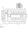
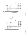
2 搬入出ステーション
3 処理ステーション
4 制御装置
16 処理ユニット
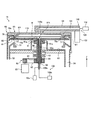
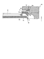
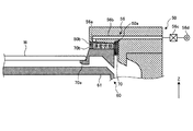
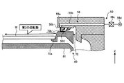
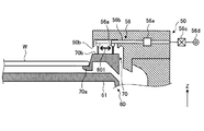
50 回収カップ
50a 窪み
50b 下面
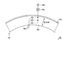
56 洗浄液供給部
60 回転プレート
70 回転リング
70b 平坦面
100 処理液供給部
W ウェハ
Claims (11)
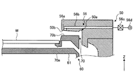
- 基板を回転させる回転プレートと、
前記基板の裏面に対して処理液を供給する処理液供給部と、
平坦面を有して前記基板の周縁部を取り囲むように前記回転プレートに連結されるリング部材と、
前記リング部材の上方に配置されるカバー部材と、
前記リング部材の平坦面に面する前記カバー部材の下面に前記リング部材の周方向に沿って複数設けられ、前記リング部材の平坦面に向けて洗浄液を供給する洗浄液供給部と
を備えることを特徴とする基板処理装置。 - 一連の基板処理を制御する制御部
を備え、
前記制御部は、
前記回転プレートを第1の回転数で回転させることにより前記リング部材の平坦面に前記洗浄液の液流を生じさせる第1洗浄処理を実行するよう制御し、
前記制御部はさらに、
前記回転プレートを回転させながら前記洗浄液供給部から供給される前記洗浄液の流量、流速および前記回転プレートの回転数のうちの少なくともいずれかを制御することにより、前記リング部材の平坦面と前記カバー部材の下面との間を液密状態にする液密洗浄処理を実行するよう制御すること
を特徴とする請求項1に記載の基板処理装置。 - 前記制御部は、
前記回転プレートを前記第1の回転数よりも大きい第2の回転数で回転させることにより前記洗浄液を飛散させて前記カバー部材の下面へ衝突させる第2洗浄処理を実行するよう制御すること
を特徴とする請求項2に記載の基板処理装置。 - 前記制御部は、
前記回転プレートを前記第2の回転数よりも大きい第3の回転数で回転させることにより前記カバー部材の下面の奥側へ前記洗浄液を到達させる第3洗浄処理を実行するよう制御すること
を特徴とする請求項3に記載の基板処理装置。 - 前記制御部は、
前記第1洗浄処理、前記第2洗浄処理、前記第3洗浄処理の順序で連続的に洗浄処理を実行するよう制御すること
を特徴とする請求項4に記載の基板処理装置。 - 前記制御部は、
前記第1洗浄処理、前記第2洗浄処理、前記第3洗浄処理のうち少なくとも1つの洗浄処理を実行した後、前記液密洗浄処理を実行するよう制御すること
を特徴とする請求項4または5に記載の基板処理装置。 - 基板を回転させる回転プレートと、
前記基板の裏面に対して処理液を供給する処理液供給部と、
平坦面を有して前記基板の周縁部を取り囲むように前記回転プレートに連結されるリング部材と、
前記リング部材の上方に配置されるカバー部材と、
前記リング部材の平坦面に向けて洗浄液を供給する洗浄液供給部と、
一連の基板処理を制御する制御部と
を備え、
前記制御部は、
前記回転プレートを第1の回転数で回転させることにより前記リング部材の平坦面に前記洗浄液の液流を生じさせる第1洗浄処理を実行するよう制御し、
前記制御部はさらに、
前記洗浄液供給部から供給される前記洗浄液の流量、流速および前記回転プレートの回転数のうちの少なくともいずれかを制御することにより、前記リング部材の平坦面と前記カバー部材の下面との間を液密状態にする液密洗浄処理を実行するよう制御すること
を特徴とする基板処理装置。 - 前記洗浄液供給部の前記リング部材に対する角度を変更させる変更機構
をさらに備え、
前記制御部は、
前記変更機構を用いて前記角度を変更させつつ、前記洗浄液供給部から前記リング部材に対して前記洗浄液を供給すること
を特徴とする請求項7に記載の基板処理装置。 - 前記洗浄液供給部は、不活性ガスを供給可能に設けられ、
前記制御部は、
前記洗浄液供給部に前記洗浄液を供給させた後、前記洗浄液供給部に前記不活性ガスを供給させること
を特徴とする請求項7または8に記載の基板処理装置。 - 前記洗浄液供給部は、略等間隔で少なくとも30個設けられること
を特徴とする請求項1〜9のいずれか一つに記載の基板処理装置。 - 前記回転プレート側に設けられ、該回転プレート側から前記洗浄液を前記洗浄液供給部と並行して供給する第2の洗浄液供給部
を備えることを特徴とする請求項1〜10のいずれか一つに記載の基板処理装置。
Priority Applications (2)
| Application Number | Priority Date | Filing Date | Title |
|---|---|---|---|
| JP2015140593A JP6395673B2 (ja) | 2015-07-14 | 2015-07-14 | 基板処理装置 |
| PCT/JP2016/066804 WO2017010191A1 (ja) | 2015-07-14 | 2016-06-06 | 基板処理装置及び記憶媒体 |
Applications Claiming Priority (1)
| Application Number | Priority Date | Filing Date | Title |
|---|---|---|---|
| JP2015140593A JP6395673B2 (ja) | 2015-07-14 | 2015-07-14 | 基板処理装置 |
Publications (2)
| Publication Number | Publication Date |
|---|---|
| JP2017022317A JP2017022317A (ja) | 2017-01-26 |
| JP6395673B2 true JP6395673B2 (ja) | 2018-09-26 |
Family
ID=57756873
Family Applications (1)
| Application Number | Title | Priority Date | Filing Date |
|---|---|---|---|
| JP2015140593A Active JP6395673B2 (ja) | 2015-07-14 | 2015-07-14 | 基板処理装置 |
Country Status (2)
| Country | Link |
|---|---|
| JP (1) | JP6395673B2 (ja) |
| WO (1) | WO2017010191A1 (ja) |
Families Citing this family (4)
| Publication number | Priority date | Publication date | Assignee | Title |
|---|---|---|---|---|
| JP7337634B2 (ja) * | 2019-09-30 | 2023-09-04 | 芝浦メカトロニクス株式会社 | 基板処理装置及び基板処理方法 |
| JP7557332B2 (ja) * | 2020-10-09 | 2024-09-27 | 東京エレクトロン株式会社 | 基板洗浄装置、基板洗浄方法及びコンピュータ読み取り可能な記録媒体 |
| JP7680318B2 (ja) * | 2021-09-24 | 2025-05-20 | 株式会社Screenホールディングス | 基板処理装置 |
| JP7664894B2 (ja) * | 2021-09-28 | 2025-04-18 | 花王株式会社 | 衛生処理箇所の決定方法 |
Family Cites Families (5)
| Publication number | Priority date | Publication date | Assignee | Title |
|---|---|---|---|---|
| JP2814184B2 (ja) * | 1993-08-23 | 1998-10-22 | 東京エレクトロン株式会社 | 塗布装置 |
| JP3518953B2 (ja) * | 1996-06-28 | 2004-04-12 | 大日本スクリーン製造株式会社 | 回転式基板処理装置 |
| JP3917384B2 (ja) * | 2001-02-15 | 2007-05-23 | 大日本スクリーン製造株式会社 | 基板処理装置および基板洗浄装置 |
| JP6022430B2 (ja) * | 2012-11-21 | 2016-11-09 | 東京エレクトロン株式会社 | 基板処理装置 |
| JP5996425B2 (ja) * | 2012-12-28 | 2016-09-21 | 東京エレクトロン株式会社 | 基板処理装置を洗浄するための洗浄治具および洗浄方法、および基板処理システム |
-
2015
- 2015-07-14 JP JP2015140593A patent/JP6395673B2/ja active Active
-
2016
- 2016-06-06 WO PCT/JP2016/066804 patent/WO2017010191A1/ja not_active Ceased
Also Published As
| Publication number | Publication date |
|---|---|
| JP2017022317A (ja) | 2017-01-26 |
| WO2017010191A1 (ja) | 2017-01-19 |
Similar Documents
| Publication | Publication Date | Title |
|---|---|---|
| TWI538044B (zh) | 用來清洗基板處理裝置的清洗治具及清洗方法、與基板處理系統 | |
| TWI656570B (zh) | Substrate liquid processing device, substrate liquid processing method, and memory medium | |
| JP5726686B2 (ja) | 液処理装置、及び液処理装置の制御方法 | |
| JP5797532B2 (ja) | 有機溶剤を含有する現像液を用いた現像処理方法及び現像処理装置 | |
| KR102294642B1 (ko) | 액 처리 장치 | |
| JP5705666B2 (ja) | 基板処理方法、基板処理システム及び基板処理プログラムを記憶したコンピュータ読み取り可能な記憶媒体 | |
| JP6395673B2 (ja) | 基板処理装置 | |
| JP6961362B2 (ja) | 基板処理装置 | |
| JP4757882B2 (ja) | 基板洗浄装置、基板洗浄方法、基板処理システムならびに記録媒体 | |
| JP5084656B2 (ja) | 現像処理方法及び現像処理装置 | |
| KR20210088644A (ko) | 기판 처리 장치 및 기판 처리 장치의 세정 방법 | |
| KR20210028788A (ko) | 기판 처리 장치 및 방법 | |
| KR20200021681A (ko) | 기판 처리 장치 | |
| JP3958572B2 (ja) | 基板処理装置及び基板処理方法 | |
| JP6049825B2 (ja) | 有機溶剤を含有する現像液を用いた現像処理方法及び現像処理装置 | |
| JP2018129476A (ja) | 基板処理装置 | |
| JP6914050B2 (ja) | 基板処理装置 | |
| KR20200013403A (ko) | 액 공급 유닛 및 기판 처리 장치 | |
| JP5372836B2 (ja) | 液処理方法、その液処理方法を実行させるためのプログラムを記録した記録媒体及び液処理装置 | |
| JP6986399B2 (ja) | 基板処理装置、基板処理方法および記憶媒体 | |
| JP5970102B2 (ja) | 液処理装置 | |
| JP7124946B2 (ja) | 液処理方法 | |
| JP6027640B2 (ja) | 基板処理システム | |
| KR20200021680A (ko) | 기판 처리 장치 | |
| JP4286822B2 (ja) | 洗浄処理装置 |
Legal Events
| Date | Code | Title | Description |
|---|---|---|---|
| A621 | Written request for application examination |
Free format text: JAPANESE INTERMEDIATE CODE: A621 Effective date: 20170725 |
|
| A131 | Notification of reasons for refusal |
Free format text: JAPANESE INTERMEDIATE CODE: A131 Effective date: 20180522 |
|
| A521 | Request for written amendment filed |
Free format text: JAPANESE INTERMEDIATE CODE: A523 Effective date: 20180719 |
|
| TRDD | Decision of grant or rejection written | ||
| A01 | Written decision to grant a patent or to grant a registration (utility model) |
Free format text: JAPANESE INTERMEDIATE CODE: A01 Effective date: 20180814 |
|
| A61 | First payment of annual fees (during grant procedure) |
Free format text: JAPANESE INTERMEDIATE CODE: A61 Effective date: 20180828 |
|
| R150 | Certificate of patent or registration of utility model |
Ref document number: 6395673 Country of ref document: JP Free format text: JAPANESE INTERMEDIATE CODE: R150 |
|
| R250 | Receipt of annual fees |
Free format text: JAPANESE INTERMEDIATE CODE: R250 |
|
| R250 | Receipt of annual fees |
Free format text: JAPANESE INTERMEDIATE CODE: R250 |
|
| R250 | Receipt of annual fees |
Free format text: JAPANESE INTERMEDIATE CODE: R250 |
|
| R250 | Receipt of annual fees |
Free format text: JAPANESE INTERMEDIATE CODE: R250 |
|
| R250 | Receipt of annual fees |
Free format text: JAPANESE INTERMEDIATE CODE: R250 |