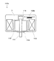
JP6371122B2 - パワー半導体装置および樹脂封止型モータ - Google Patents
パワー半導体装置および樹脂封止型モータ Download PDFInfo
- Publication number
- JP6371122B2 JP6371122B2 JP2014117042A JP2014117042A JP6371122B2 JP 6371122 B2 JP6371122 B2 JP 6371122B2 JP 2014117042 A JP2014117042 A JP 2014117042A JP 2014117042 A JP2014117042 A JP 2014117042A JP 6371122 B2 JP6371122 B2 JP 6371122B2
- Authority
- JP
- Japan
- Prior art keywords
- chip
- size
- electrode pad
- semiconductor device
- power semiconductor
- Prior art date
- Legal status (The legal status is an assumption and is not a legal conclusion. Google has not performed a legal analysis and makes no representation as to the accuracy of the status listed.)
- Active
Links
Images
Classifications
-
- H—ELECTRICITY
- H01—ELECTRIC ELEMENTS
- H01L—SEMICONDUCTOR DEVICES NOT COVERED BY CLASS H10
- H01L2224/00—Indexing scheme for arrangements for connecting or disconnecting semiconductor or solid-state bodies and methods related thereto as covered by H01L24/00
- H01L2224/01—Means for bonding being attached to, or being formed on, the surface to be connected, e.g. chip-to-package, die-attach, "first-level" interconnects; Manufacturing methods related thereto
- H01L2224/10—Bump connectors; Manufacturing methods related thereto
- H01L2224/15—Structure, shape, material or disposition of the bump connectors after the connecting process
- H01L2224/16—Structure, shape, material or disposition of the bump connectors after the connecting process of an individual bump connector
- H01L2224/161—Disposition
- H01L2224/16151—Disposition the bump connector connecting between a semiconductor or solid-state body and an item not being a semiconductor or solid-state body, e.g. chip-to-substrate, chip-to-passive
- H01L2224/16221—Disposition the bump connector connecting between a semiconductor or solid-state body and an item not being a semiconductor or solid-state body, e.g. chip-to-substrate, chip-to-passive the body and the item being stacked
- H01L2224/16225—Disposition the bump connector connecting between a semiconductor or solid-state body and an item not being a semiconductor or solid-state body, e.g. chip-to-substrate, chip-to-passive the body and the item being stacked the item being non-metallic, e.g. insulating substrate with or without metallisation
-
- H—ELECTRICITY
- H01—ELECTRIC ELEMENTS
- H01L—SEMICONDUCTOR DEVICES NOT COVERED BY CLASS H10
- H01L2224/00—Indexing scheme for arrangements for connecting or disconnecting semiconductor or solid-state bodies and methods related thereto as covered by H01L24/00
- H01L2224/73—Means for bonding being of different types provided for in two or more of groups H01L2224/10, H01L2224/18, H01L2224/26, H01L2224/34, H01L2224/42, H01L2224/50, H01L2224/63, H01L2224/71
- H01L2224/732—Location after the connecting process
- H01L2224/73251—Location after the connecting process on different surfaces
- H01L2224/73253—Bump and layer connectors
-
- H—ELECTRICITY
- H01—ELECTRIC ELEMENTS
- H01L—SEMICONDUCTOR DEVICES NOT COVERED BY CLASS H10
- H01L2924/00—Indexing scheme for arrangements or methods for connecting or disconnecting semiconductor or solid-state bodies as covered by H01L24/00
- H01L2924/10—Details of semiconductor or other solid state devices to be connected
- H01L2924/11—Device type
- H01L2924/13—Discrete devices, e.g. 3 terminal devices
- H01L2924/1304—Transistor
- H01L2924/1305—Bipolar Junction Transistor [BJT]
- H01L2924/13055—Insulated gate bipolar transistor [IGBT]
-
- H—ELECTRICITY
- H01—ELECTRIC ELEMENTS
- H01L—SEMICONDUCTOR DEVICES NOT COVERED BY CLASS H10
- H01L2924/00—Indexing scheme for arrangements or methods for connecting or disconnecting semiconductor or solid-state bodies as covered by H01L24/00
- H01L2924/10—Details of semiconductor or other solid state devices to be connected
- H01L2924/11—Device type
- H01L2924/13—Discrete devices, e.g. 3 terminal devices
- H01L2924/1304—Transistor
- H01L2924/1306—Field-effect transistor [FET]
- H01L2924/13091—Metal-Oxide-Semiconductor Field-Effect Transistor [MOSFET]
Landscapes
- Inverter Devices (AREA)
Priority Applications (1)
| Application Number | Priority Date | Filing Date | Title |
|---|---|---|---|
| JP2014117042A JP6371122B2 (ja) | 2014-06-05 | 2014-06-05 | パワー半導体装置および樹脂封止型モータ |
Applications Claiming Priority (1)
| Application Number | Priority Date | Filing Date | Title |
|---|---|---|---|
| JP2014117042A JP6371122B2 (ja) | 2014-06-05 | 2014-06-05 | パワー半導体装置および樹脂封止型モータ |
Publications (3)
| Publication Number | Publication Date |
|---|---|
| JP2015230990A JP2015230990A (ja) | 2015-12-21 |
| JP2015230990A5 JP2015230990A5 (enExample) | 2017-04-13 |
| JP6371122B2 true JP6371122B2 (ja) | 2018-08-08 |
Family
ID=54887621
Family Applications (1)
| Application Number | Title | Priority Date | Filing Date |
|---|---|---|---|
| JP2014117042A Active JP6371122B2 (ja) | 2014-06-05 | 2014-06-05 | パワー半導体装置および樹脂封止型モータ |
Country Status (1)
| Country | Link |
|---|---|
| JP (1) | JP6371122B2 (enExample) |
Cited By (2)
| Publication number | Priority date | Publication date | Assignee | Title |
|---|---|---|---|---|
| US11626221B2 (en) | 2021-06-16 | 2023-04-11 | Fuji Electric Co., Ltd. | Resistance element and its manufacturing method |
| US20240112996A1 (en) * | 2019-10-24 | 2024-04-04 | Rohm Co., Ltd. | Semiconductor device |
Families Citing this family (1)
| Publication number | Priority date | Publication date | Assignee | Title |
|---|---|---|---|---|
| JP7290960B2 (ja) * | 2019-03-11 | 2023-06-14 | ローム株式会社 | 半導体装置 |
Family Cites Families (12)
| Publication number | Priority date | Publication date | Assignee | Title |
|---|---|---|---|---|
| JPH04134862U (ja) * | 1991-06-04 | 1992-12-15 | 沖電気工業株式会社 | 混成集積回路装置 |
| JPH06181286A (ja) * | 1992-12-14 | 1994-06-28 | Toshiba Corp | 半導体装置 |
| US5977640A (en) * | 1998-06-26 | 1999-11-02 | International Business Machines Corporation | Highly integrated chip-on-chip packaging |
| JP3815933B2 (ja) * | 1999-12-10 | 2006-08-30 | ローム株式会社 | 半導体装置及びその製造方法 |
| JP3503133B2 (ja) * | 1999-12-10 | 2004-03-02 | 日本電気株式会社 | 電子デバイス集合体と電子デバイスの接続方法 |
| JP2002170920A (ja) * | 2000-12-04 | 2002-06-14 | Nec Eng Ltd | フリップチップ装置 |
| JP3723869B2 (ja) * | 2001-03-30 | 2005-12-07 | 株式会社日立製作所 | 半導体装置 |
| JP2003152158A (ja) * | 2001-11-09 | 2003-05-23 | Matsushita Electric Ind Co Ltd | 半導体素子を実装した電子部品及びその製造方法 |
| JP2003258197A (ja) * | 2002-03-07 | 2003-09-12 | Seiko Instruments Inc | 半導体装置 |
| JP2003319615A (ja) * | 2002-04-23 | 2003-11-07 | Matsushita Electric Ind Co Ltd | モールド型モータ |
| JP2004146728A (ja) * | 2002-10-28 | 2004-05-20 | Sony Corp | 半導体装置とその製造方法 |
| JP5966287B2 (ja) * | 2011-09-15 | 2016-08-10 | 大日本印刷株式会社 | サスペンション用基板、サスペンション、素子付サスペンション、ハードディスクドライブ、およびサスペンション用基板の製造方法 |
-
2014
- 2014-06-05 JP JP2014117042A patent/JP6371122B2/ja active Active
Cited By (2)
| Publication number | Priority date | Publication date | Assignee | Title |
|---|---|---|---|---|
| US20240112996A1 (en) * | 2019-10-24 | 2024-04-04 | Rohm Co., Ltd. | Semiconductor device |
| US11626221B2 (en) | 2021-06-16 | 2023-04-11 | Fuji Electric Co., Ltd. | Resistance element and its manufacturing method |
Also Published As
| Publication number | Publication date |
|---|---|
| JP2015230990A (ja) | 2015-12-21 |
Similar Documents
| Publication | Publication Date | Title |
|---|---|---|
| CN108364942B (zh) | 半导体器件 | |
| KR101524545B1 (ko) | 전력 소자 패키지 및 그 제조 방법 | |
| TWI731129B (zh) | 電子裝置 | |
| JP6791621B2 (ja) | 半導体装置 | |
| JP5381444B2 (ja) | パワーモジュール | |
| JP7391957B2 (ja) | 半導体装置 | |
| JP7199167B2 (ja) | パワー半導体モジュール、電力変換装置、およびパワー半導体モジュールの製造方法 | |
| KR20090104477A (ko) | 반도체 소자 패키지 | |
| US9105601B2 (en) | Power module package | |
| JP7561677B2 (ja) | 電力半導体装置、電力半導体装置の製造方法及び電力変換装置 | |
| JP2002083927A (ja) | 半導体装置 | |
| JP6354674B2 (ja) | 半導体装置 | |
| JP2022133480A (ja) | 半導体装置 | |
| JP6371122B2 (ja) | パワー半導体装置および樹脂封止型モータ | |
| US12438063B2 (en) | Electronic module including a semiconductor package disposed on an interposer layer | |
| US11810835B2 (en) | Intelligent power module packaging structure | |
| JP2016115727A (ja) | 半導体装置 | |
| WO2022259426A1 (ja) | 半導体モジュールおよび電力変換装置 | |
| JPWO2018180580A1 (ja) | 半導体装置および電力変換装置 | |
| JP2010225952A (ja) | 半導体モジュール | |
| KR20210151194A (ko) | 반도체 장치 및 반도체 장치의 제조 방법 | |
| JP6383265B2 (ja) | 半導体装置 | |
| JP2007073674A (ja) | 半導体装置 | |
| JP7479771B2 (ja) | 半導体装置、半導体装置の製造方法及び電力変換装置 | |
| WO2013105456A1 (ja) | 回路基板および電子デバイス |
Legal Events
| Date | Code | Title | Description |
|---|---|---|---|
| A521 | Request for written amendment filed |
Free format text: JAPANESE INTERMEDIATE CODE: A523 Effective date: 20170306 |
|
| A621 | Written request for application examination |
Free format text: JAPANESE INTERMEDIATE CODE: A621 Effective date: 20170306 |
|
| A977 | Report on retrieval |
Free format text: JAPANESE INTERMEDIATE CODE: A971007 Effective date: 20171122 |
|
| A131 | Notification of reasons for refusal |
Free format text: JAPANESE INTERMEDIATE CODE: A131 Effective date: 20171205 |
|
| A521 | Request for written amendment filed |
Free format text: JAPANESE INTERMEDIATE CODE: A523 Effective date: 20180125 |
|
| TRDD | Decision of grant or rejection written | ||
| A01 | Written decision to grant a patent or to grant a registration (utility model) |
Free format text: JAPANESE INTERMEDIATE CODE: A01 Effective date: 20180703 |
|
| A61 | First payment of annual fees (during grant procedure) |
Free format text: JAPANESE INTERMEDIATE CODE: A61 Effective date: 20180712 |
|
| R150 | Certificate of patent or registration of utility model |
Ref document number: 6371122 Country of ref document: JP Free format text: JAPANESE INTERMEDIATE CODE: R150 |
|
| S111 | Request for change of ownership or part of ownership |
Free format text: JAPANESE INTERMEDIATE CODE: R313117 |
|
| R350 | Written notification of registration of transfer |
Free format text: JAPANESE INTERMEDIATE CODE: R350 |
|
| S533 | Written request for registration of change of name |
Free format text: JAPANESE INTERMEDIATE CODE: R313533 |
|
| R350 | Written notification of registration of transfer |
Free format text: JAPANESE INTERMEDIATE CODE: R350 |
