JP6227010B2 - 撮像装置、撮像システム、および、撮像装置の製造方法 - Google Patents
撮像装置、撮像システム、および、撮像装置の製造方法 Download PDFInfo
- Publication number
- JP6227010B2 JP6227010B2 JP2015554350A JP2015554350A JP6227010B2 JP 6227010 B2 JP6227010 B2 JP 6227010B2 JP 2015554350 A JP2015554350 A JP 2015554350A JP 2015554350 A JP2015554350 A JP 2015554350A JP 6227010 B2 JP6227010 B2 JP 6227010B2
- Authority
- JP
- Japan
- Prior art keywords
- region
- gate region
- channel
- forming
- side portion
- Prior art date
- Legal status (The legal status is an assumption and is not a legal conclusion. Google has not performed a legal analysis and makes no representation as to the accuracy of the status listed.)
- Expired - Fee Related
Links
Images


Classifications
-
- H—ELECTRICITY
- H10—SEMICONDUCTOR DEVICES; ELECTRIC SOLID-STATE DEVICES NOT OTHERWISE PROVIDED FOR
- H10F—INORGANIC SEMICONDUCTOR DEVICES SENSITIVE TO INFRARED RADIATION, LIGHT, ELECTROMAGNETIC RADIATION OF SHORTER WAVELENGTH OR CORPUSCULAR RADIATION
- H10F39/00—Integrated devices, or assemblies of multiple devices, comprising at least one element covered by group H10F30/00, e.g. radiation detectors comprising photodiode arrays
- H10F39/10—Integrated devices
- H10F39/12—Image sensors
- H10F39/196—Junction field effect transistor [JFET] image sensors; Static induction transistor [SIT] image sensors
-
- H—ELECTRICITY
- H10—SEMICONDUCTOR DEVICES; ELECTRIC SOLID-STATE DEVICES NOT OTHERWISE PROVIDED FOR
- H10D—INORGANIC ELECTRIC SEMICONDUCTOR DEVICES
- H10D30/00—Field-effect transistors [FET]
- H10D30/01—Manufacture or treatment
- H10D30/051—Manufacture or treatment of FETs having PN junction gates
- H10D30/0512—Manufacture or treatment of FETs having PN junction gates of FETs having PN homojunction gates
- H10D30/0515—Manufacture or treatment of FETs having PN junction gates of FETs having PN homojunction gates of vertical FETs having PN homojunction gates
-
- H—ELECTRICITY
- H10—SEMICONDUCTOR DEVICES; ELECTRIC SOLID-STATE DEVICES NOT OTHERWISE PROVIDED FOR
- H10D—INORGANIC ELECTRIC SEMICONDUCTOR DEVICES
- H10D30/00—Field-effect transistors [FET]
- H10D30/80—FETs having rectifying junction gate electrodes
- H10D30/83—FETs having PN junction gate electrodes
- H10D30/831—Vertical FETs having PN junction gate electrodes
-
- H—ELECTRICITY
- H10—SEMICONDUCTOR DEVICES; ELECTRIC SOLID-STATE DEVICES NOT OTHERWISE PROVIDED FOR
- H10D—INORGANIC ELECTRIC SEMICONDUCTOR DEVICES
- H10D62/00—Semiconductor bodies, or regions thereof, of devices having potential barriers
- H10D62/10—Shapes, relative sizes or dispositions of the regions of the semiconductor bodies; Shapes of the semiconductor bodies
- H10D62/17—Semiconductor regions connected to electrodes not carrying current to be rectified, amplified or switched, e.g. channel regions
- H10D62/213—Channel regions of field-effect devices
- H10D62/221—Channel regions of field-effect devices of FETs
- H10D62/328—Channel regions of field-effect devices of FETs having PN junction gates
-
- H—ELECTRICITY
- H10—SEMICONDUCTOR DEVICES; ELECTRIC SOLID-STATE DEVICES NOT OTHERWISE PROVIDED FOR
- H10D—INORGANIC ELECTRIC SEMICONDUCTOR DEVICES
- H10D62/00—Semiconductor bodies, or regions thereof, of devices having potential barriers
- H10D62/10—Shapes, relative sizes or dispositions of the regions of the semiconductor bodies; Shapes of the semiconductor bodies
- H10D62/17—Semiconductor regions connected to electrodes not carrying current to be rectified, amplified or switched, e.g. channel regions
- H10D62/343—Gate regions of field-effect devices having PN junction gates
-
- H—ELECTRICITY
- H10—SEMICONDUCTOR DEVICES; ELECTRIC SOLID-STATE DEVICES NOT OTHERWISE PROVIDED FOR
- H10F—INORGANIC SEMICONDUCTOR DEVICES SENSITIVE TO INFRARED RADIATION, LIGHT, ELECTROMAGNETIC RADIATION OF SHORTER WAVELENGTH OR CORPUSCULAR RADIATION
- H10F30/00—Individual radiation-sensitive semiconductor devices in which radiation controls the flow of current through the devices, e.g. photodetectors
- H10F30/20—Individual radiation-sensitive semiconductor devices in which radiation controls the flow of current through the devices, e.g. photodetectors the devices having potential barriers, e.g. phototransistors
- H10F30/21—Individual radiation-sensitive semiconductor devices in which radiation controls the flow of current through the devices, e.g. photodetectors the devices having potential barriers, e.g. phototransistors the devices being sensitive to infrared, visible or ultraviolet radiation
- H10F30/28—Individual radiation-sensitive semiconductor devices in which radiation controls the flow of current through the devices, e.g. photodetectors the devices having potential barriers, e.g. phototransistors the devices being sensitive to infrared, visible or ultraviolet radiation the devices being characterised by field-effect operation, e.g. junction field-effect phototransistors
- H10F30/285—Individual radiation-sensitive semiconductor devices in which radiation controls the flow of current through the devices, e.g. photodetectors the devices having potential barriers, e.g. phototransistors the devices being sensitive to infrared, visible or ultraviolet radiation the devices being characterised by field-effect operation, e.g. junction field-effect phototransistors the devices having PN homojunction gates
- H10F30/2863—Field-effect phototransistors having PN homojunction gates
-
- H—ELECTRICITY
- H10—SEMICONDUCTOR DEVICES; ELECTRIC SOLID-STATE DEVICES NOT OTHERWISE PROVIDED FOR
- H10F—INORGANIC SEMICONDUCTOR DEVICES SENSITIVE TO INFRARED RADIATION, LIGHT, ELECTROMAGNETIC RADIATION OF SHORTER WAVELENGTH OR CORPUSCULAR RADIATION
- H10F39/00—Integrated devices, or assemblies of multiple devices, comprising at least one element covered by group H10F30/00, e.g. radiation detectors comprising photodiode arrays
- H10F39/011—Manufacture or treatment of image sensors covered by group H10F39/12
- H10F39/014—Manufacture or treatment of image sensors covered by group H10F39/12 of CMOS image sensors
-
- H—ELECTRICITY
- H10—SEMICONDUCTOR DEVICES; ELECTRIC SOLID-STATE DEVICES NOT OTHERWISE PROVIDED FOR
- H10F—INORGANIC SEMICONDUCTOR DEVICES SENSITIVE TO INFRARED RADIATION, LIGHT, ELECTROMAGNETIC RADIATION OF SHORTER WAVELENGTH OR CORPUSCULAR RADIATION
- H10F39/00—Integrated devices, or assemblies of multiple devices, comprising at least one element covered by group H10F30/00, e.g. radiation detectors comprising photodiode arrays
- H10F39/80—Constructional details of image sensors
- H10F39/802—Geometry or disposition of elements in pixels, e.g. address-lines or gate electrodes
-
- H—ELECTRICITY
- H10—SEMICONDUCTOR DEVICES; ELECTRIC SOLID-STATE DEVICES NOT OTHERWISE PROVIDED FOR
- H10D—INORGANIC ELECTRIC SEMICONDUCTOR DEVICES
- H10D84/00—Integrated devices formed in or on semiconductor substrates that comprise only semiconducting layers, e.g. on Si wafers or on GaAs-on-Si wafers
- H10D84/01—Manufacture or treatment
- H10D84/0123—Integrating together multiple components covered by H10D12/00 or H10D30/00, e.g. integrating multiple IGBTs
-
- H—ELECTRICITY
- H10—SEMICONDUCTOR DEVICES; ELECTRIC SOLID-STATE DEVICES NOT OTHERWISE PROVIDED FOR
- H10D—INORGANIC ELECTRIC SEMICONDUCTOR DEVICES
- H10D84/00—Integrated devices formed in or on semiconductor substrates that comprise only semiconducting layers, e.g. on Si wafers or on GaAs-on-Si wafers
- H10D84/01—Manufacture or treatment
- H10D84/02—Manufacture or treatment characterised by using material-based technologies
- H10D84/03—Manufacture or treatment characterised by using material-based technologies using Group IV technology, e.g. silicon technology or silicon-carbide [SiC] technology
- H10D84/038—Manufacture or treatment characterised by using material-based technologies using Group IV technology, e.g. silicon technology or silicon-carbide [SiC] technology using silicon technology, e.g. SiGe
-
- H—ELECTRICITY
- H10—SEMICONDUCTOR DEVICES; ELECTRIC SOLID-STATE DEVICES NOT OTHERWISE PROVIDED FOR
- H10F—INORGANIC SEMICONDUCTOR DEVICES SENSITIVE TO INFRARED RADIATION, LIGHT, ELECTROMAGNETIC RADIATION OF SHORTER WAVELENGTH OR CORPUSCULAR RADIATION
- H10F39/00—Integrated devices, or assemblies of multiple devices, comprising at least one element covered by group H10F30/00, e.g. radiation detectors comprising photodiode arrays
- H10F39/10—Integrated devices
- H10F39/12—Image sensors
Landscapes
- Solid State Image Pick-Up Elements (AREA)
- Junction Field-Effect Transistors (AREA)
- Transforming Light Signals Into Electric Signals (AREA)
Description
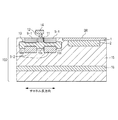
1 N型半導体領域(光電変換部)
2 P型半導体領域(光電変換部)
9 ゲート領域
10 チャネル領域
17 第1のマスク
18 第2のマスク
209 第1の開口
210 第2の開口
Claims (12)
- 半導体基板に配された接合型電界効果トランジスタをそれぞれが含む複数の画素を備える撮像装置の製造方法であって、
第1の開口を規定する第1のマスクを用いて前記半導体基板に不純物を導入することにより、前記接合型電界効果トランジスタのゲート領域を形成する工程と、
第2の開口を規定する第2のマスクを用いて前記半導体基板に不純物を導入することにより、前記接合型電界効果トランジスタのチャネル領域を形成する工程と、を有し、
前記第2の開口は、前記チャネル領域のソース側の部分に対応するソース側部分と前記チャネル領域のドレイン側の部分に対応するドレイン側部分とを含み、
前記半導体基板の表面と平行な面への前記第1の開口の正射影と、前記面への前記第2の開口の正射影とが交差し、
前記面への前記ソース側部分の正射影、および、前記面への前記ドレイン側部分の正射影が、それぞれ、前記第1のマスクの前記面への正射影と重なり、
前記ゲート領域は、互いに異なる深さに形成される表面ゲート領域と埋め込みゲート領域とを含み、
前記ゲート領域を形成する工程は、それぞれが前記第1のマスクを用い、かつ、イオン注入エネルギーが互いに異なる複数のイオン注入工程を含み、
前記表面ゲート領域と前記埋め込みゲート領域との中間の深さに前記チャネル領域を形成し、
前記第1の開口は、前記第1のマスクによって分割された複数の開口を含み、
前記面への前記複数の開口の正射影のそれぞれが、前記第2の開口の正射影と交差し、
前記ソース側部分の正射影は、前記第1のマスクのうち、前記複数の開口の間にある部分の前記面への正射影と重なり、
前記複数の開口に対応して形成される複数の前記埋め込みゲート領域の間の空乏層によって、前記チャネル領域の前記ソース側の部分と前記埋め込みゲート領域の下の半導体領域との間にポテンシャルバリアが形成されるように、前記複数の開口の間隔が定められる、
ことを特徴とする撮像装置の製造方法。 - 前記表面ゲート領域と前記埋め込みゲート領域とが互いに電気的に接続される深さに形成されるように、前記イオン注入エネルギーを選択する、
ことを特徴とする請求項1に記載の撮像装置の製造方法。 - 前記表面ゲート領域と前記埋め込みゲート領域とを電気的に接続する第1の半導体領域を形成する工程をさらに有する、
ことを特徴とする請求項1に記載の撮像装置の製造方法。 - 前記ゲート領域を形成する工程において、前記複数の開口に対応する複数のゲート領域を形成し、
前記複数のゲート領域を互いに電気的に接続する第2の半導体領域を形成する工程をさらに有する、
ことを特徴とする請求項1乃至請求項3のいずれか一項に記載の撮像装置の製造方法。 - 前記第2の半導体領域を形成する工程は、第3の開口を規定する第3のマスクを用いて行われ、
前記第1の開口の正射影が、前記面への前記第3の開口の正射影と部分的に重なり、
前記第2の開口の正射影の全体が、前記第3のマスクの前記面への正射影と重なる、
ことを特徴とする請求項4に記載の撮像装置の製造方法。 - 前記チャネル領域のソース側の部分と電気的に接続されるソース領域を形成する工程をさらに含む、
ことを特徴とする請求項1乃至請求項5のいずれか一項に記載の撮像装置の製造方法。 - 前記半導体基板の表面と平行な面への前記第1の開口の正射影と、前記面への前記第2の開口の正射影との重なった部分によって、前記接合型電界効果トランジスタのチャネル長およびチャネル幅を規定する、
ことを特徴とする請求項1乃至請求項6のいずれか一項に記載の撮像装置の製造方法。 - 前記第1の開口の正射影の外縁は互いに平行な2つの線分を含み、
前記第2の開口の正射影の外縁は互いに平行な2つの線分を含む、
ことを特徴とする請求項1乃至請求項7のいずれか一項に記載の撮像装置の製造方法。 - 半導体基板に配された接合型電界効果トランジスタをそれぞれが含む複数の画素を備える撮像装置の形成方法であって、
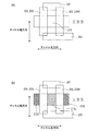
前記半導体基板に前記接合型電界効果トランジスタのゲート領域を形成する工程と、
前記半導体基板に前記接合型電界効果トランジスタのチャネル領域を形成する工程と、を有し、
前記半導体基板の表面と平行な面への、前記ゲート領域を形成する工程において不純物が導入される第1領域の正射影と、前記面への、前記チャネル領域を形成する工程において不純物が導入される第2領域の正射影とが交差し、
前記面において、前記第2領域の正射影のソース側の部分、および、ドレイン側の部分が、それぞれ、前記第1領域の正射影から突出し、
前記ゲート領域は、互いに異なる深さに形成される表面ゲート領域と埋め込みゲート領域とを含み、
前記表面ゲート領域と前記埋め込みゲート領域との中間の深さに前記チャネル領域を形成し、
前記第1領域の正射影は、間隔をおいて配された複数の部分を含み、
前記第2領域の正射影の前記ソース側部分は、前記複数の部分の間にあり、
前記複数の部分に対応して形成される複数の前記埋め込みゲート領域の間の空乏層によって、前記チャネル領域の前記ソース側の部分と前記埋め込みゲート領域の下の半導体領域との間にポテンシャルバリアが形成されるように、前記複数の部分の間隔が定められる、
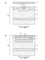
ことを特徴とする撮像装置の形成方法。 - 半導体基板に配された接合型電界効果トランジスタをそれぞれが含む複数の画素を備える撮像装置であって、
前記接合型電界効果トランジスタは、それぞれ異なる深さに配された、表面ゲート領域と埋め込みゲート領域とチャネル領域とを含み、
前記チャネル領域は、前記表面ゲート領域と前記埋め込みゲート領域との中間の深さに配され、
前記半導体基板の表面と平行な面への前記表面ゲート領域の正射影、および、前記埋め込みゲート領域の正射影が、それぞれ、前記面への前記チャネル領域の正射影と交差し、
前記表面ゲート領域および前記埋め込みゲート領域のそれぞれが、前記接合型電界効果トランジスタのソース領域を挟むように配され、かつ、互いに電気的に接続された複数の領域を含み、
前記面への前記複数の領域の正射影のそれぞれが、前記チャネル領域の正射影と交差し、
前記埋め込みゲート領域の前記複数の領域の間の空乏層によって、前記ソース領域と前記埋め込みゲート領域の下の半導体領域との間にポテンシャルバリアが形成される、
ことを特徴とする撮像装置。 - 請求項10に記載の撮像装置と、
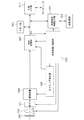
被写体の光学像を前記撮像装置に結像させるレンズと、
を備えた撮像システム。 - 請求項10に記載の撮像装置と、
前記撮像装置から出力される信号を処理する信号処理装置と、
を備えた撮像システム。
Applications Claiming Priority (1)
| Application Number | Priority Date | Filing Date | Title |
|---|---|---|---|
| PCT/JP2013/084566 WO2015097771A1 (ja) | 2013-12-25 | 2013-12-25 | 撮像装置、撮像システム、および、撮像装置の製造方法 |
Publications (2)
| Publication Number | Publication Date |
|---|---|
| JPWO2015097771A1 JPWO2015097771A1 (ja) | 2017-03-23 |
| JP6227010B2 true JP6227010B2 (ja) | 2017-11-08 |
Family
ID=53400937
Family Applications (1)
| Application Number | Title | Priority Date | Filing Date |
|---|---|---|---|
| JP2015554350A Expired - Fee Related JP6227010B2 (ja) | 2013-12-25 | 2013-12-25 | 撮像装置、撮像システム、および、撮像装置の製造方法 |
Country Status (7)
| Country | Link |
|---|---|
| US (1) | US9577004B2 (ja) |
| EP (1) | EP3091576A4 (ja) |
| JP (1) | JP6227010B2 (ja) |
| KR (1) | KR101866673B1 (ja) |
| CN (1) | CN105830219B (ja) |
| RU (1) | RU2638108C1 (ja) |
| WO (1) | WO2015097771A1 (ja) |
Families Citing this family (3)
| Publication number | Priority date | Publication date | Assignee | Title |
|---|---|---|---|---|
| US10446695B2 (en) | 2015-10-21 | 2019-10-15 | United Silicone Carbide, Inc. | Planar multi-implanted JFET |
| US9653618B1 (en) | 2015-10-21 | 2017-05-16 | United Silicon Carbide, Inc. | Planar triple-implanted JFET |
| KR102667510B1 (ko) * | 2019-07-29 | 2024-05-22 | 에스케이하이닉스 주식회사 | 이미지 센싱 장치 |
Family Cites Families (22)
| Publication number | Priority date | Publication date | Assignee | Title |
|---|---|---|---|---|
| JPS5664470A (en) * | 1979-10-31 | 1981-06-01 | Pioneer Electronic Corp | Junction type field-effect transistor |
| JPS5941871A (ja) * | 1982-08-31 | 1984-03-08 | Matsushita Electronics Corp | 接合型電界効果半導体装置 |
| JPS59108461A (ja) * | 1982-12-14 | 1984-06-22 | Olympus Optical Co Ltd | 固体撮像装置 |
| US5089862A (en) * | 1986-05-12 | 1992-02-18 | Warner Jr Raymond M | Monocrystalline three-dimensional integrated circuit |
| JP3109274B2 (ja) * | 1992-08-31 | 2000-11-13 | 日本電気株式会社 | 半導体装置およびその製造方法 |
| JP2002231730A (ja) * | 2001-02-01 | 2002-08-16 | Sumitomo Electric Ind Ltd | 横型接合型電界効果トランジスタおよびその製造方法 |
| JP3812421B2 (ja) * | 2001-06-14 | 2006-08-23 | 住友電気工業株式会社 | 横型接合型電界効果トランジスタ |
| JP3925253B2 (ja) * | 2002-03-15 | 2007-06-06 | 住友電気工業株式会社 | 横型接合型電界効果トランジスタおよびその製造方法 |
| US7180105B2 (en) * | 2004-02-09 | 2007-02-20 | International Rectifier Corporation | Normally off JFET |
| JP2005252083A (ja) * | 2004-03-05 | 2005-09-15 | Nikon Corp | 接合型電界効果トランジスタ、及び固体撮像装置 |
| JP2006179825A (ja) * | 2004-12-24 | 2006-07-06 | Nikon Corp | 増幅型固体撮像素子 |
| JP2006196789A (ja) * | 2005-01-14 | 2006-07-27 | Nikon Corp | 接合型電界効果トランジスタ及びその製造方法、並びに固体撮像素子 |
| JP2006351729A (ja) * | 2005-06-14 | 2006-12-28 | Canon Inc | 接合形電界効果トランジスタ及びその製造方法並びに固体撮像装置 |
| JP2007165736A (ja) * | 2005-12-16 | 2007-06-28 | Nikon Corp | Jfet(接合型電界効果トランジスタ)、及びこれを用いた固体撮像装置 |
| KR100776146B1 (ko) * | 2006-05-04 | 2007-11-15 | 매그나칩 반도체 유한회사 | 화소를 버스트 리셋 동작과 통합하여 개선된 성능을 갖는cmos이미지 센서 |
| JP2008108793A (ja) * | 2006-10-23 | 2008-05-08 | Sanyo Electric Co Ltd | 接合型fetおよびその製造方法 |
| US7727821B2 (en) * | 2007-05-01 | 2010-06-01 | Suvolta, Inc. | Image sensing cell, device, method of operation, and method of manufacture |
| KR100851495B1 (ko) * | 2007-05-14 | 2008-08-08 | 매그나칩 반도체 유한회사 | Jfet 및 수직적으로 집적된 리셋 다이오드를 갖는이미지 센서의 소형 픽셀 |
| JP2009043923A (ja) * | 2007-08-08 | 2009-02-26 | Sanyo Electric Co Ltd | 半導体装置及びその製造方法 |
| JP4759590B2 (ja) * | 2008-05-09 | 2011-08-31 | キヤノン株式会社 | 光電変換装置及びそれを用いた撮像システム |
| JP5495524B2 (ja) * | 2008-08-18 | 2014-05-21 | キヤノン株式会社 | 光電変換装置 |
| CN102610623A (zh) * | 2012-01-11 | 2012-07-25 | 格科微电子(上海)有限公司 | 图像传感器及源跟随器 |
-
2013
- 2013-12-25 JP JP2015554350A patent/JP6227010B2/ja not_active Expired - Fee Related
- 2013-12-25 EP EP13900494.9A patent/EP3091576A4/en not_active Withdrawn
- 2013-12-25 RU RU2016130101A patent/RU2638108C1/ru not_active IP Right Cessation
- 2013-12-25 KR KR1020167019228A patent/KR101866673B1/ko not_active Expired - Fee Related
- 2013-12-25 CN CN201380081797.6A patent/CN105830219B/zh not_active Expired - Fee Related
- 2013-12-25 WO PCT/JP2013/084566 patent/WO2015097771A1/ja not_active Ceased
-
2014
- 2014-12-18 US US14/576,028 patent/US9577004B2/en not_active Expired - Fee Related
Also Published As
| Publication number | Publication date |
|---|---|
| EP3091576A4 (en) | 2017-11-29 |
| US9577004B2 (en) | 2017-02-21 |
| WO2015097771A1 (ja) | 2015-07-02 |
| RU2638108C1 (ru) | 2017-12-11 |
| EP3091576A1 (en) | 2016-11-09 |
| KR101866673B1 (ko) | 2018-06-11 |
| CN105830219B (zh) | 2019-01-01 |
| CN105830219A (zh) | 2016-08-03 |
| WO2015097771A9 (ja) | 2016-01-07 |
| KR20160100354A (ko) | 2016-08-23 |
| JPWO2015097771A1 (ja) | 2017-03-23 |
| US20150179688A1 (en) | 2015-06-25 |
Similar Documents
| Publication | Publication Date | Title |
|---|---|---|
| US9466641B2 (en) | Solid-state imaging device | |
| TW201312740A (zh) | 固體攝像元件 | |
| JP5539373B2 (ja) | 固体撮像装置及びその製造方法 | |
| CN104916654A (zh) | 固态图像捕获装置、其制造方法和照相机 | |
| JP6227010B2 (ja) | 撮像装置、撮像システム、および、撮像装置の製造方法 | |
| JP6445799B2 (ja) | 光電変換装置 | |
| JP5717329B2 (ja) | 固体撮像装置及びその製造方法 | |
| CN104241305B (zh) | 光电转换设备以及光电转换设备的制造方法 | |
| JP2015125997A (ja) | 撮像装置、撮像システム、および、撮像装置の製造方法。 | |
| JP6265731B2 (ja) | 撮像装置、撮像システム、および、撮像装置の製造方法。 | |
| CN114846607B (zh) | 倍增型图像传感器 | |
| JP2016018823A (ja) | 固体撮像装置の製造方法 | |
| JP4586452B2 (ja) | 固体撮像装置 | |
| JP2016051813A (ja) | 半導体装置の製造方法、半導体装置、撮像装置および撮像装置の製造方法 | |
| JP2016051812A (ja) | 接合型電界効果トランジスタの製造方法、半導体装置の製造方法、撮像装置の製造方法、接合型電界効果トランジスタ及び撮像装置 |
Legal Events
| Date | Code | Title | Description |
|---|---|---|---|
| A621 | Written request for application examination |
Free format text: JAPANESE INTERMEDIATE CODE: A621 Effective date: 20161216 |
|
| A131 | Notification of reasons for refusal |
Free format text: JAPANESE INTERMEDIATE CODE: A131 Effective date: 20170328 |
|
| A521 | Request for written amendment filed |
Free format text: JAPANESE INTERMEDIATE CODE: A523 Effective date: 20170523 |
|
| A131 | Notification of reasons for refusal |
Free format text: JAPANESE INTERMEDIATE CODE: A131 Effective date: 20170627 |
|
| A521 | Request for written amendment filed |
Free format text: JAPANESE INTERMEDIATE CODE: A523 Effective date: 20170828 |
|
| TRDD | Decision of grant or rejection written | ||
| A01 | Written decision to grant a patent or to grant a registration (utility model) |
Free format text: JAPANESE INTERMEDIATE CODE: A01 Effective date: 20170912 |
|
| A61 | First payment of annual fees (during grant procedure) |
Free format text: JAPANESE INTERMEDIATE CODE: A61 Effective date: 20171010 |
|
| R151 | Written notification of patent or utility model registration |
Ref document number: 6227010 Country of ref document: JP Free format text: JAPANESE INTERMEDIATE CODE: R151 |
|
| LAPS | Cancellation because of no payment of annual fees |