US9577004B2 - Imaging apparatus, imaging system and manufacturing method of imaging apparatus - Google Patents

Imaging apparatus, imaging system and manufacturing method of imaging apparatus Download PDF

Info

Publication number
US9577004B2
US9577004B2 US14/576,028 US201414576028A US9577004B2 US 9577004 B2 US9577004 B2 US 9577004B2 US 201414576028 A US201414576028 A US 201414576028A US 9577004 B2 US9577004 B2 US 9577004B2
Authority
US
United States
Prior art keywords
region
gate region
channel
orthogonal projection
imaging apparatus
Prior art date
Legal status (The legal status is an assumption and is not a legal conclusion. Google has not performed a legal analysis and makes no representation as to the accuracy of the status listed.)
Expired - Fee Related
Application number
US14/576,028
Other versions
US20150179688A1 (en
Inventor
Mahito Shinohara
Masahiro Kobayashi
Masatsugu Itahashi
Current Assignee (The listed assignees may be inaccurate. Google has not performed a legal analysis and makes no representation or warranty as to the accuracy of the list.)
Canon Inc
Original Assignee
Canon Inc
Priority date (The priority date is an assumption and is not a legal conclusion. Google has not performed a legal analysis and makes no representation as to the accuracy of the date listed.)
Filing date
Publication date
Application filed by Canon Inc filed Critical Canon Inc
Assigned to CANON KABUSHIKI KAISHA reassignment CANON KABUSHIKI KAISHA ASSIGNMENT OF ASSIGNORS INTEREST (SEE DOCUMENT FOR DETAILS). Assignors: ITAHASHI, MASATSUGU, KOBAYASHI, MASAHIRO, SHINOHARA, MAHITO
Publication of US20150179688A1 publication Critical patent/US20150179688A1/en
Application granted granted Critical
Publication of US9577004B2 publication Critical patent/US9577004B2/en
Expired - Fee Related legal-status Critical Current
Anticipated expiration legal-status Critical

Links

Images

Classifications

    • HELECTRICITY
    • H01ELECTRIC ELEMENTS
    • H01LSEMICONDUCTOR DEVICES NOT COVERED BY CLASS H10
    • H01L27/00Devices consisting of a plurality of semiconductor or other solid-state components formed in or on a common substrate
    • H01L27/14Devices consisting of a plurality of semiconductor or other solid-state components formed in or on a common substrate including semiconductor components sensitive to infrared radiation, light, electromagnetic radiation of shorter wavelength or corpuscular radiation and specially adapted either for the conversion of the energy of such radiation into electrical energy or for the control of electrical energy by such radiation
    • H01L27/144Devices controlled by radiation
    • H01L27/146Imager structures
    • H01L27/14683Processes or apparatus peculiar to the manufacture or treatment of these devices or parts thereof
    • H01L27/14689MOS based technologies
    • HELECTRICITY
    • H01ELECTRIC ELEMENTS
    • H01LSEMICONDUCTOR DEVICES NOT COVERED BY CLASS H10
    • H01L27/00Devices consisting of a plurality of semiconductor or other solid-state components formed in or on a common substrate
    • H01L27/14Devices consisting of a plurality of semiconductor or other solid-state components formed in or on a common substrate including semiconductor components sensitive to infrared radiation, light, electromagnetic radiation of shorter wavelength or corpuscular radiation and specially adapted either for the conversion of the energy of such radiation into electrical energy or for the control of electrical energy by such radiation
    • H01L27/144Devices controlled by radiation
    • H01L27/146Imager structures
    • H01L27/14601Structural or functional details thereof
    • H01L27/14603Special geometry or disposition of pixel-elements, address-lines or gate-electrodes
    • HELECTRICITY
    • H01ELECTRIC ELEMENTS
    • H01LSEMICONDUCTOR DEVICES NOT COVERED BY CLASS H10
    • H01L27/00Devices consisting of a plurality of semiconductor or other solid-state components formed in or on a common substrate
    • H01L27/14Devices consisting of a plurality of semiconductor or other solid-state components formed in or on a common substrate including semiconductor components sensitive to infrared radiation, light, electromagnetic radiation of shorter wavelength or corpuscular radiation and specially adapted either for the conversion of the energy of such radiation into electrical energy or for the control of electrical energy by such radiation
    • H01L27/144Devices controlled by radiation
    • H01L27/146Imager structures
    • H01L27/14679Junction field effect transistor [JFET] imagers; static induction transistor [SIT] imagers
    • HELECTRICITY
    • H01ELECTRIC ELEMENTS
    • H01LSEMICONDUCTOR DEVICES NOT COVERED BY CLASS H10
    • H01L29/00Semiconductor devices adapted for rectifying, amplifying, oscillating or switching, or capacitors or resistors with at least one potential-jump barrier or surface barrier, e.g. PN junction depletion layer or carrier concentration layer; Details of semiconductor bodies or of electrodes thereof  ; Multistep manufacturing processes therefor
    • H01L29/02Semiconductor bodies ; Multistep manufacturing processes therefor
    • H01L29/06Semiconductor bodies ; Multistep manufacturing processes therefor characterised by their shape; characterised by the shapes, relative sizes, or dispositions of the semiconductor regions ; characterised by the concentration or distribution of impurities within semiconductor regions
    • H01L29/10Semiconductor bodies ; Multistep manufacturing processes therefor characterised by their shape; characterised by the shapes, relative sizes, or dispositions of the semiconductor regions ; characterised by the concentration or distribution of impurities within semiconductor regions with semiconductor regions connected to an electrode not carrying current to be rectified, amplified or switched and such electrode being part of a semiconductor device which comprises three or more electrodes
    • H01L29/1025Channel region of field-effect devices
    • H01L29/1029Channel region of field-effect devices of field-effect transistors
    • H01L29/1058Channel region of field-effect devices of field-effect transistors with PN junction gate
    • HELECTRICITY
    • H01ELECTRIC ELEMENTS
    • H01LSEMICONDUCTOR DEVICES NOT COVERED BY CLASS H10
    • H01L29/00Semiconductor devices adapted for rectifying, amplifying, oscillating or switching, or capacitors or resistors with at least one potential-jump barrier or surface barrier, e.g. PN junction depletion layer or carrier concentration layer; Details of semiconductor bodies or of electrodes thereof  ; Multistep manufacturing processes therefor
    • H01L29/02Semiconductor bodies ; Multistep manufacturing processes therefor
    • H01L29/06Semiconductor bodies ; Multistep manufacturing processes therefor characterised by their shape; characterised by the shapes, relative sizes, or dispositions of the semiconductor regions ; characterised by the concentration or distribution of impurities within semiconductor regions
    • H01L29/10Semiconductor bodies ; Multistep manufacturing processes therefor characterised by their shape; characterised by the shapes, relative sizes, or dispositions of the semiconductor regions ; characterised by the concentration or distribution of impurities within semiconductor regions with semiconductor regions connected to an electrode not carrying current to be rectified, amplified or switched and such electrode being part of a semiconductor device which comprises three or more electrodes
    • H01L29/1066Gate region of field-effect devices with PN junction gate
    • HELECTRICITY
    • H01ELECTRIC ELEMENTS
    • H01LSEMICONDUCTOR DEVICES NOT COVERED BY CLASS H10
    • H01L29/00Semiconductor devices adapted for rectifying, amplifying, oscillating or switching, or capacitors or resistors with at least one potential-jump barrier or surface barrier, e.g. PN junction depletion layer or carrier concentration layer; Details of semiconductor bodies or of electrodes thereof  ; Multistep manufacturing processes therefor
    • H01L29/66Types of semiconductor device ; Multistep manufacturing processes therefor
    • H01L29/66007Multistep manufacturing processes
    • H01L29/66075Multistep manufacturing processes of devices having semiconductor bodies comprising group 14 or group 13/15 materials
    • H01L29/66227Multistep manufacturing processes of devices having semiconductor bodies comprising group 14 or group 13/15 materials the devices being controllable only by the electric current supplied or the electric potential applied, to an electrode which does not carry the current to be rectified, amplified or switched, e.g. three-terminal devices
    • H01L29/66409Unipolar field-effect transistors
    • H01L29/66893Unipolar field-effect transistors with a PN junction gate, i.e. JFET
    • H01L29/66901Unipolar field-effect transistors with a PN junction gate, i.e. JFET with a PN homojunction gate
    • H01L29/66909Vertical transistors, e.g. tecnetrons
    • HELECTRICITY
    • H01ELECTRIC ELEMENTS
    • H01LSEMICONDUCTOR DEVICES NOT COVERED BY CLASS H10
    • H01L29/00Semiconductor devices adapted for rectifying, amplifying, oscillating or switching, or capacitors or resistors with at least one potential-jump barrier or surface barrier, e.g. PN junction depletion layer or carrier concentration layer; Details of semiconductor bodies or of electrodes thereof  ; Multistep manufacturing processes therefor
    • H01L29/66Types of semiconductor device ; Multistep manufacturing processes therefor
    • H01L29/68Types of semiconductor device ; Multistep manufacturing processes therefor controllable by only the electric current supplied, or only the electric potential applied, to an electrode which does not carry the current to be rectified, amplified or switched
    • H01L29/76Unipolar devices, e.g. field effect transistors
    • H01L29/772Field effect transistors
    • H01L29/80Field effect transistors with field effect produced by a PN or other rectifying junction gate, i.e. potential-jump barrier
    • H01L29/808Field effect transistors with field effect produced by a PN or other rectifying junction gate, i.e. potential-jump barrier with a PN junction gate, e.g. PN homojunction gate
    • H01L29/8083Vertical transistors
    • HELECTRICITY
    • H01ELECTRIC ELEMENTS
    • H01LSEMICONDUCTOR DEVICES NOT COVERED BY CLASS H10
    • H01L31/00Semiconductor devices sensitive to infrared radiation, light, electromagnetic radiation of shorter wavelength or corpuscular radiation and specially adapted either for the conversion of the energy of such radiation into electrical energy or for the control of electrical energy by such radiation; Processes or apparatus specially adapted for the manufacture or treatment thereof or of parts thereof; Details thereof
    • H01L31/08Semiconductor devices sensitive to infrared radiation, light, electromagnetic radiation of shorter wavelength or corpuscular radiation and specially adapted either for the conversion of the energy of such radiation into electrical energy or for the control of electrical energy by such radiation; Processes or apparatus specially adapted for the manufacture or treatment thereof or of parts thereof; Details thereof in which radiation controls flow of current through the device, e.g. photoresistors
    • H01L31/10Semiconductor devices sensitive to infrared radiation, light, electromagnetic radiation of shorter wavelength or corpuscular radiation and specially adapted either for the conversion of the energy of such radiation into electrical energy or for the control of electrical energy by such radiation; Processes or apparatus specially adapted for the manufacture or treatment thereof or of parts thereof; Details thereof in which radiation controls flow of current through the device, e.g. photoresistors characterised by at least one potential-jump barrier or surface barrier, e.g. phototransistors
    • H01L31/101Devices sensitive to infrared, visible or ultraviolet radiation
    • H01L31/112Devices sensitive to infrared, visible or ultraviolet radiation characterised by field-effect operation, e.g. junction field-effect phototransistor
    • H01L31/1124Devices with PN homojunction gate
    • H01L31/1126Devices with PN homojunction gate the device being a field-effect phototransistor
    • HELECTRICITY
    • H01ELECTRIC ELEMENTS
    • H01LSEMICONDUCTOR DEVICES NOT COVERED BY CLASS H10
    • H01L21/00Processes or apparatus adapted for the manufacture or treatment of semiconductor or solid state devices or of parts thereof
    • H01L21/70Manufacture or treatment of devices consisting of a plurality of solid state components formed in or on a common substrate or of parts thereof; Manufacture of integrated circuit devices or of parts thereof
    • H01L21/77Manufacture or treatment of devices consisting of a plurality of solid state components or integrated circuits formed in, or on, a common substrate
    • H01L21/78Manufacture or treatment of devices consisting of a plurality of solid state components or integrated circuits formed in, or on, a common substrate with subsequent division of the substrate into plural individual devices
    • H01L21/82Manufacture or treatment of devices consisting of a plurality of solid state components or integrated circuits formed in, or on, a common substrate with subsequent division of the substrate into plural individual devices to produce devices, e.g. integrated circuits, each consisting of a plurality of components
    • H01L21/822Manufacture or treatment of devices consisting of a plurality of solid state components or integrated circuits formed in, or on, a common substrate with subsequent division of the substrate into plural individual devices to produce devices, e.g. integrated circuits, each consisting of a plurality of components the substrate being a semiconductor, using silicon technology
    • H01L21/8232Field-effect technology
    • HELECTRICITY
    • H01ELECTRIC ELEMENTS
    • H01LSEMICONDUCTOR DEVICES NOT COVERED BY CLASS H10
    • H01L27/00Devices consisting of a plurality of semiconductor or other solid-state components formed in or on a common substrate
    • H01L27/14Devices consisting of a plurality of semiconductor or other solid-state components formed in or on a common substrate including semiconductor components sensitive to infrared radiation, light, electromagnetic radiation of shorter wavelength or corpuscular radiation and specially adapted either for the conversion of the energy of such radiation into electrical energy or for the control of electrical energy by such radiation
    • H01L27/144Devices controlled by radiation
    • H01L27/146Imager structures

Definitions

  • the present disclosure relates to imaging apparatus, imaging systems and manufacturing methods of imaging apparatus.
  • Japanese Patent Laid-Open No. 2007-165736 describes an imaging apparatus including a plurality of pixels. Each pixel includes a Junction type Field Effect Transistor.
  • a channel region is sandwiched between a surface gate region and a buried gate region. The channel region is connected to a drain region at the end portion of the buried gate region.
  • Japanese Patent Laid-Open No. 2006-196789 discloses a method of manufacturing a Junction type Field Effect Transistor. According to the method described in Japanese Patent Laid-Open No. 2006-196789, a surface region, a channel region, and source and drain regions of the Junction type Field Effect Transistor are formed by ion implantations using, as masks, different resist patterns from each other.
  • a manufacturing method of an imaging apparatus includes pixels. Each pixel includes a junction type field effect transistor provided in a semiconductor substrate.
  • the manufacturing method includes a step of forming a gate region of the junction type field effect transistor. The gate region is formed by doping the semiconductor substrate with an impurity using a first mask which defines a first opening.
  • the manufacturing method includes a step of forming a channel region of the junction type field effect transistor. The channel region is formed by doping the semiconductor substrate with an impurity using a second mask which defines a second opening.
  • the second opening includes a first portion and a second portion. The first portion corresponds to a source-side portion of the channel region. The second portion corresponds to a drain-side portion of the channel region.
  • An orthogonal projection of the first opening onto a plane parallel to a surface of the semiconductor substrate intersects an orthogonal projection of the second opening onto the plane.
  • Each of an orthogonal projection of the first portion onto the plane and an orthogonal projection of the second portion onto the plane overlaps with an orthogonal projection of the first mask onto the plain.
  • a manufacturing method of an imaging apparatus includes pixels. Each pixel including a junction type field effect transistor provided in a semiconductor substrate.
  • the manufacturing method includes a step of forming a gate region of the junction type field effect transistor in the semiconductor substrate.
  • the manufacturing method includes a step of forming a channel region of the junction type field effect transistor in the semiconductor substrate.
  • a first region is defined as a region into which an impurity is doped during the step of forming the gate region.
  • a second region is defined as a region into which an impurity is doped during the step of forming the channel region.
  • An orthogonal projection of the first region onto a plane parallel to a surface of the semiconductor substrate intersects an orthogonal projection of the second region onto the plane.
  • Each of a source-side portion of the orthogonal projection of the second region and a drain-side portion of the orthogonal projection of the second region protrudes out of the orthogonal projection of the first region.
  • an imaging apparatus includes pixels.
  • Each pixel includes a junction type field effect transistor provided in a semiconductor substrate.
  • the junction type field effect transistor includes a gate region and a channel region.
  • An orthogonal projection of the gate region onto a plane parallel to a surface of the semiconductor substrate intersects an orthogonal projection of the channel region onto the plane.
  • Each of a source-side portion of the orthogonal projection of the channel region and a drain-side portion of the orthogonal projection of the channel region protrudes out of the orthogonal projection of the gate region.
  • an imaging apparatus includes pixels.
  • Each pixel includes a junction type field effect transistor provided in a semiconductor substrate.
  • the junction type field effect transistor includes a surface gate region, a buried gate region and a channel region.
  • the surface gate region, the buried gate region and the channel region are arranged, located, positioned, or disposed at different depths from each other.
  • the channel region is arranged, located, positioned, or disposed between the surface gate region and the buried gate region.
  • an imaging system includes the imaging apparatus described above and a signal processing unit configured to process a signal output from the imaging apparatus.
  • FIG. 1 is a diagram schematically illustrating a planar structure of an imaging apparatus.
  • FIG. 2 is a diagram schematically illustrating a cross sectional structure of an imaging apparatus.
  • FIG. 3A is a diagram schematically illustrating a cross sectional structure of an imaging apparatus.
  • FIG. 3B is a diagram schematically illustrating a cross sectional structure of an imaging apparatus.
  • FIGS. 4A-4C are diagrams to explain a manufacturing method of an imaging apparatus.
  • FIGS. 5A-5B are diagrams schematically illustrating masks used in manufacturing of an image apparatus.
  • FIG. 6A is a diagram schematically illustrating a planar structure of an imaging apparatus.
  • FIG. 6B is a diagram schematically illustrating a cross sectional structure of an imaging apparatus.
  • FIG. 6C is a diagram schematically illustrating a cross sectional structure of an imaging apparatus.
  • FIG. 7 is a diagram schematically illustrating a planar structure of an imaging apparatus.
  • FIG. 8A is a diagram schematically illustrating a cross sectional structure of an imaging apparatus.
  • FIG. 8B is a diagram schematically illustrating a cross sectional structure of an imaging apparatus.
  • FIGS. 9A-9C are diagrams used to explain a manufacturing method of an imaging apparatus.
  • FIG. 10 is a block diagram of an imaging system.
  • fluctuations in a characteristic of a Junction type Field Effect transistor may be reduced.
  • a drain-side end of a channel region is defined by the position of an end of a buried gate region.
  • a source-side end of the channel region is defined by the position of a source region. Accordingly, if there is an alignment error between a mask used to form the source region and a mask used to form the buried gate region, the channel length may be changed, which may lead to fluctuations in a characteristic of the Junction type Field Effect transistor.
  • the channel width may be changed, which may lead to fluctuations in a characteristic of the Junction type Field Effect transistor.
  • Some embodiments of the present disclosure provide an imaging apparatus including a Junction type Field Effect Transistor where fluctuations in a characteristic thereof may be reduced.
  • An embodiment of the present disclosure provides an imaging apparatus including a plurality of pixels.
  • Each pixel includes a Junction type Field Effect Transistor (hereinafter, referred to as JFET).
  • the JFET includes a gate region, a channel region, a drain region and a source region, respectively formed in a semiconductor substrate.
  • a conductivity type of the gate region is different from conductivity types of the channel region, the drain region and the source region.
  • the imaging apparatus utilizes a lateral JFET where a direction of channel current is parallel to the surface of the semiconductor substrate.
  • Embodiments according to the present disclosure are featured in the structure of the gate region and the channel region and/or in the manufacturing method thereof.
  • the gate region and the channel region are formed so as to intersect each other when viewed in a planar view.
  • it when it refers to arrangements, positions or shapes of members when viewed in a planar view, or just in a planar view, it means arrangements, positions or shapes of orthogonal projections of the members which are vertically projected onto a plane parallel to the surface of the semiconductor substrate.
  • an orthogonal projection of the gate region onto a plane parallel to the surface of the semiconductor substrate and an orthogonal projection of the channel region onto the plane parallel to the surface of the semiconductor substrate intersect each other on the plane.
  • the surface of the semiconductor substrate is defined as an interface between a semiconductor region and an insulator.
  • the projection may be a shadow of an object which is produced on a plane when the object is exposed to parallel rays which are vertical to the plane.
  • Intersecting of two region means that each region is arranged, located, positioned, or disposed to cross over the other region.
  • intersecting of two regions means that at least two parts of one region protrude out of the other region and that at least two parts of the other region protrude out of the one region. If one of two regions contains completely the other region, the two regions don't intersect each other.
  • a plurality of masks are used to form the gate region and the channel region.
  • the masks respectively include openings that intersect each other when viewed in a planar view.
  • the gate region is of P-type
  • the channel region, the drain region and the source region are of N-type.
  • the present disclosure includes embodiments where the conductivity type of each semiconductor region is reversed.
  • FIG. 1 is a diagram schematically illustrating a planar structure of an imaging apparatus of the present embodiment.
  • FIG. 1 illustrates one pixel.
  • the pixel includes a photoelectric conversion portion such as a photodiode, a transfer transistor, a reset transistor and a JFET.
  • the imaging apparatus of the present embodiment includes a plurality of the pixel illustrated in FIG. 1 .
  • the photoelectric conversion portion is a photodiode.
  • the photodiode includes an N-type semiconductor region 1 formed in the surface of the semiconductor substrate and a P-type semiconductor region 2 formed under the N-type semiconductor region 1 .
  • the N-type semiconductor region 1 and the P-type semiconductor region 2 form a P-N junction.
  • a hole generated by incident light is accumulated in the P-type semiconductor region 2 as a signal charge.
  • the signal charge accumulated in the P-type semiconductor region 2 is transferred to a floating diffusion region 3 (hereinafter, referred to as FD region 3 ).
  • the FD region 3 is a P-type semiconductor region.
  • a transfer gate electrode 4 transfers the signal charge from the P-type semiconductor region 2 to the FD region 3 .
  • the JFET includes a P-type gate region 9 , an N-type channel region 10 and an N-type source region 11 .
  • a channel is formed at least in a part of the N-type channel region 10 .
  • the channel is controlled by a voltage of the gate region 9 .
  • the JFET of the present embodiment includes a plurality of the gate regions 9 .
  • the channel region 10 intersects each of the gate regions 9 when viewed in a planar view.
  • the channel region 10 is arranged, located, positioned, or disposed to cross the gate region 9 from the source side to the drain side.
  • a part of the channel region 10 (indicated as region 10 d in FIG. 1 ) forms a drain region of the JFET.
  • the channel of the JFET is formed in an intersectional part between the gate region 9 and the channel region 10 .
  • An impurity density of the source region 11 is higher than an impurity density of the channel region 10 .
  • the source region 11 is electrically connected to an output line 14 via a contact plug 12 .
  • the FD region 3 is electrically connected to the gate region 9 . In the above described configuration, the JFET outputs a signal based on the voltage of the FD region 3 .
  • the reset MOS (metal oxide semiconductor) transistor includes a P-type drain region 5 , a P-type source region 7 and a gate electrode 8 .
  • the drain region 5 is electrically connected to a reset drain wiring 13 via a contact plug 6 .
  • the source region 7 of the reset MOS transistor is electrically connected to the gate region 9 of the JFET.
  • the reset MOS transistor resets the voltage of a gate of the JFET. It may be simple to use an MOS transistor for the reset transistor. Other type of transistors including JFET may be used for the reset transistor.
  • the JFET of the present embodiment includes a plurality of the gate regions 9 which spread out when viewed in a planar view.
  • the gate regions 9 are arranged, located, positioned, or disposed to sandwich the source region 11 in the planar view.
  • an orthogonal projection of the source region 11 onto a plane parallel to the surface of the semiconductor substrate is located, in the plane, between orthogonal projections of the gate regions 9 onto the plane.
  • the JFET of the present embodiment includes a plurality of the drain regions. More precisely, the channel region 10 includes a plurality of drain-side portions 10 d . Each of the drain regions is arranged, located, positioned, or disposed on opposite side to the source region 10 with respect to corresponding one of the gate regions 9 .
  • the channel is formed for each of the gate regions 9 .
  • the gate regions 9 may be arranged, located, positioned, or disposed in parallel to each other when view in a planar view.
  • the gate regions 9 are electrically connected to each other by a semiconductor region having the same conductivity type as the gate regions 9 .
  • the FD region 3 and the source region 7 of the reset MOS transistor electrically connect the gate regions 9 to each other.
  • the effective channel width of the JFET may be widened. That is to say, the drive capability of the JFET may be improved.
  • the imaging apparatus may operate at a high speed.
  • the JFET may include only a single gate region. Specifically, one of the two gate regions 9 illustrated in FIG. 1 and a corresponding drain region may be removed.
  • FIG. 2 is a diagram schematically illustrating a cross sectional structure of the imaging apparatus of the present embodiment.
  • FIG. 2 schematically illustrates the cross sectional structure along a line A-B in FIG. 1 .
  • Elements of FIG. 2 corresponding to those illustrated in FIG. 1 are designated by the same reference numerals as FIG. 1 .
  • FIG. 2 illustrates a semiconductor substrate 100 .
  • An insulator film which is not illustrated is provided on the semiconductor substrate 100 .
  • the surface SR of the semiconductor substrate 100 is defined as an interface between the semiconductor substrate 100 and the insulator film which is not illustrated.
  • a channel length direction is defined as a direction which is parallel both to a paper plane of FIG. 2 and to the surface SR.
  • the photodiode and the JFET are formed in an N-type semiconductor region 15 .
  • a drain current (or, channel current) of the JFET is provided by the N-type semiconductor region 15 .
  • a drain current providing portion configured to provide the drain current for the N-type semiconductor region 15 is formed in a part of a pixel area or outside the pixel area.
  • the drain current providing portion for example, includes a contact plug connecting the semiconductor substrate and a wiring.
  • an N-type semiconductor region 16 which has a higher impurity density than that of the N-type semiconductor region 15 .
  • the resistance of the semiconductor substrate 100 may be lowered by the N-type semiconductor region 16 . Accordingly, it is possible to reduce a voltage drop due to the drain current provided for the JFET. Thus, it is possible to reduce noises such as shading which occurs because the voltage of the semiconductor substrate varies depending on locations. As a result, image quality may be improved. Otherwise, the drain current may be increased. As a result, the imaging apparatus may operate at a high speed.
  • the drain-side portion 10 d of the channel region 10 may be omitted and a part of the N-type semiconductor region 15 may form the drain region.
  • the drain region may be defined as an N-type semiconductor region which is arranged, located, positioned, or disposed, in a planar view, adjacently to a region where the channel is to be formed.
  • the gate region 9 includes a surface gate region 9 - 1 and a buried gate region 9 - 2 . Both of the surface gate region 9 - 1 and the buried gate region 9 - 2 are of P-type. The surface gate region 9 - 1 and the buried gate region 9 - 2 are arranged, located, positioned, or disposed at different depths from each other. The channel region 10 is arranged, located, positioned, or disposed at a depth between the surface gate region 9 - 1 and the buried gate region 9 - 2 .
  • a lateral JFET is formed in the above described configuration. In the lateral JFET, the channel length direction is parallel to the surface SR of the semiconductor substrate 100 .
  • the surface gate region 9 - 1 and the buried gate region 9 - 2 are electrically connected to each other.
  • a connection portion between the surface gate region 9 - 1 and the buried gate region 9 - 2 is arranged, located, positioned, or disposed not to overlap with the channel region 10 when viewed in a planar view.
  • the channel of the JFET may be controlled both by the surface gate region 9 - 1 and by the buried gate region 9 - 2 .
  • the surface gate region 9 - 1 and the buried gate region 9 - 2 overlap with each other when viewed in a planar view.
  • an orthogonal projection of the surface gate region 9 - 1 onto a plane parallel to the surface of the semiconductor substrate is identical to an orthogonal projection of the buried gate region 9 - 2 onto the plane.
  • the surface gate region 9 - 1 and the buried gate region 9 - 2 may be formed with the same mask, which is advantageous for reducing fluctuations in a characteristic of the JFET.
  • the orthogonal projection of the surface gate region 9 - 1 is not necessary to be identical to the orthogonal projection of the buried gate region 9 - 2 .
  • the surface gate region 9 - 1 , the buried gate region 9 - 2 and the channel region 10 may be arranged, located, positioned, or disposed such that the surface gate region 9 - 1 intersects the channel region 10 in a planar view while the buried gate region 9 - 2 contains completely the channel region 10 in the planar view.
  • the surface gate region 9 - 1 and the buried gate region are formed with different masks.
  • each of the gate regions 9 which spread out when viewed in a planar view, includes the surface gate region 9 - 1 and the buried gate region 9 - 2 .
  • at least one of the gate regions 9 which spread out in the planar view may have the surface gate region 9 - 1 or the buried gate region 9 - 2 .
  • FIG. 3A is a diagram schematically illustrating a cross sectional structure of the imaging apparatus of the present embodiment.
  • FIG. 3 schematically illustrates the cross sectional structure along a line C-D in FIG. 1 .
  • Elements of FIG. 3A corresponding to those illustrated in FIG. 1 and/or in FIG. 2 are designated by the same reference numerals as FIG. 1 and/or as FIG. 2 .
  • a channel width direction is defined as a direction which is parallel both to a paper plane of FIG. 3A and to the surface SR.
  • no P-type semiconductor regions are provided between the channel region 10 and the N-type semiconductor region 15 .
  • the channel region 10 and the N-type semiconductor region 15 are electrically isolated from each other.
  • a depletion region provided by a P-N junction between the two buried gate region 9 - 2 and the N-type semiconductor region 15 shown in FIG. 2 forms a potential barrier between the channel region 10 and the N-type semiconductor region.
  • the depletion region, or the potential barrier prevents ohmic conduction between the channel region 10 and the N-type semiconductor region 15 .
  • potential profiles may be designed such that electrical resistance, along a vertical direction to the surface SR, between the channel region 10 and the N-type semiconductor region 15 may be higher than electrical resistance, along the channel length direction, between the source and the drain of the JFET.
  • FIG. 3B is a diagram schematically illustrating a cross sectional structure of the imaging apparatus of the present embodiment.
  • FIG. 3B schematically illustrates the cross sectional structure along a line E-F in FIG. 1 .
  • Elements of FIG. 3B corresponding to those illustrated in any of FIGS. 1 through 3A are designated by the same reference numerals as FIG. 1 through 3A .
  • a channel width direction is defined as a direction which is parallel both to a paper plane of FIG. 3B and to the surface SR.
  • the surface gate region 9 - 1 and the buried gate region 9 - 2 are electrically connected to each other.
  • the region having the same conductivity type electrically connects the surface gate region 9 - 1 and the buried gate region 9 - 2 .
  • the FD region 3 and the source region 7 of the reset MOS transistor may extend toward deep into the semiconductor substrate to the extent that they may electrically connect the surface gate region 9 - 1 and the buried gate region 9 - 2 .
  • the surface gate region 9 - 1 and the buried gate region 9 - 2 are arranged, located, positioned, or disposed with a distance therebetween, the surface gate region 9 - 1 and the buried gate region 9 - 2 may be formed, as another variation, in spatially continuously by an impurity diffusion along a vertical direction to the surface SR.
  • the gate region 9 and the channel region 10 intersect each other in the planar structure illustrated in FIG. 1 .
  • the orthogonal projection of the gate region 9 onto the plane parallel to the surface of the semiconductor substrate and the orthogonal projection of the channel region 10 onto the plane parallel to the surface of the semiconductor substrate intersect each other.
  • Intersecting of the gate region 9 and the channel region 10 means that each region is arranged, located, positioned, or disposed to cross over the other region. In other words, at least two parts of the gate region 9 protrude out of the channel region 10 and at least two parts of the channel region 10 protrude out of the gate region 9 .
  • a part of the channel region which is arranged, located, positioned, or disposed between the two gate regions 9 when viewed in a planar view of FIG. 1 is defined as a source-side portion 10 s of the channel region 10 .
  • a part, within the channel region 10 , arranged, located, positioned, or disposed on opposite side to the source-side region 10 s with respect to the gate region 9 is defined as the drain-side portion 10 d of the channel region 10 .
  • FIG. 2 also indicates the source-side portion 10 s and the drain-side portion 10 d , respectively.
  • Each of the source-side portion 10 s and the drain-side portion 10 d of the channel region 10 does not overlap with the gate region 9 .
  • the source-side portion 10 s and the drain-side portion 10 d of the orthogonal projection of the channel region 10 respectively protrude out of the orthogonal projection of the gate region 9 .
  • the channel length of the JFET is defined by the end of the gate region 9 .
  • the channel width of the JFET is defined by the end of the channel region 10 .
  • electrons from the source region 11 of the JFET run, along the channel length direction, through the channel formed between the surface gate region 9 - 1 and the buried gate region 9 - 2 , and then, flow into the N-type semiconductor region 15 , which generates the channel current.
  • the amplitude of the channel current is basically controlled by the voltage of the source region 11 , the voltage of the gate region 9 , the voltage of the N-type semiconductor region 15 (which is the drain region), the channel length and the channel width.
  • the channel length and the channel width are defined by the two rectangles defined as the intersectional portions between the gate region 9 and the channel region 10 in FIG. 1 .
  • the channel length is defined as a length of a side along the channel length direction of the rectangle. Since the channel current runs toward both directions, the channel width is defined as a length twice as a length of a side along the channel width direction of the rectangle.
  • the gate regions 9 have rectangular shapes which are in parallel to each other, and the channel region 10 has a rectangular shape.
  • the gate region 9 and the channel region 10 overlap with each other as being oversize to each other in a specific direction.
  • the gate region 9 is oversize to the channel region 10 in the channel width direction of FIG. 1 .
  • the channel region 10 is oversize to the gate region 9 in the channel length direction of FIG. 1 . Accordingly, even though there could be alignment errors between a mask used to form the gate region 9 and a mask used to form the channel region 10 , the shape of the rectangle of the intersectional part is almost steady, or constant, or unchanged. Therefore, fluctuations in the electrical characteristic of the JFET, due to the alignment error which may occur in the process to form the JFET, may be reduced.
  • the reduction of the fluctuation in the electrical characteristic of the JFET may be achieved regardless of the shape of the gate region 9 or the shape of the channel region 10 .
  • the reduction of the fluctuation may be obtained because of the structure where the gate region 9 and the channel region intersect each other when viewed in a planar view.
  • a periphery, in a planar view, of the gate region 9 may include two parallel lines along the channel width direction, as illustrated in FIG. 1 . In this configuration, the fluctuation in the electrical characteristic may be more reduced.
  • a periphery, in a planar view, of the channel region 10 may include two parallel lines along the channel length direction, as illustrated in FIG. 1 . In this configuration, the fluctuation in the electrical characteristic may be more reduced.
  • the gate region 9 and/or the channel region 10 may have rectangular shapes, respectively, so that masks used to form the gate region 9 and the channel region may be simplified.
  • the peripheries of the gate region 9 and the channel region 10 may include curves. In this configuration, fluctuations in the electrical characteristic of the JFET, due to a rotational alignment error, may be reduced.
  • the channel length of the JFET is defined as a distance between the drain-side end and the source-side end of the gate region 9 .
  • the drain-side portion 10 d and the source-side portion 10 s of the channel region 10 are divided into both sides of the gate region 9 when viewed in a planar view, which leads to the reduction of the fluctuation in the characteristics.
  • the reduction of the fluctuation in the characteristics may be obtained by that each of the source-side portion 10 s and the drain-side portion 10 d of the orthogonal projection of the channel region 10 protrudes out of the orthogonal projection of the gate region 9 .
  • FIGS. 4A-4C are diagrams used to explain the manufacturing method of the imaging apparatus of the present embodiment.
  • Each of FIGS. 4A-4C schematically illustrates a cross sectional structure along a line A-B in FIG. 1 .
  • Elements of FIGS. 4A-4C corresponding to those illustrated in any of FIGS. 1 through 3B are designated by the same reference numerals as FIGS. 1 through 3B .
  • the gate region 9 of the JFET is formed.
  • a first mask 17 which defines a first opening 209 is used.
  • the first mask 17 is, for example, obtained by patterning a photoresist by photolithography method.
  • Impurities to be acceptors such as boron
  • the gate region 9 is formed in a region corresponding to the first opening 209 .
  • the gate region 9 may be formed by an ion implantation using the first mask 17 .
  • the surface gate region 9 - 1 and the buried gate region 9 - 2 may be formed at different depths from each other. Generally, a higher energy is used to form a semiconductor region at a deeper position in the semiconductor substrate 100 .
  • the surface gate region 9 - 1 and the buried gate region 9 - 2 may be formed in spatially continuously by an impurity diffusion along a vertical direction to the surface SR. After forming the gate region 9 , the first mask 17 is removed.
  • a thermal diffusion method may be used to dope the semiconductor substrate 100 with the impurity.
  • the channel region 10 of the JFET is formed.
  • a second mask 18 which defines a second opening 210 is used.
  • the second mask 18 is, for example, obtained by patterning a photoresist by photolithography method.
  • Impurities to be donors such as phosphorus and arsenic, are doped into the semiconductor substrate 100 through the second opening 210 , whereby the channel region 10 is formed in a region corresponding to the second opening 210 .
  • the channel region 10 may be formed by an ion implantation using the second mask 18 .
  • the implantation energy used to form the channel region 10 may be adjusted so that the channel region 10 is formed at a depth between the surface gate region 9 - 1 and the buried gate region 9 - 2 .
  • the second mask 18 is removed.
  • a P-type semiconductor region that electrically connects the plurality of the gate regions 9 to each other may be formed using a third mask 19 which defines third openings 203 and 207 .
  • the third mask 19 is, for example, obtained by patterning a photoresist by photolithography method.
  • the FD region 3 and the source region 7 of the reset MOS transistor are formed using the third mask 19 . These regions electrically connect the gate regions 9 to each other. After forming the P-type semiconductor region that electrically connects the plurality of the gate regions 9 to each other, the third mask 19 is removed.
  • the source region 11 which is connected to the source-side portion 10 s of the channel region 10 is formed.
  • a mask 20 which defines an opening 211 is used.
  • the mask 20 is a hard mask.
  • the mask 20 includes an insulator film made of an inorganic material such as silicon oxide, silicon nitride, and silicon oxy-nitride.
  • Impurities to be donors such as phosphorus and arsenic, are doped into the semiconductor substrate 100 through the opening 211 , whereby the source region 11 is formed in a region corresponding to the opening 211 .
  • the mask 20 may be used as an interlayer insulation film, when the hard mask is used as the mask 20 as mentioned above. Specifically, after forming the source region 11 , the mask 20 remains not to be removed, and then, the contact plug 12 electrically connected to the source region 11 is formed in the opening 211 . Thereafter, the output line 14 connected to the contact plug 12 is formed on the mask 20 .
  • FIGS. 5A and 5B are diagrams schematically illustrating the first through third masks 17 - 19 used in the steps illustrated in FIGS. 4A-4C . Elements of FIGS. 5A-5B corresponding to those illustrated in any of FIGS. 4A through 4C are designated by the same reference numerals as FIGS. 4A through 4C .
  • FIGS. 5A and 5B illustrates the first opening 209 , the second opening 210 and the third openings 203 and 207 .
  • FIG. 5B distinguishes each part of the second opening 210 .
  • each of the first opening 209 , the second opening 210 and the third openings 203 and 207 has a rectangular shape.
  • the first mask 17 which defines the first opening 209 is indicated as an area outside a rectangle indicating the opening 209 .
  • the second mask 18 which defines the second opening 210 is indicated as an area outside a rectangle indicating the second opening 210 .
  • the third mask 19 which defines the third openings 203 and 207 is indicated as an area outside a rectangle indicating the third openings 203 and 207 .
  • the first through third openings 209 , 210 , 203 and 207 are illustrated to overlap with each other in FIGS. 5A and 5B , whereby indicates alignments between the masks.
  • the mask may be removed after forming the corresponding semiconductor region in each step. Accordingly, two or more masks are not necessarily provided at the same time.
  • the first opening 209 and the second opening 210 intersect each other when viewed in a planar view.
  • an orthogonal projection of the first opening 209 onto a plane parallel to the surface of the semiconductor substrate 100 intersect an orthogonal projection of the second opening 210 onto the plane.
  • the second opening 210 includes a source-side portion 210 s and a drain-side portion 210 d .
  • the source-side portion 210 s of the second opening 210 corresponds to the source-side portion 10 s of the channel region 10 .
  • the drain-side portion 210 d of the opening 210 corresponds to the drain-side portion 10 d of the channel region 10 .
  • there are two drain-side portions 210 d one is a part on left side of the first opening 209 L, the other is a part on right side of the first opening 209 R.
  • each of the source-side portion 210 s and the drain-side portion 210 d of the second opening 210 overlaps with the first mask 17 when viewed in a planar view.
  • each of an orthogonal projection of the source-side portion 210 s onto a plane parallel to the surface of the semiconductor substrate 100 and an orthogonal projection of the drain-side portion 210 d onto the plane overlaps with an orthogonal projection of the first mask 17 onto the plane.
  • the channel length of the JFET is defined by the ends of the first opening 209 .
  • the channel width of the JFET is defined by the ends of the second opening 210 .
  • the first opening includes a plurality of openings 209 L and 209 R which are divided by the first mask 17 .
  • Each of the openings 209 L and 209 R intersects the second opening 210 when viewed in a planar view.
  • each of orthogonal projections of the plurality of the opening 209 L and 209 R onto a plane parallel to the surface of the semiconductor substrate 100 intersects the orthogonal projection of the second opening 210 .
  • the source-side portion 210 s of the second opening 210 overlaps with the first mask 17 , specifically, with a part of the first mask 17 which is arranged, located, positioned, or disposed between the two openings 209 L and 209 R, when viewed in a planar view.
  • the first opening 209 partially overlap with the third openings 203 and 207 when viewed in a planar view.
  • the orthogonal projection of the first opening 209 onto a plane parallel to the surface of the semiconductor substrate 100 partially overlaps with the orthogonal projections of the third openings 203 and 207 onto the plane.
  • the effective channel width of the JFET may be widened. That is to say, the drive capability of the JFET may be improved.
  • the imaging apparatus may operate at a high speed.
  • the entirety of the second opening 210 is overlapped with the third mask 19 when viewed in a planar view. In this configuration, it is possible to reduce amount of impurities doped into the channel region 10 when doping the semiconductor substrate 100 with impurities using the third mask 19 . Accordingly, even though the P-type semiconductor region that electrically connects the gate regions 9 is formed, fluctuations in the electrical characteristic of the JFET may be reduced.
  • FIG. 6A is a diagram schematically illustrating a planar structure of an imaging apparatus of the present embodiment.
  • a JFET is illustrated in FIG. 6A .
  • Elements of FIG. 6A corresponding to those illustrated in FIG. 1 are designated by the same reference numerals as FIG. 1 .
  • the structure of the imaging apparatus is similar to the first embodiment except for those explained otherwise.
  • One of the features of the present embodiment is a shape of a gate region 61 of the JFET.
  • the gate region 61 surrounds the source-side portion 10 s of the channel region 10 when viewed in a planar view. Two parts of the gate region 61 respectively intersect the channel region 10 when viewed in a planar view.
  • Each of the source-side region 10 s and the drain-side region 10 d of the channel region 10 does not overlap with the gate region 61 .
  • Each of the source-side region 10 s and the drain-side region 10 d protrudes out of the gate region 61 .
  • the channel length of the JFET is defined by the end of the gate region 61 .
  • the channel width of the JFET is defined by the end of the channel region 10 .
  • the gate region 61 is spatially continuous.
  • the surface gate region and the buried gate region is electrically connected to each other via a connecting portion which does not overlap with the channel region 10 when viewed in a planar view.
  • the effective channel width of the JFET may be widened while omitting the step to form the semiconductor region having the same conductivity type as the two gate regions and connecting the two gate regions. For example, a step to form the FD region 3 shown in FIG. 1 may be omitted.
  • FIG. 6B is a diagram schematically illustrating a cross sectional structure of an imaging apparatus of the present embodiment.
  • a JFET is illustrated in FIG. 6B .
  • Elements of FIG. 6B corresponding to those illustrated in FIG. 1 are designated by the same reference numerals as FIG. 1 .
  • the structure of the imaging apparatus is similar to the first embodiment except for those explained otherwise.
  • the gate region 9 includes a surface gate region 9 - 1 and a buried gate region 9 - 3 .
  • the buried gate region 9 - 3 includes a P-type semiconductor region having, in a planar view, a different shape from that of the surface gate region 9 - 1 .
  • the buried gate region 9 - 3 is electrically connected to the surface gate region 9 - 1 .
  • the planar shape of the buried gate region 9 - 3 is identical to the planar shape of the channel region 10 .
  • the buried gate region 9 - 3 may contain completely the channel region 10 when viewed in a planar view.
  • FIG. 6C is a diagram schematically illustrating a cross sectional structure of an imaging apparatus of the present embodiment.
  • a JFET is illustrated in FIG. 6C .
  • Elements of FIG. 6C corresponding to those illustrated in FIG. 1 are designated by the same reference numerals as FIG. 1 .
  • the structure of the imaging apparatus is similar to the first embodiment except for those explained otherwise.
  • the gate region 9 of the JFET illustrated in FIG. 6C only includes the buried gate region 9 - 2 .
  • the gate region 9 and the channel region 10 intersect each other. Accordingly, fluctuation of the electrical characteristic of the JFET may be reduced.
  • fluctuations of the characteristic of the JFET may be reduced.
  • Difference with the first embodiment is that a structure to reduce a parasitic JFET current is provided under the source region of the JFET.
  • the explanation will focus on the differences with the first embodiment, and the explanation on the same structure as the first embodiment will be omitted.
  • FIG. 7 is a diagram schematically illustrating a planar structure of an imaging apparatus of the present embodiment.
  • a JFET is illustrated in FIG. 7 .
  • Elements of FIG. 7 corresponding to those illustrated in FIG. 1 are designated by the same reference numerals as FIG. 1 .
  • the pixel of the present embodiment includes a P-type semiconductor region 21 .
  • the semiconductor region 21 overlaps with the source region 11 when viewed in a planar view.
  • an orthogonal projection of the P-type semiconductor region 21 onto a plane parallel to the surface of the semiconductor substrate overlaps with an orthogonal projection of the source region 11 onto the plane.
  • the p-type semiconductor region 21 is arranged, located, positioned, or disposed between the two gate regions 9 when viewed in a planar view.
  • the orthogonal projection of the P-type semiconductor region 21 onto the plane parallel to the surface of the semiconductor substrate is located between the orthogonal projections of the two gate regions 9 onto the plane.
  • FIG. 8A is a diagram schematically illustrating a cross sectional structure of the imaging apparatus of the present embodiment.
  • FIG. 8A schematically illustrates the cross sectional structure along a line G-H in FIG. 7 .
  • Elements of FIG. 8A corresponding to those illustrated in any of FIGS. 1 through 7 are designated by the same reference numerals as FIGS. 1 through 7 .
  • the P-type semiconductor region 21 is arranged, located, positioned, or disposed at a deeper position than the channel region 10 .
  • a peak in an impurity density profile along a depth direction of the P-type semiconductor region 21 is located at a deeper position than a peek in an impurity density profile along the depth direction of the channel region 10 .
  • the depth direction is defined as a vertical direction to the surface SR.
  • the entirety of the P-type semiconductor region 21 is arranged, located, positioned, or disposed at the same depth as the buried gate region 9 - 2 .
  • the P-type semiconductor region 21 and the buried gate region 9 - 2 are electrically connected to each other.
  • the P-type semiconductor region 21 and the buried gate region 9 - 2 may be formed spatially continuously.
  • FIG. 8B is a diagram schematically illustrating a cross sectional structure of the imaging apparatus of the present embodiment.
  • FIG. 8B schematically illustrates the cross sectional structure along a line I-J in FIG. 7 .
  • Elements of FIG. 8B corresponding to those illustrated in any of FIGS. 1 through 7 are designated by the same reference numerals as FIGS. 1 through 7 .
  • the P-type semiconductor region 21 is wider than the channel region 10 in the channel width direction.
  • P-type semiconductor region 21 extends to the extent that the P-type semiconductor region 21 reaches a region directly under the FD region 3 and a region directly under the source region 7 of the reset MOS transistor.
  • FIG. 3B schematically illustrates the cross sectional structure of the present embodiment.
  • electrical resistance between the channel region 10 and the N-type semiconductor region 15 may be high.
  • An impurity density of the P-type semiconductor region 21 may be lower than that of the buried gate region 9 - 2 . In this configuration, even though there could be alignment error when forming the P-type semiconductor region 21 , fluctuations in the electrical characteristic of the JFET may be reduced.
  • a manufacturing method of the imaging apparatus of the present embodiment further includes a step to form the P-type semiconductor region 21 in addition to the method explained in the first embodiment.
  • the P-type semiconductor region 21 may be formed by using a mask illustrated in FIG. 7 .
  • the parasitic JFET current may be reduced in addition to obtaining technical effect of the first embodiment.
  • the JFET includes an LDD structure.
  • the explanation will focus on the differences with the first and/or embodiments, and the explanation on the same structure as the first and/or second embodiments will be omitted.
  • FIG. 1 or FIG. 7 schematically illustrates the planar structure of the imaging apparatus of the present embodiment.
  • an N-type semiconductor region is added to a region which overlaps with the gate regions of FIG. 1 or FIG. 7 .
  • FIGS. 9A-9C are diagrams used to explain a manufacturing method of the imaging apparatus of the present embodiment.
  • Each of FIGS. 9A-9C schematically illustrates a cross sectional structure along a line A-B in FIG. 1 , which is a cross section including the channel length direction of the JFET.
  • the P-type semiconductor region 21 may be added into the structure illustrated in FIGS. 9A-9C .
  • the surface gate region 9 - 1 and the buried gate region 9 - 2 are formed.
  • a forming method of the surface gate region 9 - 1 and the buried gate region 9 - 2 is the same as those illustrated in FIG. 4A of the first embodiment.
  • the first mask 17 which defines the first opening 209 is used in this step.
  • an N-type semiconductor region 22 is formed using the first mask 17 which has been used or is to be used to form the surface gate region 9 - 1 and the buried gate region 9 - 2 .
  • Impurities to be donors such as phosphorus and arsenic, are doped into the semiconductor substrate 100 through the first opening 209 , whereby the N-type semiconductor region 22 is formed in a region corresponding to the first opening 209 .
  • the first mask 17 is, for example, obtained by patterning a photoresist by photolithography method. Otherwise, the first mask 17 may be a hard mask.
  • the N-type semiconductor region 22 overlaps with the gate region 9 when viewed in a planar view.
  • an orthogonal projection of the N-type semiconductor region 22 onto a plane parallel to the surface of the semiconductor substrate 100 is identical to the orthogonal projection of the gate region 9 onto the plane.
  • the N-type semiconductor region 22 is arranged, located, positioned, or disposed at a depth between the surface gate region 9 - 1 and the buried gate region 9 - 2 .
  • the surface gate region 9 - 1 , the buried gate region 9 - 2 and the N-type semiconductor region 22 may be formed by ion implantations.
  • the implantation energies used to form the surface gate region 9 - 1 , the buried gate region 9 - 2 and the N-type semiconductor region 22 may be adjusted so that the N-type semiconductor region 22 is arranged, located, positioned, or disposed at the depth between the surface gate region 9 - 1 and the buried gate region 9 - 2 .
  • the channel region 10 of the JFET is formed. Since the step to form the channel region 10 is the same as those in the first embodiment, the explanation in detail will be omitted here.
  • the source region 11 is formed. Since the step to form the source region 11 is the same as those in the first embodiment, the explanation in detail will be omitted here.
  • a part, which has not been doped with impurities in the step illustrated in FIG. 9A , of the channel region 10 functions as a potential grading region (or, electric-field alleviation region).
  • the channel is formed in a region where the channel region 10 and the N-type semiconductor region 22 overlap with each other. Impurities are doped into the region during each of the two steps of forming the channel region 10 and of forming the N-type semiconductor region 22 . Accordingly, the other part of the channel region, i.e. the part which has not been doped with impurities in the step illustrated in FIG. 9A has a relatively low impurity density. Thus, it is possible to decrease an impurity density of a part of the channel region 10 , which protrudes out of the gate region 9 .
  • an electric field near the drain of the JFET may be alleviated. If a large electric field is generated in the vicinity of the drain of the JFET, the channel current causes impact-ionization, and thus, generates carriers. The generated carriers may run into the gate region 9 that accumulates signal carriers, whereby noise may be generated. The alleviation of the electrical field around the drain of the JFET may prevent the impact-ionization which causes a noise. As a result, noises in the pixel may be reduced.
  • the channel current of the JFET causes the impact-ionization in a pinch-off region near the drain region.
  • a low impurity density of the drain region may be used.
  • the channel of the JFET may be formed by only the N-type semiconductor region 22 without forming the channel region 10 .
  • a part of the N-type semiconductor region 15 forms the drain region.
  • the channel width of the JFET is defined as a distance between the FD region 3 and the source region 7 of the reset MOS transistor along the channel width direction.
  • noises may be reduced in addition to obtaining technical effect of the first embodiment.
  • FIG. 10 illustrates a block diagram of a digital still camera serving as an example of the imaging system.
  • a reference numeral 1001 denotes a barrier for lens protection
  • 1002 denotes a lens causing the imaging apparatus 1004 to perform focusing on an optical image of a photographic subject
  • 1003 denotes a diaphragm configured to change the amount of light passing through the lens 1002
  • a reference numeral 1004 denotes an imaging apparatus described in the above embodiments, and is configured to convert the optical image formed by the lens 1002 as image data. Now, let us say that an analog-to-digital (AD) conversion unit is formed on a semiconductor substrate of the imaging apparatus 1004 .
  • a reference numeral 1007 denotes a signal processor configured to subject imaged data output by the imaging apparatus 1004 to various types of correction or to compress the imaged data.
  • AD analog-to-digital
  • a reference numeral 1008 denotes a timing generator configured to output various types of timing signals to the imaging apparatus 1004 and signal processor 1007
  • 1009 denotes an overall control unit configured to control the entire digital still camera.
  • a reference numeral 1010 denotes a frame memory unit configured to temporarily store image data
  • 1011 denotes an interface unit configured to perform recording or readout on a recording medium
  • 1012 denotes a recoding medium capable of connecting to and disconnecting from the imaging apparatus 1004 , such as semiconductor memory or the like, configured to preform recording or readout of imaged data.
  • a reference numeral 1013 denotes an interface unit configured to communicate with an external computer or the like.
  • a timing signal or the like may be input from the outside of the imaging system.
  • the imaging system has to include at least the imaging apparatus 1004 , and the signal processor 1007 configured to process the imaged signal output from the imaging apparatus 1004 .
  • imaging apparatus 1004 and AD conversion unit are provided to a different semiconductor substrate.
  • the imaging apparatus 1004 and AD conversion unit may be formed on the same semiconductor substrate.
  • the imaging apparatus 1004 and signal processor 1007 may be formed on the same semiconductor substrate.
  • the signal processor 1007 may be configured to process a signal based on an electric carrier generated at the first photoelectric conversion unit, and a signal based on an electric carrier generated at the second photoelectric conversion unit to obtain distance information from the imaging apparatus 1004 to a subject.
  • the imaging apparatus according to one of the first embodiment through the third embodiment is employed as the imaging apparatus 1004 in the imaging system according to the present embodiment.
  • fluctuations of the characteristic of the JFET may be reduced by applying an embodiment of the present disclosure to an imaging system.

Abstract

One embodiment according to the present disclosure is an imaging apparatus including pixels. The pixel includes a junction type field effect transistor (JFET) provided in a semiconductor substrate. The JFET includes a gate region and a channel region. An orthogonal projection of the gate region onto a plane parallel to a surface of the semiconductor substrate intersects an orthogonal projection of the channel region onto the plane. Each of a source-side portion of the orthogonal projection of the channel region and a drain-side portion of the orthogonal projection of the channel region protrudes out of the orthogonal projection of the gate region.

Description

BACKGROUND OF THE INVENTION
Field of the Invention
The present disclosure relates to imaging apparatus, imaging systems and manufacturing methods of imaging apparatus.
Description of the Related Art
An imaging apparatus which utilizes Junction type Field Effect Transistors has been proposed. Japanese Patent Laid-Open No. 2007-165736 describes an imaging apparatus including a plurality of pixels. Each pixel includes a Junction type Field Effect Transistor. In the Junction type Field Effect Transistor described in Japanese Patent Laid-Open No. 2007-165736, a channel region is sandwiched between a surface gate region and a buried gate region. The channel region is connected to a drain region at the end portion of the buried gate region.
Also, Japanese Patent Laid-Open No. 2006-196789 discloses a method of manufacturing a Junction type Field Effect Transistor. According to the method described in Japanese Patent Laid-Open No. 2006-196789, a surface region, a channel region, and source and drain regions of the Junction type Field Effect Transistor are formed by ion implantations using, as masks, different resist patterns from each other.
SUMMARY OF THE INVENTION
According to an aspect of the present disclosure, a manufacturing method of an imaging apparatus is provided. The imaging apparatus includes pixels. Each pixel includes a junction type field effect transistor provided in a semiconductor substrate. The manufacturing method includes a step of forming a gate region of the junction type field effect transistor. The gate region is formed by doping the semiconductor substrate with an impurity using a first mask which defines a first opening. The manufacturing method includes a step of forming a channel region of the junction type field effect transistor. The channel region is formed by doping the semiconductor substrate with an impurity using a second mask which defines a second opening. The second opening includes a first portion and a second portion. The first portion corresponds to a source-side portion of the channel region. The second portion corresponds to a drain-side portion of the channel region. An orthogonal projection of the first opening onto a plane parallel to a surface of the semiconductor substrate intersects an orthogonal projection of the second opening onto the plane. Each of an orthogonal projection of the first portion onto the plane and an orthogonal projection of the second portion onto the plane overlaps with an orthogonal projection of the first mask onto the plain.
According to an aspect of the present disclosure, a manufacturing method of an imaging apparatus is provided. The imaging apparatus includes pixels. Each pixel including a junction type field effect transistor provided in a semiconductor substrate. The manufacturing method includes a step of forming a gate region of the junction type field effect transistor in the semiconductor substrate. The manufacturing method includes a step of forming a channel region of the junction type field effect transistor in the semiconductor substrate. A first region is defined as a region into which an impurity is doped during the step of forming the gate region. A second region is defined as a region into which an impurity is doped during the step of forming the channel region. An orthogonal projection of the first region onto a plane parallel to a surface of the semiconductor substrate intersects an orthogonal projection of the second region onto the plane. Each of a source-side portion of the orthogonal projection of the second region and a drain-side portion of the orthogonal projection of the second region protrudes out of the orthogonal projection of the first region.
According to another aspect of the present disclosure, an imaging apparatus is provided. The imaging apparatus includes pixels. Each pixel includes a junction type field effect transistor provided in a semiconductor substrate. The junction type field effect transistor includes a gate region and a channel region. An orthogonal projection of the gate region onto a plane parallel to a surface of the semiconductor substrate intersects an orthogonal projection of the channel region onto the plane. Each of a source-side portion of the orthogonal projection of the channel region and a drain-side portion of the orthogonal projection of the channel region protrudes out of the orthogonal projection of the gate region.
According to another aspect of the present disclosure, an imaging apparatus is provided. The imaging apparatus includes pixels. Each pixel includes a junction type field effect transistor provided in a semiconductor substrate. The junction type field effect transistor includes a surface gate region, a buried gate region and a channel region. The surface gate region, the buried gate region and the channel region are arranged, located, positioned, or disposed at different depths from each other. The channel region is arranged, located, positioned, or disposed between the surface gate region and the buried gate region. Each of an orthogonal projection of the surface gate region onto a plane parallel to a surface of the semiconductor substrate and an orthogonal projection of the buried gate region onto the plane intersects an orthogonal projection of the channel region onto the plane.
According to another aspect of the present disclosure, an imaging system is provided. An imaging system includes the imaging apparatus described above and a signal processing unit configured to process a signal output from the imaging apparatus.
Further features of the present disclosure will become apparent from the following description of exemplary embodiments with reference to the attached drawings.
BRIEF DESCRIPTION OF THE DRAWINGS
FIG. 1 is a diagram schematically illustrating a planar structure of an imaging apparatus.
FIG. 2 is a diagram schematically illustrating a cross sectional structure of an imaging apparatus.
FIG. 3A is a diagram schematically illustrating a cross sectional structure of an imaging apparatus.
FIG. 3B is a diagram schematically illustrating a cross sectional structure of an imaging apparatus.
FIGS. 4A-4C are diagrams to explain a manufacturing method of an imaging apparatus.
FIGS. 5A-5B are diagrams schematically illustrating masks used in manufacturing of an image apparatus.
FIG. 6A is a diagram schematically illustrating a planar structure of an imaging apparatus.
FIG. 6B is a diagram schematically illustrating a cross sectional structure of an imaging apparatus.
FIG. 6C is a diagram schematically illustrating a cross sectional structure of an imaging apparatus.
FIG. 7 is a diagram schematically illustrating a planar structure of an imaging apparatus.
FIG. 8A is a diagram schematically illustrating a cross sectional structure of an imaging apparatus.
FIG. 8B is a diagram schematically illustrating a cross sectional structure of an imaging apparatus.
FIGS. 9A-9C are diagrams used to explain a manufacturing method of an imaging apparatus.
FIG. 10 is a block diagram of an imaging system.
DESCRIPTION OF THE EMBODIMENTS
According to some embodiments of the present disclosure, fluctuations in a characteristic of a Junction type Field Effect transistor may be reduced.
In a Junction type Field Effect transistor known to the inventor, a drain-side end of a channel region is defined by the position of an end of a buried gate region. On the other hand, a source-side end of the channel region is defined by the position of a source region. Accordingly, if there is an alignment error between a mask used to form the source region and a mask used to form the buried gate region, the channel length may be changed, which may lead to fluctuations in a characteristic of the Junction type Field Effect transistor.
In a manufacturing method known to the inventor, if there is an alignment error between a mask used to form a surface gate region and a mask used to form a channel region, the channel width may be changed, which may lead to fluctuations in a characteristic of the Junction type Field Effect transistor.
Some embodiments of the present disclosure provide an imaging apparatus including a Junction type Field Effect Transistor where fluctuations in a characteristic thereof may be reduced.
An embodiment of the present disclosure provides an imaging apparatus including a plurality of pixels. Each pixel includes a Junction type Field Effect Transistor (hereinafter, referred to as JFET). The JFET includes a gate region, a channel region, a drain region and a source region, respectively formed in a semiconductor substrate. In the JFET, a conductivity type of the gate region is different from conductivity types of the channel region, the drain region and the source region. In the present embodiment, the imaging apparatus utilizes a lateral JFET where a direction of channel current is parallel to the surface of the semiconductor substrate.
Embodiments according to the present disclosure are featured in the structure of the gate region and the channel region and/or in the manufacturing method thereof. Specifically, the gate region and the channel region are formed so as to intersect each other when viewed in a planar view. In the present specification, when it refers to arrangements, positions or shapes of members when viewed in a planar view, or just in a planar view, it means arrangements, positions or shapes of orthogonal projections of the members which are vertically projected onto a plane parallel to the surface of the semiconductor substrate. Thus, an orthogonal projection of the gate region onto a plane parallel to the surface of the semiconductor substrate and an orthogonal projection of the channel region onto the plane parallel to the surface of the semiconductor substrate intersect each other on the plane. The surface of the semiconductor substrate is defined as an interface between a semiconductor region and an insulator. The projection may be a shadow of an object which is produced on a plane when the object is exposed to parallel rays which are vertical to the plane.
Intersecting of two region means that each region is arranged, located, positioned, or disposed to cross over the other region. In other words, intersecting of two regions means that at least two parts of one region protrude out of the other region and that at least two parts of the other region protrude out of the one region. If one of two regions contains completely the other region, the two regions don't intersect each other.
In the manufacturing method of embodiments according to the present disclosure, a plurality of masks are used to form the gate region and the channel region. The masks respectively include openings that intersect each other when viewed in a planar view.
According to the above described configuration, even though there could be alignment errors between the mask used to form the gate region and the mask used to form the channel region, a shape of an intersectional part between the gate region and the channel region is almost steady, or constant, or unchanged. Thus, fluctuations in the channel length and the channel width of the JFET may be reduced. As a result, fluctuations in the characteristic of the JFET may be reduced.
Hereinafter, embodiments of the present disclosure will be described in detail with reference to the appended drawing. The present disclosure is not restricted to embodiments alone that will be described below. Also, examples in which a partial configuration of one of the following embodiments is added to another embodiment or replaced with a partial configuration of another embodiment are also embodiments of the present disclosure.
In embodiments to be described, the gate region is of P-type, and the channel region, the drain region and the source region are of N-type. The present disclosure includes embodiments where the conductivity type of each semiconductor region is reversed.
First Embodiment
FIG. 1 is a diagram schematically illustrating a planar structure of an imaging apparatus of the present embodiment. FIG. 1 illustrates one pixel. The pixel includes a photoelectric conversion portion such as a photodiode, a transfer transistor, a reset transistor and a JFET. The imaging apparatus of the present embodiment includes a plurality of the pixel illustrated in FIG. 1.
In the present embodiment, the photoelectric conversion portion is a photodiode. The photodiode includes an N-type semiconductor region 1 formed in the surface of the semiconductor substrate and a P-type semiconductor region 2 formed under the N-type semiconductor region 1. The N-type semiconductor region 1 and the P-type semiconductor region 2 form a P-N junction. A hole generated by incident light is accumulated in the P-type semiconductor region 2 as a signal charge. The signal charge accumulated in the P-type semiconductor region 2 is transferred to a floating diffusion region 3 (hereinafter, referred to as FD region 3). The FD region 3 is a P-type semiconductor region. A transfer gate electrode 4 transfers the signal charge from the P-type semiconductor region 2 to the FD region 3.
The JFET includes a P-type gate region 9, an N-type channel region 10 and an N-type source region 11. A channel is formed at least in a part of the N-type channel region 10. The channel is controlled by a voltage of the gate region 9. The JFET of the present embodiment includes a plurality of the gate regions 9. The channel region 10 intersects each of the gate regions 9 when viewed in a planar view. The channel region 10 is arranged, located, positioned, or disposed to cross the gate region 9 from the source side to the drain side. A part of the channel region 10 (indicated as region 10 d in FIG. 1) forms a drain region of the JFET. The channel of the JFET is formed in an intersectional part between the gate region 9 and the channel region 10. An impurity density of the source region 11 is higher than an impurity density of the channel region 10. The source region 11 is electrically connected to an output line 14 via a contact plug 12. The FD region 3 is electrically connected to the gate region 9. In the above described configuration, the JFET outputs a signal based on the voltage of the FD region 3.
The reset MOS (metal oxide semiconductor) transistor includes a P-type drain region 5, a P-type source region 7 and a gate electrode 8. The drain region 5 is electrically connected to a reset drain wiring 13 via a contact plug 6. The source region 7 of the reset MOS transistor is electrically connected to the gate region 9 of the JFET. In the above described configuration, the reset MOS transistor resets the voltage of a gate of the JFET. It may be simple to use an MOS transistor for the reset transistor. Other type of transistors including JFET may be used for the reset transistor.
The JFET of the present embodiment includes a plurality of the gate regions 9 which spread out when viewed in a planar view. The gate regions 9 are arranged, located, positioned, or disposed to sandwich the source region 11 in the planar view. In other words, an orthogonal projection of the source region 11 onto a plane parallel to the surface of the semiconductor substrate is located, in the plane, between orthogonal projections of the gate regions 9 onto the plane. Further, the JFET of the present embodiment includes a plurality of the drain regions. More precisely, the channel region 10 includes a plurality of drain-side portions 10 d. Each of the drain regions is arranged, located, positioned, or disposed on opposite side to the source region 10 with respect to corresponding one of the gate regions 9. The channel is formed for each of the gate regions 9. The gate regions 9 may be arranged, located, positioned, or disposed in parallel to each other when view in a planar view. The gate regions 9 are electrically connected to each other by a semiconductor region having the same conductivity type as the gate regions 9. In the present embodiment, the FD region 3 and the source region 7 of the reset MOS transistor electrically connect the gate regions 9 to each other.
According to the above described configuration, the effective channel width of the JFET may be widened. That is to say, the drive capability of the JFET may be improved. Thus, the imaging apparatus may operate at a high speed. The JFET may include only a single gate region. Specifically, one of the two gate regions 9 illustrated in FIG. 1 and a corresponding drain region may be removed.
FIG. 2 is a diagram schematically illustrating a cross sectional structure of the imaging apparatus of the present embodiment. FIG. 2 schematically illustrates the cross sectional structure along a line A-B in FIG. 1. Elements of FIG. 2 corresponding to those illustrated in FIG. 1 are designated by the same reference numerals as FIG. 1.
FIG. 2 illustrates a semiconductor substrate 100. An insulator film which is not illustrated is provided on the semiconductor substrate 100. The surface SR of the semiconductor substrate 100 is defined as an interface between the semiconductor substrate 100 and the insulator film which is not illustrated. A channel length direction is defined as a direction which is parallel both to a paper plane of FIG. 2 and to the surface SR.
The photodiode and the JFET are formed in an N-type semiconductor region 15. A drain current (or, channel current) of the JFET is provided by the N-type semiconductor region 15. A drain current providing portion configured to provide the drain current for the N-type semiconductor region 15 is formed in a part of a pixel area or outside the pixel area. The drain current providing portion, for example, includes a contact plug connecting the semiconductor substrate and a wiring.
Under the N-type semiconductor region 15, provided is an N-type semiconductor region 16 which has a higher impurity density than that of the N-type semiconductor region 15. The resistance of the semiconductor substrate 100 may be lowered by the N-type semiconductor region 16. Accordingly, it is possible to reduce a voltage drop due to the drain current provided for the JFET. Thus, it is possible to reduce noises such as shading which occurs because the voltage of the semiconductor substrate varies depending on locations. As a result, image quality may be improved. Otherwise, the drain current may be increased. As a result, the imaging apparatus may operate at a high speed.
The drain-side portion 10 d of the channel region 10 may be omitted and a part of the N-type semiconductor region 15 may form the drain region. The drain region may be defined as an N-type semiconductor region which is arranged, located, positioned, or disposed, in a planar view, adjacently to a region where the channel is to be formed.
The gate region 9 includes a surface gate region 9-1 and a buried gate region 9-2. Both of the surface gate region 9-1 and the buried gate region 9-2 are of P-type. The surface gate region 9-1 and the buried gate region 9-2 are arranged, located, positioned, or disposed at different depths from each other. The channel region 10 is arranged, located, positioned, or disposed at a depth between the surface gate region 9-1 and the buried gate region 9-2. A lateral JFET is formed in the above described configuration. In the lateral JFET, the channel length direction is parallel to the surface SR of the semiconductor substrate 100.
The surface gate region 9-1 and the buried gate region 9-2 are electrically connected to each other. A connection portion between the surface gate region 9-1 and the buried gate region 9-2 is arranged, located, positioned, or disposed not to overlap with the channel region 10 when viewed in a planar view. According to the above described configuration, the channel of the JFET may be controlled both by the surface gate region 9-1 and by the buried gate region 9-2.
The surface gate region 9-1 and the buried gate region 9-2 overlap with each other when viewed in a planar view. In other words, an orthogonal projection of the surface gate region 9-1 onto a plane parallel to the surface of the semiconductor substrate is identical to an orthogonal projection of the buried gate region 9-2 onto the plane. In the above described configuration, the surface gate region 9-1 and the buried gate region 9-2 may be formed with the same mask, which is advantageous for reducing fluctuations in a characteristic of the JFET.
The orthogonal projection of the surface gate region 9-1 is not necessary to be identical to the orthogonal projection of the buried gate region 9-2. For example, the surface gate region 9-1, the buried gate region 9-2 and the channel region 10 may be arranged, located, positioned, or disposed such that the surface gate region 9-1 intersects the channel region 10 in a planar view while the buried gate region 9-2 contains completely the channel region 10 in the planar view. In the above described configuration, the surface gate region 9-1 and the buried gate region are formed with different masks.
Either the surface gate region 9-1 or the buried gate region 9-2 may be omitted. In the present embodiment, each of the gate regions 9, which spread out when viewed in a planar view, includes the surface gate region 9-1 and the buried gate region 9-2. However, at least one of the gate regions 9 which spread out in the planar view may have the surface gate region 9-1 or the buried gate region 9-2.
FIG. 3A is a diagram schematically illustrating a cross sectional structure of the imaging apparatus of the present embodiment. FIG. 3 schematically illustrates the cross sectional structure along a line C-D in FIG. 1. Elements of FIG. 3A corresponding to those illustrated in FIG. 1 and/or in FIG. 2 are designated by the same reference numerals as FIG. 1 and/or as FIG. 2. A channel width direction is defined as a direction which is parallel both to a paper plane of FIG. 3A and to the surface SR.
As illustrated in FIG. 3A, with respect to a region directly under the source region 11, no P-type semiconductor regions are provided between the channel region 10 and the N-type semiconductor region 15. However, the channel region 10 and the N-type semiconductor region 15 are electrically isolated from each other. Specifically, a depletion region provided by a P-N junction between the two buried gate region 9-2 and the N-type semiconductor region 15 shown in FIG. 2 forms a potential barrier between the channel region 10 and the N-type semiconductor region. The depletion region, or the potential barrier, prevents ohmic conduction between the channel region 10 and the N-type semiconductor region 15. Actually, potential profiles may be designed such that electrical resistance, along a vertical direction to the surface SR, between the channel region 10 and the N-type semiconductor region 15 may be higher than electrical resistance, along the channel length direction, between the source and the drain of the JFET.
FIG. 3B is a diagram schematically illustrating a cross sectional structure of the imaging apparatus of the present embodiment. FIG. 3B schematically illustrates the cross sectional structure along a line E-F in FIG. 1. Elements of FIG. 3B corresponding to those illustrated in any of FIGS. 1 through 3A are designated by the same reference numerals as FIG. 1 through 3A. A channel width direction is defined as a direction which is parallel both to a paper plane of FIG. 3B and to the surface SR.
As mentioned above, the surface gate region 9-1 and the buried gate region 9-2 are electrically connected to each other. In the present embodiment, the region having the same conductivity type electrically connects the surface gate region 9-1 and the buried gate region 9-2. For example, in FIG. 3B, the FD region 3 and the source region 7 of the reset MOS transistor may extend toward deep into the semiconductor substrate to the extent that they may electrically connect the surface gate region 9-1 and the buried gate region 9-2. Although, in FIG. 3, the surface gate region 9-1 and the buried gate region 9-2 are arranged, located, positioned, or disposed with a distance therebetween, the surface gate region 9-1 and the buried gate region 9-2 may be formed, as another variation, in spatially continuously by an impurity diffusion along a vertical direction to the surface SR.
In the present embodiment, the gate region 9 and the channel region 10 intersect each other in the planar structure illustrated in FIG. 1. In other words, the orthogonal projection of the gate region 9 onto the plane parallel to the surface of the semiconductor substrate and the orthogonal projection of the channel region 10 onto the plane parallel to the surface of the semiconductor substrate intersect each other.
Intersecting of the gate region 9 and the channel region 10 means that each region is arranged, located, positioned, or disposed to cross over the other region. In other words, at least two parts of the gate region 9 protrude out of the channel region 10 and at least two parts of the channel region 10 protrude out of the gate region 9.
A part of the channel region which is arranged, located, positioned, or disposed between the two gate regions 9 when viewed in a planar view of FIG. 1 is defined as a source-side portion 10 s of the channel region 10. A part, within the channel region 10, arranged, located, positioned, or disposed on opposite side to the source-side region 10 s with respect to the gate region 9 is defined as the drain-side portion 10 d of the channel region 10. FIG. 2 also indicates the source-side portion 10 s and the drain-side portion 10 d, respectively. Each of the source-side portion 10 s and the drain-side portion 10 d of the channel region 10 does not overlap with the gate region 9. In other words, the source-side portion 10 s and the drain-side portion 10 d of the orthogonal projection of the channel region 10 respectively protrude out of the orthogonal projection of the gate region 9. Accordingly, as illustrated in FIG. 2, the channel length of the JFET is defined by the end of the gate region 9. As illustrated in FIG. 3B, the channel width of the JFET is defined by the end of the channel region 10.
According to the above described configuration, even though there could be alignment errors between a mask used to form the gate region 9 and a mask used to form the channel region 10, a shape of the channel of the JFET is almost steady, or constant, or unchanged. Thus, fluctuations in the channel length and the channel width of the JFET may be reduced. As a result, fluctuations in the characteristic of the JFET may be reduced.
In FIG. 2, electrons from the source region 11 of the JFET run, along the channel length direction, through the channel formed between the surface gate region 9-1 and the buried gate region 9-2, and then, flow into the N-type semiconductor region 15, which generates the channel current. The amplitude of the channel current is basically controlled by the voltage of the source region 11, the voltage of the gate region 9, the voltage of the N-type semiconductor region 15 (which is the drain region), the channel length and the channel width.
In the present embodiment, the channel length and the channel width are defined by the two rectangles defined as the intersectional portions between the gate region 9 and the channel region 10 in FIG. 1. The channel length is defined as a length of a side along the channel length direction of the rectangle. Since the channel current runs toward both directions, the channel width is defined as a length twice as a length of a side along the channel width direction of the rectangle.
In the present embodiment, the gate regions 9 have rectangular shapes which are in parallel to each other, and the channel region 10 has a rectangular shape. The gate region 9 and the channel region 10 overlap with each other as being oversize to each other in a specific direction. The gate region 9 is oversize to the channel region 10 in the channel width direction of FIG. 1. The channel region 10 is oversize to the gate region 9 in the channel length direction of FIG. 1. Accordingly, even though there could be alignment errors between a mask used to form the gate region 9 and a mask used to form the channel region 10, the shape of the rectangle of the intersectional part is almost steady, or constant, or unchanged. Therefore, fluctuations in the electrical characteristic of the JFET, due to the alignment error which may occur in the process to form the JFET, may be reduced.
The reduction of the fluctuation in the electrical characteristic of the JFET may be achieved regardless of the shape of the gate region 9 or the shape of the channel region 10. The reduction of the fluctuation may be obtained because of the structure where the gate region 9 and the channel region intersect each other when viewed in a planar view. A periphery, in a planar view, of the gate region 9 may include two parallel lines along the channel width direction, as illustrated in FIG. 1. In this configuration, the fluctuation in the electrical characteristic may be more reduced. A periphery, in a planar view, of the channel region 10 may include two parallel lines along the channel length direction, as illustrated in FIG. 1. In this configuration, the fluctuation in the electrical characteristic may be more reduced. The gate region 9 and/or the channel region 10 may have rectangular shapes, respectively, so that masks used to form the gate region 9 and the channel region may be simplified. The peripheries of the gate region 9 and the channel region 10 may include curves. In this configuration, fluctuations in the electrical characteristic of the JFET, due to a rotational alignment error, may be reduced.
The channel length of the JFET is defined as a distance between the drain-side end and the source-side end of the gate region 9. The drain-side portion 10 d and the source-side portion 10 s of the channel region 10 are divided into both sides of the gate region 9 when viewed in a planar view, which leads to the reduction of the fluctuation in the characteristics. In other words, the reduction of the fluctuation in the characteristics may be obtained by that each of the source-side portion 10 s and the drain-side portion 10 d of the orthogonal projection of the channel region 10 protrudes out of the orthogonal projection of the gate region 9.
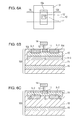
Hereinafter, an example of a manufacturing method of the imaging apparatus of the present embodiment will be explained. FIGS. 4A-4C are diagrams used to explain the manufacturing method of the imaging apparatus of the present embodiment. Each of FIGS. 4A-4C schematically illustrates a cross sectional structure along a line A-B in FIG. 1. Elements of FIGS. 4A-4C corresponding to those illustrated in any of FIGS. 1 through 3B are designated by the same reference numerals as FIGS. 1 through 3B.
In a step illustrated in FIG. 4A, the gate region 9 of the JFET is formed. In this step, a first mask 17 which defines a first opening 209 is used. The first mask 17 is, for example, obtained by patterning a photoresist by photolithography method.
Impurities to be acceptors, such as boron, are doped into the semiconductor substrate 100 through the first opening 209, whereby the gate region 9 is formed in a region corresponding to the first opening 209. For example, the gate region 9 may be formed by an ion implantation using the first mask 17. By performing a plurality of ion implantations at different implantation energies, the surface gate region 9-1 and the buried gate region 9-2 may be formed at different depths from each other. Generally, a higher energy is used to form a semiconductor region at a deeper position in the semiconductor substrate 100. According to the implantation energies, the surface gate region 9-1 and the buried gate region 9-2 may be formed in spatially continuously by an impurity diffusion along a vertical direction to the surface SR. After forming the gate region 9, the first mask 17 is removed.
Besides the ion implantation, a thermal diffusion method may be used to dope the semiconductor substrate 100 with the impurity.
In a step illustrated in FIG. 4B, the channel region 10 of the JFET is formed. In this step, a second mask 18 which defines a second opening 210 is used. The second mask 18 is, for example, obtained by patterning a photoresist by photolithography method.
Impurities to be donors, such as phosphorus and arsenic, are doped into the semiconductor substrate 100 through the second opening 210, whereby the channel region 10 is formed in a region corresponding to the second opening 210. For example, the channel region 10 may be formed by an ion implantation using the second mask 18. The implantation energy used to form the channel region 10 may be adjusted so that the channel region 10 is formed at a depth between the surface gate region 9-1 and the buried gate region 9-2. After forming the channel region 10, the second mask 18 is removed.
Although it is not shown in FIG. 4, a P-type semiconductor region that electrically connects the plurality of the gate regions 9 to each other may be formed using a third mask 19 which defines third openings 203 and 207. The third mask 19 is, for example, obtained by patterning a photoresist by photolithography method.
In the present embodiment, the FD region 3 and the source region 7 of the reset MOS transistor are formed using the third mask 19. These regions electrically connect the gate regions 9 to each other. After forming the P-type semiconductor region that electrically connects the plurality of the gate regions 9 to each other, the third mask 19 is removed.
In a step illustrated in FIG. 4C, the source region 11 which is connected to the source-side portion 10 s of the channel region 10 is formed. In this step, a mask 20 which defines an opening 211 is used. The mask 20 is a hard mask. The mask 20 includes an insulator film made of an inorganic material such as silicon oxide, silicon nitride, and silicon oxy-nitride.
Impurities to be donors, such as phosphorus and arsenic, are doped into the semiconductor substrate 100 through the opening 211, whereby the source region 11 is formed in a region corresponding to the opening 211.
The mask 20 may be used as an interlayer insulation film, when the hard mask is used as the mask 20 as mentioned above. Specifically, after forming the source region 11, the mask 20 remains not to be removed, and then, the contact plug 12 electrically connected to the source region 11 is formed in the opening 211. Thereafter, the output line 14 connected to the contact plug 12 is formed on the mask 20.
Next, planar structures of the first through third masks 17-19 and relative positions thereof will be explained. FIGS. 5A and 5B are diagrams schematically illustrating the first through third masks 17-19 used in the steps illustrated in FIGS. 4A-4C. Elements of FIGS. 5A-5B corresponding to those illustrated in any of FIGS. 4A through 4C are designated by the same reference numerals as FIGS. 4A through 4C.
Each of FIGS. 5A and 5B illustrates the first opening 209, the second opening 210 and the third openings 203 and 207. FIG. 5B distinguishes each part of the second opening 210. In the present embodiment, each of the first opening 209, the second opening 210 and the third openings 203 and 207 has a rectangular shape. The first mask 17 which defines the first opening 209 is indicated as an area outside a rectangle indicating the opening 209. The second mask 18 which defines the second opening 210 is indicated as an area outside a rectangle indicating the second opening 210. The third mask 19 which defines the third openings 203 and 207 is indicated as an area outside a rectangle indicating the third openings 203 and 207.
For ease of explanation, the first through third openings 209, 210, 203 and 207 are illustrated to overlap with each other in FIGS. 5A and 5B, whereby indicates alignments between the masks. However, the mask may be removed after forming the corresponding semiconductor region in each step. Accordingly, two or more masks are not necessarily provided at the same time.
The first opening 209 and the second opening 210 intersect each other when viewed in a planar view. In other words, an orthogonal projection of the first opening 209 onto a plane parallel to the surface of the semiconductor substrate 100 intersect an orthogonal projection of the second opening 210 onto the plane.
As illustrated in FIG. 5B, the second opening 210 includes a source-side portion 210 s and a drain-side portion 210 d. The source-side portion 210 s of the second opening 210 corresponds to the source-side portion 10 s of the channel region 10. The drain-side portion 210 d of the opening 210 corresponds to the drain-side portion 10 d of the channel region 10. In FIG. 5B, there are two drain-side portions 210 d: one is a part on left side of the first opening 209L, the other is a part on right side of the first opening 209R.
Each of the source-side portion 210 s and the drain-side portion 210 d of the second opening 210 overlaps with the first mask 17 when viewed in a planar view. In other words, each of an orthogonal projection of the source-side portion 210 s onto a plane parallel to the surface of the semiconductor substrate 100 and an orthogonal projection of the drain-side portion 210 d onto the plane overlaps with an orthogonal projection of the first mask 17 onto the plane. Accordingly, as illustrated in FIG. 5, the channel length of the JFET is defined by the ends of the first opening 209. The channel width of the JFET is defined by the ends of the second opening 210.
According to the above described configuration, even though there could be alignment errors between the first mask 17 used to form the gate region 9 and the second mask 18 used to form the channel region 10, a shape of the channel of the JFET is almost steady, or constant, or unchanged. Thus, fluctuations in the channel length and the channel width of the JFET may be reduced. As a result, fluctuations in the characteristic of the JFET may be reduced.
In the present embodiment, the first opening includes a plurality of openings 209L and 209R which are divided by the first mask 17. Each of the openings 209L and 209R intersects the second opening 210 when viewed in a planar view. In other words, each of orthogonal projections of the plurality of the opening 209L and 209R onto a plane parallel to the surface of the semiconductor substrate 100 intersects the orthogonal projection of the second opening 210. The source-side portion 210 s of the second opening 210 overlaps with the first mask 17, specifically, with a part of the first mask 17 which is arranged, located, positioned, or disposed between the two openings 209L and 209R, when viewed in a planar view.
The first opening 209 partially overlap with the third openings 203 and 207 when viewed in a planar view. In other words, the orthogonal projection of the first opening 209 onto a plane parallel to the surface of the semiconductor substrate 100 partially overlaps with the orthogonal projections of the third openings 203 and 207 onto the plane.
According to the above described configuration, the effective channel width of the JFET may be widened. That is to say, the drive capability of the JFET may be improved. Thus, the imaging apparatus may operate at a high speed.
The entirety of the second opening 210 is overlapped with the third mask 19 when viewed in a planar view. In this configuration, it is possible to reduce amount of impurities doped into the channel region 10 when doping the semiconductor substrate 100 with impurities using the third mask 19. Accordingly, even though the P-type semiconductor region that electrically connects the gate regions 9 is formed, fluctuations in the electrical characteristic of the JFET may be reduced.
Here, a variation of the present embodiment will be explained. FIG. 6A is a diagram schematically illustrating a planar structure of an imaging apparatus of the present embodiment. A JFET is illustrated in FIG. 6A. Elements of FIG. 6A corresponding to those illustrated in FIG. 1 are designated by the same reference numerals as FIG. 1. The structure of the imaging apparatus is similar to the first embodiment except for those explained otherwise.
One of the features of the present embodiment is a shape of a gate region 61 of the JFET. Specifically, the gate region 61 surrounds the source-side portion 10 s of the channel region 10 when viewed in a planar view. Two parts of the gate region 61 respectively intersect the channel region 10 when viewed in a planar view. Each of the source-side region 10 s and the drain-side region 10 d of the channel region 10 does not overlap with the gate region 61. Each of the source-side region 10 s and the drain-side region 10 d protrudes out of the gate region 61. Accordingly, the channel length of the JFET is defined by the end of the gate region 61. The channel width of the JFET is defined by the end of the channel region 10.
According to the above described configuration, even though there could be alignment errors between a mask used to form the gate region 61 and a mask used to form the channel region 10, a shape of the channel of the JFET is almost steady, or constant, or unchanged. Thus, fluctuations in the channel length and the channel width of the JFET may be reduced. As a result, fluctuations in the characteristic of the JFET may be reduced.
In the variation illustrated in FIG. 6A, the gate region 61 is spatially continuous. The surface gate region and the buried gate region is electrically connected to each other via a connecting portion which does not overlap with the channel region 10 when viewed in a planar view. Thus, the effective channel width of the JFET may be widened while omitting the step to form the semiconductor region having the same conductivity type as the two gate regions and connecting the two gate regions. For example, a step to form the FD region 3 shown in FIG. 1 may be omitted.
Here, another variation will be explained. FIG. 6B is a diagram schematically illustrating a cross sectional structure of an imaging apparatus of the present embodiment. A JFET is illustrated in FIG. 6B. Elements of FIG. 6B corresponding to those illustrated in FIG. 1 are designated by the same reference numerals as FIG. 1. The structure of the imaging apparatus is similar to the first embodiment except for those explained otherwise.
In the JFET illustrated in FIG. 6B, the gate region 9 includes a surface gate region 9-1 and a buried gate region 9-3. The buried gate region 9-3 includes a P-type semiconductor region having, in a planar view, a different shape from that of the surface gate region 9-1. The buried gate region 9-3 is electrically connected to the surface gate region 9-1. In FIG. 6B, the planar shape of the buried gate region 9-3 is identical to the planar shape of the channel region 10. Or, the buried gate region 9-3 may contain completely the channel region 10 when viewed in a planar view.
Here, another variation will be explained. FIG. 6C is a diagram schematically illustrating a cross sectional structure of an imaging apparatus of the present embodiment. A JFET is illustrated in FIG. 6C. Elements of FIG. 6C corresponding to those illustrated in FIG. 1 are designated by the same reference numerals as FIG. 1. The structure of the imaging apparatus is similar to the first embodiment except for those explained otherwise. The gate region 9 of the JFET illustrated in FIG. 6C only includes the buried gate region 9-2.
In these variations, the gate region 9 and the channel region 10 intersect each other. Accordingly, fluctuation of the electrical characteristic of the JFET may be reduced.
As described above, according to some of the embodiments, fluctuations of the characteristic of the JFET may be reduced.
Second Embodiment
Now, another embodiment will be described. Difference with the first embodiment is that a structure to reduce a parasitic JFET current is provided under the source region of the JFET. The explanation will focus on the differences with the first embodiment, and the explanation on the same structure as the first embodiment will be omitted.
FIG. 7 is a diagram schematically illustrating a planar structure of an imaging apparatus of the present embodiment. A JFET is illustrated in FIG. 7. Elements of FIG. 7 corresponding to those illustrated in FIG. 1 are designated by the same reference numerals as FIG. 1.
The pixel of the present embodiment includes a P-type semiconductor region 21. The semiconductor region 21 overlaps with the source region 11 when viewed in a planar view. In other words, an orthogonal projection of the P-type semiconductor region 21 onto a plane parallel to the surface of the semiconductor substrate overlaps with an orthogonal projection of the source region 11 onto the plane. The p-type semiconductor region 21 is arranged, located, positioned, or disposed between the two gate regions 9 when viewed in a planar view. In other words, the orthogonal projection of the P-type semiconductor region 21 onto the plane parallel to the surface of the semiconductor substrate is located between the orthogonal projections of the two gate regions 9 onto the plane.
FIG. 8A is a diagram schematically illustrating a cross sectional structure of the imaging apparatus of the present embodiment. FIG. 8A schematically illustrates the cross sectional structure along a line G-H in FIG. 7. Elements of FIG. 8A corresponding to those illustrated in any of FIGS. 1 through 7 are designated by the same reference numerals as FIGS. 1 through 7.
As illustrated in FIG. 8A, the P-type semiconductor region 21 is arranged, located, positioned, or disposed at a deeper position than the channel region 10. When the P-type semiconductor region 21 and the channel region 10 are formed by ion implantations, a peak in an impurity density profile along a depth direction of the P-type semiconductor region 21 is located at a deeper position than a peek in an impurity density profile along the depth direction of the channel region 10. The depth direction is defined as a vertical direction to the surface SR.
In the present embodiment, the entirety of the P-type semiconductor region 21 is arranged, located, positioned, or disposed at the same depth as the buried gate region 9-2. In FIG. 8A, the P-type semiconductor region 21 and the buried gate region 9-2 are electrically connected to each other. The P-type semiconductor region 21 and the buried gate region 9-2 may be formed spatially continuously.
FIG. 8B is a diagram schematically illustrating a cross sectional structure of the imaging apparatus of the present embodiment. FIG. 8B schematically illustrates the cross sectional structure along a line I-J in FIG. 7. Elements of FIG. 8B corresponding to those illustrated in any of FIGS. 1 through 7 are designated by the same reference numerals as FIGS. 1 through 7.
As illustrated in FIG. 8B, the P-type semiconductor region 21 is wider than the channel region 10 in the channel width direction. In the present embodiment, P-type semiconductor region 21 extends to the extent that the P-type semiconductor region 21 reaches a region directly under the FD region 3 and a region directly under the source region 7 of the reset MOS transistor.
The cross sectional structure along a line K-L in FIG. 7 is the same as those of the first embodiment. That is to say, FIG. 3B schematically illustrates the cross sectional structure of the present embodiment.
According to the above described configuration, electrical resistance between the channel region 10 and the N-type semiconductor region 15 may be high. As a result, it is possible to reduce a parasitic current which runs through a region other than the channel defined by the gate region 9 and the channel region 10. Since the dependency of the parasitic current on the gate voltage is low, a large parasitic current may deteriorate the current-voltage characteristic of the JFET. Thus, reducing the parasitic current may improve the current-voltage characteristic of the JFET.
An impurity density of the P-type semiconductor region 21 may be lower than that of the buried gate region 9-2. In this configuration, even though there could be alignment error when forming the P-type semiconductor region 21, fluctuations in the electrical characteristic of the JFET may be reduced.
A manufacturing method of the imaging apparatus of the present embodiment further includes a step to form the P-type semiconductor region 21 in addition to the method explained in the first embodiment. The P-type semiconductor region 21, for example, may be formed by using a mask illustrated in FIG. 7.
As described above, according to the present embodiment, the parasitic JFET current may be reduced in addition to obtaining technical effect of the first embodiment.
Third Embodiment
Now, another embodiment will be described. Difference with the first embodiment or the second embodiment is that the JFET includes an LDD structure. The explanation will focus on the differences with the first and/or embodiments, and the explanation on the same structure as the first and/or second embodiments will be omitted.
A planar structure of an imaging apparatus of the present embodiment is the same as the first or second embodiment. That is to say, FIG. 1 or FIG. 7 schematically illustrates the planar structure of the imaging apparatus of the present embodiment. In the present embodiment, an N-type semiconductor region is added to a region which overlaps with the gate regions of FIG. 1 or FIG. 7.
FIGS. 9A-9C are diagrams used to explain a manufacturing method of the imaging apparatus of the present embodiment. Each of FIGS. 9A-9C schematically illustrates a cross sectional structure along a line A-B in FIG. 1, which is a cross section including the channel length direction of the JFET. The P-type semiconductor region 21 may be added into the structure illustrated in FIGS. 9A-9C.
In a step illustrated in FIG. 9A, the surface gate region 9-1 and the buried gate region 9-2 are formed. A forming method of the surface gate region 9-1 and the buried gate region 9-2 is the same as those illustrated in FIG. 4A of the first embodiment. As described in the explanation of the first embodiment, the first mask 17 which defines the first opening 209 is used in this step.
In the present embodiment, an N-type semiconductor region 22 is formed using the first mask 17 which has been used or is to be used to form the surface gate region 9-1 and the buried gate region 9-2. Impurities to be donors, such as phosphorus and arsenic, are doped into the semiconductor substrate 100 through the first opening 209, whereby the N-type semiconductor region 22 is formed in a region corresponding to the first opening 209.
The first mask 17 is, for example, obtained by patterning a photoresist by photolithography method. Otherwise, the first mask 17 may be a hard mask.
The N-type semiconductor region 22 overlaps with the gate region 9 when viewed in a planar view. In other words, an orthogonal projection of the N-type semiconductor region 22 onto a plane parallel to the surface of the semiconductor substrate 100 is identical to the orthogonal projection of the gate region 9 onto the plane. The N-type semiconductor region 22 is arranged, located, positioned, or disposed at a depth between the surface gate region 9-1 and the buried gate region 9-2. The surface gate region 9-1, the buried gate region 9-2 and the N-type semiconductor region 22 may be formed by ion implantations. In that case, the implantation energies used to form the surface gate region 9-1, the buried gate region 9-2 and the N-type semiconductor region 22 may be adjusted so that the N-type semiconductor region 22 is arranged, located, positioned, or disposed at the depth between the surface gate region 9-1 and the buried gate region 9-2.
In a step illustrated in FIG. 9B, the channel region 10 of the JFET is formed. Since the step to form the channel region 10 is the same as those in the first embodiment, the explanation in detail will be omitted here.
In a step illustrated in FIG. 9C, the source region 11 is formed. Since the step to form the source region 11 is the same as those in the first embodiment, the explanation in detail will be omitted here.
A part, which has not been doped with impurities in the step illustrated in FIG. 9A, of the channel region 10 functions as a potential grading region (or, electric-field alleviation region). The channel is formed in a region where the channel region 10 and the N-type semiconductor region 22 overlap with each other. Impurities are doped into the region during each of the two steps of forming the channel region 10 and of forming the N-type semiconductor region 22. Accordingly, the other part of the channel region, i.e. the part which has not been doped with impurities in the step illustrated in FIG. 9A has a relatively low impurity density. Thus, it is possible to decrease an impurity density of a part of the channel region 10, which protrudes out of the gate region 9.
According to the low impurity density drain, an electric field near the drain of the JFET may be alleviated. If a large electric field is generated in the vicinity of the drain of the JFET, the channel current causes impact-ionization, and thus, generates carriers. The generated carriers may run into the gate region 9 that accumulates signal carriers, whereby noise may be generated. The alleviation of the electrical field around the drain of the JFET may prevent the impact-ionization which causes a noise. As a result, noises in the pixel may be reduced.
Generally, the channel current of the JFET causes the impact-ionization in a pinch-off region near the drain region. To alleviate the electrical field of the pinch-off region and prevent the impact-ionization, a low impurity density of the drain region may be used.
In the present embodiment, the channel of the JFET may be formed by only the N-type semiconductor region 22 without forming the channel region 10. In this case, a part of the N-type semiconductor region 15 forms the drain region. Without the channel region 10, the channel width of the JFET is defined as a distance between the FD region 3 and the source region 7 of the reset MOS transistor along the channel width direction.
As described above, according to the present embodiment, noises may be reduced in addition to obtaining technical effect of the first embodiment.
Fourth Embodiment
An imaging system according to an embodiment of the present disclosure will be described. Examples of the imaging system include digital still cameras, digital camcorders, copiers, facsimiles, mobile phones, in-vehicle cameras, and orbiting satellites. FIG. 10 illustrates a block diagram of a digital still camera serving as an example of the imaging system.
In FIG. 10, a reference numeral 1001 denotes a barrier for lens protection, 1002 denotes a lens causing the imaging apparatus 1004 to perform focusing on an optical image of a photographic subject, and 1003 denotes a diaphragm configured to change the amount of light passing through the lens 1002. A reference numeral 1004 denotes an imaging apparatus described in the above embodiments, and is configured to convert the optical image formed by the lens 1002 as image data. Now, let us say that an analog-to-digital (AD) conversion unit is formed on a semiconductor substrate of the imaging apparatus 1004. A reference numeral 1007 denotes a signal processor configured to subject imaged data output by the imaging apparatus 1004 to various types of correction or to compress the imaged data. In FIG. 10, a reference numeral 1008 denotes a timing generator configured to output various types of timing signals to the imaging apparatus 1004 and signal processor 1007, and 1009 denotes an overall control unit configured to control the entire digital still camera. A reference numeral 1010 denotes a frame memory unit configured to temporarily store image data, 1011 denotes an interface unit configured to perform recording or readout on a recording medium, and 1012 denotes a recoding medium capable of connecting to and disconnecting from the imaging apparatus 1004, such as semiconductor memory or the like, configured to preform recording or readout of imaged data. Also, a reference numeral 1013 denotes an interface unit configured to communicate with an external computer or the like. Here, a timing signal or the like may be input from the outside of the imaging system. The imaging system has to include at least the imaging apparatus 1004, and the signal processor 1007 configured to process the imaged signal output from the imaging apparatus 1004.
A configuration has been described in the present embodiment wherein the imaging apparatus 1004 and AD conversion unit are provided to a different semiconductor substrate. However, the imaging apparatus 1004 and AD conversion unit may be formed on the same semiconductor substrate. Also, the imaging apparatus 1004 and signal processor 1007 may be formed on the same semiconductor substrate.
Also, the signal processor 1007 may be configured to process a signal based on an electric carrier generated at the first photoelectric conversion unit, and a signal based on an electric carrier generated at the second photoelectric conversion unit to obtain distance information from the imaging apparatus 1004 to a subject.
The imaging apparatus according to one of the first embodiment through the third embodiment is employed as the imaging apparatus 1004 in the imaging system according to the present embodiment. Thus, fluctuations of the characteristic of the JFET may be reduced by applying an embodiment of the present disclosure to an imaging system.
While the present disclosure has been described with reference to exemplary embodiments, it is to be understood that the invention is not limited to the disclosed exemplary embodiments. The scope of the following claims is to be accorded the broadest interpretation so as to encompass all such modifications and equivalent structures and functions.
This application claims the benefit of PCT/JP2013/084566, filed Dec. 25, 2013, which is hereby incorporated by reference herein in its entirety.

Claims (8)

What is claimed is:
1. An imaging apparatus comprising:
a plurality of pixels, each pixel including a junction type field effect transistor provided in a semiconductor substrate,
wherein
the junction type field effect transistor includes a gate region and a channel region,
an orthogonal projection of the gate region onto a plane parallel to a surface of the semiconductor substrate intersects an orthogonal projection of the channel region onto the plane,
a length of the orthogonal projection of the channel region in a channel length direction is greater than a total length of the orthogonal projection of the gate region in the channel length direction, and
each of a source-side portion of the orthogonal projection of the channel region and a drain-side portion of the orthogonal projection of the channel region protrudes out of the orthogonal projection of the gate region,
each of first and second parts of the orthogonal projection of the gate region protrudes out of a periphery of the orthogonal projection of the channel region in a channel width direction toward opposite directions to each other;
the gate region includes a surface gate region in a surface side of the semiconductor substrate and a buried gate region disposed at different depths from each other,
the channel region is disposed between the surface gate region and the buried gate region, and
an orthogonal projection of the surface gate region onto the plane is identical to an orthogonal projection of the buried gate region onto the plane.
2. The imaging apparatus according to claim 1, wherein
the gate region includes a plurality of sub-regions which are disposed to sandwich a source region of the junction type field effect transistor and are electrically connected to each other,
each of orthogonal projections of the sub-regions onto the plane intersects the orthogonal projection of the channel region.
3. The imaging apparatus according to claim 1, wherein
a periphery of the orthogonal projection of the gate region includes two lines parallel to each other, and
a periphery of the orthogonal projection of the channel region includes two lines parallel to each other.
4. An imaging system comprising:
the imaging apparatus according to claim 1; and
a signal processing unit configured to process a signal output from the imaging apparatus.
5. An imaging apparatus comprising:
a plurality of pixels, each pixel including a junction type field effect transistor provided in a semiconductor substrate,
wherein
the junction type field effect transistor includes a surface gate region in a surface of the semiconductor substrate, a buried gate region and a channel region, disposed at different depths from each other,
the channel region is disposed between the surface gate region and the buried gate region,
each of an orthogonal projection of the surface gate region onto a plane parallel to a surface of the semiconductor substrate and an orthogonal projection of the buried gate region onto the plane intersects an orthogonal projection of the channel region onto the plane,
a length of the orthogonal projection of the channel region in a channel length direction is greater than a total length of the orthogonal projection of the surface gate region in the channel length direction and greater than a total length of the orthogonal projection of the buried gate region in the channel length direction,
each of first and second parts of the orthogonal projection of the surface gate region protrudes out of a periphery of the orthogonal projection of the channel region in a channel width direction toward opposite directions to each other, and
each of first and second parts of the orthogonal projection of the buried gate region protrudes out of the periphery of the orthogonal projection of the channel region in a channel width direction toward opposite directions to each other.
6. The imaging apparatus according to claim 5, wherein
the surface gate region includes a plurality of sub-regions which are disposed to sandwich a source region of the junction type field effect transistor and are electrically connected to each other,
each of orthogonal projections of the sub-regions onto the plane intersects the orthogonal projection of the channel region.
7. The imaging apparatus according to claim 5, wherein
the buried gate region includes a plurality of sub-regions which are disposed to sandwich a source region of the junction type field effect transistor and are electrically connected to each other,
each of orthogonal projections of the sub-regions onto the plane intersects the orthogonal projection of the channel region.
8. An imaging system comprising:
the imaging apparatus according to claim 5; and
a signal processing unit configured to process a signal output from the imaging apparatus.
US14/576,028 2013-12-25 2014-12-18 Imaging apparatus, imaging system and manufacturing method of imaging apparatus Expired - Fee Related US9577004B2 (en)

Applications Claiming Priority (2)

Application Number Priority Date Filing Date Title
PCT/JP2013/084566 WO2015097771A1 (en) 2013-12-25 2013-12-25 Image pickup apparatus, image pickup system, and image pickup apparatus manufacturing method
JPPCT/JP2013/084566 2013-12-25

Publications (2)

Publication Number Publication Date
US20150179688A1 US20150179688A1 (en) 2015-06-25
US9577004B2 true US9577004B2 (en) 2017-02-21

Family

ID=53400937

Family Applications (1)

Application Number Title Priority Date Filing Date
US14/576,028 Expired - Fee Related US9577004B2 (en) 2013-12-25 2014-12-18 Imaging apparatus, imaging system and manufacturing method of imaging apparatus

Country Status (7)

Country Link
US (1) US9577004B2 (en)
EP (1) EP3091576A4 (en)
JP (1) JP6227010B2 (en)
KR (1) KR101866673B1 (en)
CN (1) CN105830219B (en)
RU (1) RU2638108C1 (en)
WO (1) WO2015097771A1 (en)

Families Citing this family (2)

* Cited by examiner, † Cited by third party
Publication number Priority date Publication date Assignee Title
US9653618B1 (en) * 2015-10-21 2017-05-16 United Silicon Carbide, Inc. Planar triple-implanted JFET
US10446695B2 (en) 2015-10-21 2019-10-15 United Silicone Carbide, Inc. Planar multi-implanted JFET

Citations (8)

* Cited by examiner, † Cited by third party
Publication number Priority date Publication date Assignee Title
US4686555A (en) * 1982-12-14 1987-08-11 Olympus Optical Co., Ltd. Solid state image sensor
US5089862A (en) * 1986-05-12 1992-02-18 Warner Jr Raymond M Monocrystalline three-dimensional integrated circuit
US20050093017A1 (en) * 2002-03-15 2005-05-05 Kazuhiro Fujikawa Lateral junctiion field-effect transistor and its manufacturing method
US20050173726A1 (en) * 2004-02-09 2005-08-11 International Rectifier Corp. Normally off JFET
JP2006196789A (en) 2005-01-14 2006-07-27 Nikon Corp Junction field effect transistor, manufacturing method thereof, and solid-state imaging element
JP2007165736A (en) 2005-12-16 2007-06-28 Nikon Corp Jfet (junction type field effect transistor) and solid-state image pickup device using same
US20080093635A1 (en) * 2006-10-23 2008-04-24 Sanyo Electric Co., Ltd. Junction Fet and Method of Manufacturing the Same
US20080272414A1 (en) * 2007-05-01 2008-11-06 Dsm Solutions, Inc. Image sensing cell, device, method of operation, and method of manufacture

Family Cites Families (14)

* Cited by examiner, † Cited by third party
Publication number Priority date Publication date Assignee Title
JPS5664470A (en) * 1979-10-31 1981-06-01 Pioneer Electronic Corp Junction type field-effect transistor
JPS5941871A (en) * 1982-08-31 1984-03-08 Matsushita Electronics Corp Junction type field effect semiconductor device
JP3109274B2 (en) * 1992-08-31 2000-11-13 日本電気株式会社 Semiconductor device and manufacturing method thereof
JP2002231730A (en) * 2001-02-01 2002-08-16 Sumitomo Electric Ind Ltd Lateral junction field-effect transistor and method of manufacturing the same
JP3812421B2 (en) * 2001-06-14 2006-08-23 住友電気工業株式会社 Horizontal junction field effect transistor
JP2005252083A (en) * 2004-03-05 2005-09-15 Nikon Corp Junction field effect transistor and solid state imaging device
JP2006179825A (en) * 2004-12-24 2006-07-06 Nikon Corp Amplifying solid-state imaging device
JP2006351729A (en) * 2005-06-14 2006-12-28 Canon Inc Junction type field effect transistor, manufacturing method thereof, and solid-state imaging apparatus
KR100776146B1 (en) * 2006-05-04 2007-11-15 매그나칩 반도체 유한회사 Cmos image sensor with improved performance incorporating pixels with burst reset operation
KR100851495B1 (en) * 2007-05-14 2008-08-08 매그나칩 반도체 유한회사 Small pixel for image sensors with jfet and vertically integrated reset diodes
JP2009043923A (en) * 2007-08-08 2009-02-26 Sanyo Electric Co Ltd Semiconductor device, and manufacturing method of the same
JP4759590B2 (en) * 2008-05-09 2011-08-31 キヤノン株式会社 Photoelectric conversion device and imaging system using the same
JP5495524B2 (en) * 2008-08-18 2014-05-21 キヤノン株式会社 Photoelectric conversion device
CN202633312U (en) * 2012-01-11 2012-12-26 格科微电子(上海)有限公司 Image sensor and source follower

Patent Citations (8)

* Cited by examiner, † Cited by third party
Publication number Priority date Publication date Assignee Title
US4686555A (en) * 1982-12-14 1987-08-11 Olympus Optical Co., Ltd. Solid state image sensor
US5089862A (en) * 1986-05-12 1992-02-18 Warner Jr Raymond M Monocrystalline three-dimensional integrated circuit
US20050093017A1 (en) * 2002-03-15 2005-05-05 Kazuhiro Fujikawa Lateral junctiion field-effect transistor and its manufacturing method
US20050173726A1 (en) * 2004-02-09 2005-08-11 International Rectifier Corp. Normally off JFET
JP2006196789A (en) 2005-01-14 2006-07-27 Nikon Corp Junction field effect transistor, manufacturing method thereof, and solid-state imaging element
JP2007165736A (en) 2005-12-16 2007-06-28 Nikon Corp Jfet (junction type field effect transistor) and solid-state image pickup device using same
US20080093635A1 (en) * 2006-10-23 2008-04-24 Sanyo Electric Co., Ltd. Junction Fet and Method of Manufacturing the Same
US20080272414A1 (en) * 2007-05-01 2008-11-06 Dsm Solutions, Inc. Image sensing cell, device, method of operation, and method of manufacture

Also Published As

Publication number Publication date
KR101866673B1 (en) 2018-06-11
WO2015097771A1 (en) 2015-07-02
WO2015097771A9 (en) 2016-01-07
EP3091576A1 (en) 2016-11-09
US20150179688A1 (en) 2015-06-25
CN105830219A (en) 2016-08-03
JP6227010B2 (en) 2017-11-08
EP3091576A4 (en) 2017-11-29
RU2638108C1 (en) 2017-12-11
CN105830219B (en) 2019-01-01
KR20160100354A (en) 2016-08-23
JPWO2015097771A1 (en) 2017-03-23

Similar Documents

Publication Publication Date Title
US8779544B2 (en) Photoelectric conversion apparatus and imaging system having revision with multiple impurity densities
US7709869B2 (en) Photoelectric conversion device, method of manufacturing the same, and image sensing system
US10217780B2 (en) Solid-state imaging apparatus, method for manufacturing the same, and imaging system
JP5814626B2 (en) Photoelectric conversion device and method of manufacturing photoelectric conversion device
US9466641B2 (en) Solid-state imaging device
KR20110132517A (en) Method for production of solid-state imaging element, solid-state imaging element, and imaging apparatus
US11695029B2 (en) Pixel formation method
KR101997539B1 (en) Image sensor and method of forming the same
US9577004B2 (en) Imaging apparatus, imaging system and manufacturing method of imaging apparatus
US9391116B2 (en) Imaging apparatus, imaging system and manufacturing method of imaging apparatus
US9793314B2 (en) Imaging apparatus, imaging system and manufacturing method of imaging apparatus
JP2017220603A (en) Solid state imaging device and manufacturing method of solid state imaging device
JP2002353431A (en) Photoelectric transducer and manufacturing method therefor
US9171880B2 (en) Photoelectric conversion device, method of manufacturing the same, and camera
JP6066616B2 (en) Imaging apparatus and imaging system
JP2009302448A (en) Manufacturing method of solid-state imaging element
JP2005209674A (en) Charge transfer device, method of manufacturing the same and solid state imaging device
JP2007299806A (en) Solid-state image pickup device and manufacturing method thereof
JP2014060258A (en) Solid state image pickup element and manufacturing method of the same, and electronic information instrument
JP2013004581A (en) Solid state image pickup device and method of manufacturing the same

Legal Events

Date Code Title Description
AS Assignment

Owner name: CANON KABUSHIKI KAISHA, JAPAN

Free format text: ASSIGNMENT OF ASSIGNORS INTEREST;ASSIGNORS:SHINOHARA, MAHITO;KOBAYASHI, MASAHIRO;ITAHASHI, MASATSUGU;REEL/FRAME:035798/0829

Effective date: 20141202

STCF Information on status: patent grant

Free format text: PATENTED CASE

FEPP Fee payment procedure

Free format text: MAINTENANCE FEE REMINDER MAILED (ORIGINAL EVENT CODE: REM.); ENTITY STATUS OF PATENT OWNER: LARGE ENTITY

LAPS Lapse for failure to pay maintenance fees

Free format text: PATENT EXPIRED FOR FAILURE TO PAY MAINTENANCE FEES (ORIGINAL EVENT CODE: EXP.); ENTITY STATUS OF PATENT OWNER: LARGE ENTITY

STCH Information on status: patent discontinuation

Free format text: PATENT EXPIRED DUE TO NONPAYMENT OF MAINTENANCE FEES UNDER 37 CFR 1.362

FP Lapsed due to failure to pay maintenance fee

Effective date: 20210221