JP6154392B2 - 発光ダイオードおよび発光ダイオードを有する照明装置 - Google Patents
発光ダイオードおよび発光ダイオードを有する照明装置 Download PDFInfo
- Publication number
- JP6154392B2 JP6154392B2 JP2014539175A JP2014539175A JP6154392B2 JP 6154392 B2 JP6154392 B2 JP 6154392B2 JP 2014539175 A JP2014539175 A JP 2014539175A JP 2014539175 A JP2014539175 A JP 2014539175A JP 6154392 B2 JP6154392 B2 JP 6154392B2
- Authority
- JP
- Japan
- Prior art keywords
- light
- vertical surface
- cover
- light emitting
- transmission member
- Prior art date
- Legal status (The legal status is an assumption and is not a legal conclusion. Google has not performed a legal analysis and makes no representation as to the accuracy of the status listed.)
- Expired - Fee Related
Links
- 230000005540 biological transmission Effects 0.000 claims description 93
- 239000000758 substrate Substances 0.000 claims description 25
- OAICVXFJPJFONN-UHFFFAOYSA-N Phosphorus Chemical compound [P] OAICVXFJPJFONN-UHFFFAOYSA-N 0.000 claims description 15
- 238000009792 diffusion process Methods 0.000 claims description 7
- 239000011347 resin Substances 0.000 description 6
- 229920005989 resin Polymers 0.000 description 6
- 238000005286 illumination Methods 0.000 description 4
- 239000002245 particle Substances 0.000 description 3
- VYPSYNLAJGMNEJ-UHFFFAOYSA-N Silicium dioxide Chemical compound O=[Si]=O VYPSYNLAJGMNEJ-UHFFFAOYSA-N 0.000 description 2
- 230000002093 peripheral effect Effects 0.000 description 2
- 238000007789 sealing Methods 0.000 description 2
- 239000004593 Epoxy Substances 0.000 description 1
- 229910004298 SiO 2 Inorganic materials 0.000 description 1
- GWEVSGVZZGPLCZ-UHFFFAOYSA-N Titan oxide Chemical compound O=[Ti]=O GWEVSGVZZGPLCZ-UHFFFAOYSA-N 0.000 description 1
- PNEYBMLMFCGWSK-UHFFFAOYSA-N aluminium oxide Inorganic materials [O-2].[O-2].[O-2].[Al+3].[Al+3] PNEYBMLMFCGWSK-UHFFFAOYSA-N 0.000 description 1
- 239000003086 colorant Substances 0.000 description 1
- 239000011521 glass Substances 0.000 description 1
- 229910052751 metal Inorganic materials 0.000 description 1
- 239000002184 metal Substances 0.000 description 1
- 238000012986 modification Methods 0.000 description 1
- 230000004048 modification Effects 0.000 description 1
- 230000005855 radiation Effects 0.000 description 1
- 235000012239 silicon dioxide Nutrition 0.000 description 1
- 239000000377 silicon dioxide Substances 0.000 description 1
Images

Classifications
-
- H—ELECTRICITY
- H10—SEMICONDUCTOR DEVICES; ELECTRIC SOLID-STATE DEVICES NOT OTHERWISE PROVIDED FOR
- H10H—INORGANIC LIGHT-EMITTING SEMICONDUCTOR DEVICES HAVING POTENTIAL BARRIERS
- H10H20/00—Individual inorganic light-emitting semiconductor devices having potential barriers, e.g. light-emitting diodes [LED]
- H10H20/80—Constructional details
- H10H20/85—Packages
- H10H20/851—Wavelength conversion means
- H10H20/8515—Wavelength conversion means not being in contact with the bodies
-
- H—ELECTRICITY
- H10—SEMICONDUCTOR DEVICES; ELECTRIC SOLID-STATE DEVICES NOT OTHERWISE PROVIDED FOR
- H10H—INORGANIC LIGHT-EMITTING SEMICONDUCTOR DEVICES HAVING POTENTIAL BARRIERS
- H10H20/00—Individual inorganic light-emitting semiconductor devices having potential barriers, e.g. light-emitting diodes [LED]
- H10H20/80—Constructional details
- H10H20/85—Packages
- H10H20/851—Wavelength conversion means
- H10H20/8514—Wavelength conversion means characterised by their shape, e.g. plate or foil
-
- H—ELECTRICITY
- H10—SEMICONDUCTOR DEVICES; ELECTRIC SOLID-STATE DEVICES NOT OTHERWISE PROVIDED FOR
- H10H—INORGANIC LIGHT-EMITTING SEMICONDUCTOR DEVICES HAVING POTENTIAL BARRIERS
- H10H20/00—Individual inorganic light-emitting semiconductor devices having potential barriers, e.g. light-emitting diodes [LED]
- H10H20/80—Constructional details
- H10H20/85—Packages
- H10H20/855—Optical field-shaping means, e.g. lenses
-
- H—ELECTRICITY
- H10—SEMICONDUCTOR DEVICES; ELECTRIC SOLID-STATE DEVICES NOT OTHERWISE PROVIDED FOR
- H10H—INORGANIC LIGHT-EMITTING SEMICONDUCTOR DEVICES HAVING POTENTIAL BARRIERS
- H10H20/00—Individual inorganic light-emitting semiconductor devices having potential barriers, e.g. light-emitting diodes [LED]
- H10H20/80—Constructional details
- H10H20/84—Coatings, e.g. passivation layers or antireflective coatings
- H10H20/841—Reflective coatings, e.g. dielectric Bragg reflectors
-
- H—ELECTRICITY
- H10—SEMICONDUCTOR DEVICES; ELECTRIC SOLID-STATE DEVICES NOT OTHERWISE PROVIDED FOR
- H10H—INORGANIC LIGHT-EMITTING SEMICONDUCTOR DEVICES HAVING POTENTIAL BARRIERS
- H10H20/00—Individual inorganic light-emitting semiconductor devices having potential barriers, e.g. light-emitting diodes [LED]
- H10H20/80—Constructional details
- H10H20/85—Packages
- H10H20/852—Encapsulations
- H10H20/853—Encapsulations characterised by their shape
-
- H—ELECTRICITY
- H10—SEMICONDUCTOR DEVICES; ELECTRIC SOLID-STATE DEVICES NOT OTHERWISE PROVIDED FOR
- H10H—INORGANIC LIGHT-EMITTING SEMICONDUCTOR DEVICES HAVING POTENTIAL BARRIERS
- H10H20/00—Individual inorganic light-emitting semiconductor devices having potential barriers, e.g. light-emitting diodes [LED]
- H10H20/80—Constructional details
- H10H20/85—Packages
- H10H20/855—Optical field-shaping means, e.g. lenses
- H10H20/856—Reflecting means
Landscapes
- Led Device Packages (AREA)
Description
本明細書で使用される言葉は、それぞれの実施形態を描写する目的のために使用されるのであって、本発明の限定を意図するものではない。
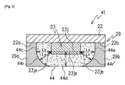
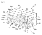
23 発光素子
23j p-nジャンクション
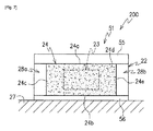
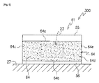
100,200,300 照明装置
1 蛍光体
24,64 第1光透過部材
29,29a,29b 第2光透過部材
25,55 第1カバー
26,56 第2カバー
Claims (11)
- p-nジャンクションを有する発光素子と、
蛍光体を含み、発光素子を封止し、互いに平行に位置する第1平行面および第2平行面と、第1平行面のエッジと第2平行面のエッジの間を、第1平行面と第2平行面に対して垂直に延びる、第1垂直面、第2垂直面、第3垂直面と、を備えた第1光透過部材と、
第1光透過部材の第1平行面上に配置されて、第1光透過部材の第1平行面と第1垂直面との間のエッジを越えて延び、さらに第1光透過部材の第1平行面と第2垂直面との間のエッジを越えて延びる第1カバーと、
第1光透過部材の第2平行面上に配置されて、第1光透過部材の第2平行面と第1垂直面との間のエッジを越えて延び、さらに第2平行面と第2垂直面との間のエッジを越えて延びる第2カバーと、
第1光透過部材の第1垂直面と第2垂直面にそれぞれ接触して配置され、かつ第1光透過部材よりも高い拡散係数を有する第2光透過部材と、を備え、
p-nジャンクションはp-nジャンクションの発光面において、第1光透過部材の第3垂直面に対向する、発光ダイオード。 - 第1光透過部材の第1平行面に配置された第1カバーは、厚みが第2カバーよりも厚い、請求項1に記載の発光ダイオード。
- 前記第2光透過部材は、第1光透過部材の第1垂直面及び第2垂直面と、第1カバー及び第2カバーとに接触している請求項1に記載の発光ダイオード。
- さらに、第1光透過部材の第3垂直面の反対側に位置し、かつ発光素子と電気的に接続された基板と、を備えた、請求項1に記載の発光ダイオード。
- p-nジャンクションと第1光透過部材の第1垂直面との間の距離は、p-nジャンクションと第1光透過部材の第3垂直面との間の距離と実質的に同一である、請求項1に記載の発光ダイオード。
- p-nジャンクションと第1光透過部材の第2垂直面との間の距離は、p-nジャンクションと第1光透過部材の第3垂直面との間の距離と実質的に同一である、請求項1に記載の発光ダイオード。
- p-nジャンクションと第1光透過部材の第1垂直面との間の距離は、p-nジャンクションと第1光透過部材の第3垂直面との間の距離よりも小さい、請求項1に記載の発光ダイオード。
- p-nジャンクションと第1光透過部材の第2垂直面との間の距離は、p-nジャンクションと第1光透過部材の第3垂直面との間の距離よりも小さい、請求項1に記載の発光ダイオード。
- 第1光透過部材は、第1垂直面と第3垂直面との間のサイドエッジにおいて丸みを帯びている、請求項1に記載の発光ダイオード。
- 第1光透過部材は、第2垂直面と第3垂直面との間のサイドエッジにおいて丸みを帯びている、請求項1に記載の発光ダイオード。
- マザーボードと、マザーボードに電気的に実装された基板を伴う請求項1に係る発光ダイオードと、を備え、発光ダイオードの第2カバーがマザーボードと接触している、照明装置。
Priority Applications (1)
| Application Number | Priority Date | Filing Date | Title |
|---|---|---|---|
| JP2014539175A JP6154392B2 (ja) | 2012-02-16 | 2013-02-18 | 発光ダイオードおよび発光ダイオードを有する照明装置 |
Applications Claiming Priority (6)
| Application Number | Priority Date | Filing Date | Title |
|---|---|---|---|
| JP2012031542 | 2012-02-16 | ||
| JP2012031542 | 2012-02-16 | ||
| JP2012031544 | 2012-02-16 | ||
| JP2012031544 | 2012-02-16 | ||
| JP2014539175A JP6154392B2 (ja) | 2012-02-16 | 2013-02-18 | 発光ダイオードおよび発光ダイオードを有する照明装置 |
| PCT/JP2013/000859 WO2013121800A1 (en) | 2012-02-16 | 2013-02-18 | Light-emitting diode and lighting device including the same |
Publications (3)
| Publication Number | Publication Date |
|---|---|
| JP2015510680A JP2015510680A (ja) | 2015-04-09 |
| JP2015510680A5 JP2015510680A5 (ja) | 2015-06-25 |
| JP6154392B2 true JP6154392B2 (ja) | 2017-06-28 |
Family
ID=48983928
Family Applications (1)
| Application Number | Title | Priority Date | Filing Date |
|---|---|---|---|
| JP2014539175A Expired - Fee Related JP6154392B2 (ja) | 2012-02-16 | 2013-02-18 | 発光ダイオードおよび発光ダイオードを有する照明装置 |
Country Status (5)
| Country | Link |
|---|---|
| US (1) | US9024518B2 (ja) |
| EP (1) | EP2815437B1 (ja) |
| JP (1) | JP6154392B2 (ja) |
| CN (1) | CN104137281B (ja) |
| WO (1) | WO2013121800A1 (ja) |
Families Citing this family (4)
| Publication number | Priority date | Publication date | Assignee | Title |
|---|---|---|---|---|
| KR102426861B1 (ko) * | 2015-12-02 | 2022-07-29 | 쑤저우 레킨 세미컨덕터 컴퍼니 리미티드 | 발광 소자 패키지 |
| JP7266961B2 (ja) | 2015-12-31 | 2023-05-01 | 晶元光電股▲ふん▼有限公司 | 発光装置 |
| JP6891530B2 (ja) * | 2017-02-20 | 2021-06-18 | 日亜化学工業株式会社 | 発光装置 |
| JP7284373B2 (ja) * | 2018-12-28 | 2023-05-31 | 日亜化学工業株式会社 | 発光装置 |
Family Cites Families (10)
| Publication number | Priority date | Publication date | Assignee | Title |
|---|---|---|---|---|
| JP2000208822A (ja) * | 1999-01-11 | 2000-07-28 | Matsushita Electronics Industry Corp | 半導体発光装置 |
| JP2004039778A (ja) | 2002-07-02 | 2004-02-05 | Matsushita Electric Ind Co Ltd | 照明用発光素子 |
| JP2004127604A (ja) | 2002-09-30 | 2004-04-22 | Citizen Electronics Co Ltd | 発光ダイオード及びバックライトユニット |
| KR100649679B1 (ko) * | 2005-07-19 | 2006-11-27 | 삼성전기주식회사 | 측면 발광형 엘이디 패키지 및 이를 이용한 백 라이트 유닛 |
| JP4956977B2 (ja) * | 2005-12-05 | 2012-06-20 | 日亜化学工業株式会社 | 発光装置 |
| JP2009032746A (ja) * | 2007-07-24 | 2009-02-12 | Harison Toshiba Lighting Corp | 発光装置及び発光ユニット |
| TWI401820B (zh) * | 2007-11-07 | 2013-07-11 | 財團法人工業技術研究院 | 發光元件及其製作方法 |
| JP5227613B2 (ja) * | 2008-02-27 | 2013-07-03 | スタンレー電気株式会社 | 半導体発光装置 |
| JP4808244B2 (ja) * | 2008-12-09 | 2011-11-02 | スタンレー電気株式会社 | 半導体発光装置およびその製造方法 |
| KR101615497B1 (ko) * | 2009-11-27 | 2016-04-27 | 삼성전자주식회사 | 발광소자 패키지 및 그 제조방법 |
-
2013
- 2013-02-18 EP EP13748752.6A patent/EP2815437B1/en active Active
- 2013-02-18 JP JP2014539175A patent/JP6154392B2/ja not_active Expired - Fee Related
- 2013-02-18 WO PCT/JP2013/000859 patent/WO2013121800A1/en not_active Ceased
- 2013-02-18 CN CN201380009387.0A patent/CN104137281B/zh not_active Expired - Fee Related
- 2013-02-18 US US13/885,595 patent/US9024518B2/en active Active
Also Published As
| Publication number | Publication date |
|---|---|
| WO2013121800A1 (en) | 2013-08-22 |
| EP2815437A4 (en) | 2015-11-04 |
| CN104137281B (zh) | 2017-09-08 |
| EP2815437A1 (en) | 2014-12-24 |
| EP2815437B1 (en) | 2019-08-14 |
| JP2015510680A (ja) | 2015-04-09 |
| US20140152172A1 (en) | 2014-06-05 |
| CN104137281A (zh) | 2014-11-05 |
| US9024518B2 (en) | 2015-05-05 |
Similar Documents
| Publication | Publication Date | Title |
|---|---|---|
| US9484509B2 (en) | Lighting device and method of manufacturing the same | |
| EP3413112B1 (en) | Optical lens and light emitting module having the same | |
| JP6164038B2 (ja) | 発光装置 | |
| JP6282438B2 (ja) | 半導体発光装置 | |
| CN108922884B (zh) | 发光二极管显示器 | |
| JP6361645B2 (ja) | 発光装置 | |
| TW201535797A (zh) | 發光裝置 | |
| JP2014072213A (ja) | 発光装置及びその製造方法 | |
| JP6154392B2 (ja) | 発光ダイオードおよび発光ダイオードを有する照明装置 | |
| WO2017047815A1 (ja) | 発光装置 | |
| CN107369674A (zh) | 发光二极管和发光模块 | |
| JP2013187357A (ja) | 反射光センサ | |
| JP5724183B2 (ja) | 発光装置 | |
| JP2015510680A5 (ja) | ||
| US9966413B2 (en) | Light-emitting diode module and lamp using the same | |
| JP6683000B2 (ja) | 発光装置及びその製造方法 | |
| JP2009266516A (ja) | レンズ付発光ユニット | |
| KR20130043899A (ko) | 발광소자 패키지 및 그 제조 방법 | |
| US20230317896A1 (en) | Light-emitting device | |
| US20180337215A1 (en) | Light-emitting assembly and method for producing a light-emitting assembly | |
| JP4861474B2 (ja) | 発光装置 | |
| KR102426861B1 (ko) | 발광 소자 패키지 | |
| KR101065455B1 (ko) | 엘이디 패키지 및 엘이디 패키지 제조방법 | |
| TWI389345B (zh) | Light emitting device | |
| TWI529969B (zh) | 發光二極體封裝結構 |
Legal Events
| Date | Code | Title | Description |
|---|---|---|---|
| A521 | Request for written amendment filed |
Free format text: JAPANESE INTERMEDIATE CODE: A523 Effective date: 20150422 |
|
| A621 | Written request for application examination |
Free format text: JAPANESE INTERMEDIATE CODE: A621 Effective date: 20150422 |
|
| A521 | Request for written amendment filed |
Free format text: JAPANESE INTERMEDIATE CODE: A523 Effective date: 20150507 |
|
| A131 | Notification of reasons for refusal |
Free format text: JAPANESE INTERMEDIATE CODE: A131 Effective date: 20160329 |
|
| A521 | Request for written amendment filed |
Free format text: JAPANESE INTERMEDIATE CODE: A523 Effective date: 20160524 |
|
| A131 | Notification of reasons for refusal |
Free format text: JAPANESE INTERMEDIATE CODE: A131 Effective date: 20161025 |
|
| A521 | Request for written amendment filed |
Free format text: JAPANESE INTERMEDIATE CODE: A523 Effective date: 20161221 |
|
| TRDD | Decision of grant or rejection written | ||
| A01 | Written decision to grant a patent or to grant a registration (utility model) |
Free format text: JAPANESE INTERMEDIATE CODE: A01 Effective date: 20170509 |
|
| A61 | First payment of annual fees (during grant procedure) |
Free format text: JAPANESE INTERMEDIATE CODE: A61 Effective date: 20170601 |
|
| R150 | Certificate of patent or registration of utility model |
Ref document number: 6154392 Country of ref document: JP Free format text: JAPANESE INTERMEDIATE CODE: R150 |
|
| R250 | Receipt of annual fees |
Free format text: JAPANESE INTERMEDIATE CODE: R250 |
|
| R250 | Receipt of annual fees |
Free format text: JAPANESE INTERMEDIATE CODE: R250 |
|
| LAPS | Cancellation because of no payment of annual fees |