JP6154392B2 - Light emitting diode and lighting device having light emitting diode - Google Patents
Light emitting diode and lighting device having light emitting diode Download PDFInfo
- Publication number
- JP6154392B2 JP6154392B2 JP2014539175A JP2014539175A JP6154392B2 JP 6154392 B2 JP6154392 B2 JP 6154392B2 JP 2014539175 A JP2014539175 A JP 2014539175A JP 2014539175 A JP2014539175 A JP 2014539175A JP 6154392 B2 JP6154392 B2 JP 6154392B2
- Authority
- JP
- Japan
- Prior art keywords
- light
- vertical surface
- cover
- light emitting
- transmission member
- Prior art date
- Legal status (The legal status is an assumption and is not a legal conclusion. Google has not performed a legal analysis and makes no representation as to the accuracy of the status listed.)
- Expired - Fee Related
Links
- 230000005540 biological transmission Effects 0.000 claims description 93
- 239000000758 substrate Substances 0.000 claims description 25
- OAICVXFJPJFONN-UHFFFAOYSA-N Phosphorus Chemical compound [P] OAICVXFJPJFONN-UHFFFAOYSA-N 0.000 claims description 15
- 238000009792 diffusion process Methods 0.000 claims description 7
- 239000011347 resin Substances 0.000 description 6
- 229920005989 resin Polymers 0.000 description 6
- 238000005286 illumination Methods 0.000 description 4
- 239000002245 particle Substances 0.000 description 3
- VYPSYNLAJGMNEJ-UHFFFAOYSA-N Silicium dioxide Chemical compound O=[Si]=O VYPSYNLAJGMNEJ-UHFFFAOYSA-N 0.000 description 2
- 230000002093 peripheral effect Effects 0.000 description 2
- 238000007789 sealing Methods 0.000 description 2
- 239000004593 Epoxy Substances 0.000 description 1
- 229910004298 SiO 2 Inorganic materials 0.000 description 1
- GWEVSGVZZGPLCZ-UHFFFAOYSA-N Titan oxide Chemical compound O=[Ti]=O GWEVSGVZZGPLCZ-UHFFFAOYSA-N 0.000 description 1
- PNEYBMLMFCGWSK-UHFFFAOYSA-N aluminium oxide Inorganic materials [O-2].[O-2].[O-2].[Al+3].[Al+3] PNEYBMLMFCGWSK-UHFFFAOYSA-N 0.000 description 1
- 239000003086 colorant Substances 0.000 description 1
- 239000011521 glass Substances 0.000 description 1
- 229910052751 metal Inorganic materials 0.000 description 1
- 239000002184 metal Substances 0.000 description 1
- 238000012986 modification Methods 0.000 description 1
- 230000004048 modification Effects 0.000 description 1
- 230000005855 radiation Effects 0.000 description 1
- 235000012239 silicon dioxide Nutrition 0.000 description 1
- 239000000377 silicon dioxide Substances 0.000 description 1
Images

Classifications
-
- H—ELECTRICITY
- H10—SEMICONDUCTOR DEVICES; ELECTRIC SOLID-STATE DEVICES NOT OTHERWISE PROVIDED FOR
- H10H—INORGANIC LIGHT-EMITTING SEMICONDUCTOR DEVICES HAVING POTENTIAL BARRIERS
- H10H20/00—Individual inorganic light-emitting semiconductor devices having potential barriers, e.g. light-emitting diodes [LED]
- H10H20/80—Constructional details
- H10H20/85—Packages
- H10H20/851—Wavelength conversion means
- H10H20/8515—Wavelength conversion means not being in contact with the bodies
-
- H—ELECTRICITY
- H10—SEMICONDUCTOR DEVICES; ELECTRIC SOLID-STATE DEVICES NOT OTHERWISE PROVIDED FOR
- H10H—INORGANIC LIGHT-EMITTING SEMICONDUCTOR DEVICES HAVING POTENTIAL BARRIERS
- H10H20/00—Individual inorganic light-emitting semiconductor devices having potential barriers, e.g. light-emitting diodes [LED]
- H10H20/80—Constructional details
- H10H20/85—Packages
- H10H20/851—Wavelength conversion means
- H10H20/8514—Wavelength conversion means characterised by their shape, e.g. plate or foil
-
- H—ELECTRICITY
- H10—SEMICONDUCTOR DEVICES; ELECTRIC SOLID-STATE DEVICES NOT OTHERWISE PROVIDED FOR
- H10H—INORGANIC LIGHT-EMITTING SEMICONDUCTOR DEVICES HAVING POTENTIAL BARRIERS
- H10H20/00—Individual inorganic light-emitting semiconductor devices having potential barriers, e.g. light-emitting diodes [LED]
- H10H20/80—Constructional details
- H10H20/85—Packages
- H10H20/855—Optical field-shaping means, e.g. lenses
-
- H—ELECTRICITY
- H10—SEMICONDUCTOR DEVICES; ELECTRIC SOLID-STATE DEVICES NOT OTHERWISE PROVIDED FOR
- H10H—INORGANIC LIGHT-EMITTING SEMICONDUCTOR DEVICES HAVING POTENTIAL BARRIERS
- H10H20/00—Individual inorganic light-emitting semiconductor devices having potential barriers, e.g. light-emitting diodes [LED]
- H10H20/80—Constructional details
- H10H20/84—Coatings, e.g. passivation layers or antireflective coatings
- H10H20/841—Reflective coatings, e.g. dielectric Bragg reflectors
-
- H—ELECTRICITY
- H10—SEMICONDUCTOR DEVICES; ELECTRIC SOLID-STATE DEVICES NOT OTHERWISE PROVIDED FOR
- H10H—INORGANIC LIGHT-EMITTING SEMICONDUCTOR DEVICES HAVING POTENTIAL BARRIERS
- H10H20/00—Individual inorganic light-emitting semiconductor devices having potential barriers, e.g. light-emitting diodes [LED]
- H10H20/80—Constructional details
- H10H20/85—Packages
- H10H20/852—Encapsulations
- H10H20/853—Encapsulations characterised by their shape
-
- H—ELECTRICITY
- H10—SEMICONDUCTOR DEVICES; ELECTRIC SOLID-STATE DEVICES NOT OTHERWISE PROVIDED FOR
- H10H—INORGANIC LIGHT-EMITTING SEMICONDUCTOR DEVICES HAVING POTENTIAL BARRIERS
- H10H20/00—Individual inorganic light-emitting semiconductor devices having potential barriers, e.g. light-emitting diodes [LED]
- H10H20/80—Constructional details
- H10H20/85—Packages
- H10H20/855—Optical field-shaping means, e.g. lenses
- H10H20/856—Reflecting means
Landscapes
- Led Device Packages (AREA)
Description
本発明は発光ダイオードに関連し、また、発光ダイオードを有する照明装置に関する。 The present invention relates to a light emitting diode and also relates to a lighting device having the light emitting diode.
素子基板と、素子基板上に実装された発光素子と、発光素子からの光を放ち、かつ発光素子を封止する封止体と、3次元軸であるX,Y,Zのうちいずれかの2軸の組み合わせから形成される2次元方向に封止体からの光を指向させる発光部を形成するための遮光手段と、を有する発光ダイオードが開示されている(日本特許公開公報 No. 2004-127604参照)。 An element substrate, a light emitting element mounted on the element substrate, a sealing body that emits light from the light emitting element and seals the light emitting element, and any one of X, Y, and Z that are three-dimensional axes A light-emitting diode having a light-shielding means for forming a light-emitting portion for directing light from a sealing body in a two-dimensional direction formed by a combination of two axes is disclosed (Japanese Patent Publication No. 2004- 127604).
また、発光デバイスチップと、発光デバイスチップを被覆する透明な部材と、発光デバイスチップからの光が出射される面を除いて、表面を被覆する反射部材と、を備えた発光装置が開示されている。その装置は、発光デバイスチップを通る少なくとも一の平面内において、発光デバイスチップから見た時に透明部材が180度以上の角度で露出されるように形成されている(日本特許公開公報 No. 2004-039778参照)。 Also disclosed is a light-emitting device comprising a light-emitting device chip, a transparent member that covers the light-emitting device chip, and a reflective member that covers the surface except for a surface from which light from the light-emitting device chip is emitted. Yes. The apparatus is formed such that the transparent member is exposed at an angle of 180 degrees or more when viewed from the light emitting device chip in at least one plane passing through the light emitting device chip (Japanese Patent Publication No. 2004- 039778 ).
発光ダイオードおよび/もしくは照明装置において、出射された光の方向によって、発光素子からと、光透過部材に含まれた蛍光体からとの、光のばらつきが生じる傾向がある。また、発光ダイオードおよび/もしくは広角で光を出射する構造を伴う照明装置において、必要としない方向へは光がもれないよう求められる。 In the light emitting diode and / or the lighting device, there is a tendency that light varies from the light emitting element and from the phosphor included in the light transmitting member depending on the direction of the emitted light. Further, in a lighting device having a light emitting diode and / or a structure that emits light at a wide angle, the light is required not to leak in an unnecessary direction.
本発明の第1の態様において、発光ダイオードは、p-nジャンクションを伴う発光素子と、蛍光体を含み、かつ発光素子を封止する第1の光透過部材と、第1の光透過部材の対向する面上に配置された第1カバーと第2カバーと、を備えている。第1カバーと第2カバーが第1の光透過部材の対向する面の縁を越えて延びていることが開示されている。 In the first aspect of the present invention, the light emitting diode includes: a light emitting element with a pn junction; a first light transmitting member that includes a phosphor and encapsulates the light emitting element; and A first cover and a second cover are provided on opposite surfaces. It is disclosed that the first cover and the second cover extend beyond the edges of the opposing surfaces of the first light transmission member.
本発明の第2の態様において、第1の光透過部材における第1の平行面上に配置された第1カバーは、第2カバーよりも厚みを厚くすることが可能である。 In the second aspect of the present invention, the first cover disposed on the first parallel surface of the first light transmitting member can be thicker than the second cover.
いくつかの実施形態において、第1光透過部材よりも高い拡散係数を有する第2光透過部材が、第1光透過部材の第1垂直面と接触して配置されていることが、開示されている。また、第1光透過部材よりも高い拡散係数を有する第2光透過部材が、第1光透過部材の第2垂直面と接触して配置されていることが、開示されている。 In some embodiments, it is disclosed that a second light transmissive member having a higher diffusion coefficient than the first light transmissive member is disposed in contact with a first vertical surface of the first light transmissive member. Yes. Further, it is disclosed that the second light transmission member having a higher diffusion coefficient than the first light transmission member is disposed in contact with the second vertical surface of the first light transmission member.
p-nジャンクションと第1光透過部材の第1垂直面との間の距離は、p-nジャンクションと第1光透過部材の第3垂直面との間の距離と実質的に同一であることが開示されている。p-nジャンクションと第1光透過部材の第2垂直面との間の距離は、p-nジャンクションと第1光透過部材の第3垂直面との間の距離と、実質的に同一であることが開示されている。 The distance between the pn junction and the first vertical surface of the first light transmission member is substantially the same as the distance between the pn junction and the third vertical surface of the first light transmission member. Is disclosed. The distance between the pn junction and the second vertical surface of the first light transmission member is substantially the same as the distance between the pn junction and the third vertical surface of the first light transmission member. It is disclosed.
さらに、p-nジャンクションと第1光透過部材の第1垂直面との間の距離は、p-nジャンクションと第1光透過部材の第3垂直面との間の距離よりも小さいことが開示されている。また、p-nジャンクションと第1光透過部材の第2垂直面との間の距離は、p-nジャンクションと第1光透過部材の第3垂直面との間の距離よりも小さいことが開示されている。 Furthermore, it is disclosed that the distance between the pn junction and the first vertical surface of the first light transmission member is smaller than the distance between the pn junction and the third vertical surface of the first light transmission member. Has been. Further, it is disclosed that the distance between the pn junction and the second vertical surface of the first light transmission member is smaller than the distance between the pn junction and the third vertical surface of the first light transmission member. Has been.
発光素子からおよび光透過部材に含まれた蛍光体からの、放射される方向による光のばらつきの発生を抑制することが可能となる。また、広角の出射角度で光を出すよう構成された発光ダイオードおよび/もしくは照明装置が提案される。 It is possible to suppress the occurrence of variation in light depending on the direction of emission from the light emitting element and from the phosphor included in the light transmitting member. In addition, a light emitting diode and / or a lighting device configured to emit light at a wide emission angle is proposed.
本明細書に使用されるように、「および/もしくは」という言葉は、関連して記載された項目の一つ、もしくは一つ以上の組み合わせのうちのいずれか、それらの組み合わせの全て、を含んでいる。
本明細書で使用される言葉は、それぞれの実施形態を描写する目的のために使用されるのであって、本発明の限定を意図するものではない。
As used herein, the term “and / or” includes any and all combinations of one or more of the associated listed items. It is out.
The terminology used herein is used for the purpose of describing each embodiment and is not intended to limit the present invention.
さらに、本明細書において、「発光素子」という言葉は、いくつかの実施形態において、ベアチップとしての、発光ダイオード(LED)素子として使用されても良い。ベアチップはウェハーレベルのチップであっても良い。 「発光素子」という言葉は、リードフレームに電気的に接続されるLED素子として使用されることも可能である。また、「発光素子」という言葉は、基板に電気的に接続されるLED素子として使用されることも可能である。 Further, in this specification, the term “light emitting element” may be used as a light emitting diode (LED) element as a bare chip in some embodiments. The bare chip may be a wafer level chip. The term “light emitting element” can also be used as an LED element that is electrically connected to a lead frame. The term “light emitting element” can also be used as an LED element electrically connected to a substrate.
発光素子は様々な色の光を出す発光素子の中から選択することが出来る。例えば、発光素子は青色発光素子でも良い。発光素子は紫外発光素子であっても良い。また、発光素子は赤色発光素子でも良い。さらには、発光素子は緑色や黄色発光の素子としても良い。 The light emitting element can be selected from light emitting elements that emit light of various colors. For example, the light emitting element may be a blue light emitting element. The light emitting element may be an ultraviolet light emitting element. The light emitting element may be a red light emitting element. Further, the light emitting element may be a green or yellow light emitting element.
本明細書で用いられる「〜の下の」や「〜の上の」、「上方の」や「下方の」のような相対語は、図に示される、ある要素、層、領域もしくは部分と、別の要素、層、領域もしくは部分との関係を描写するものとして使用されている場合がある。当然ながら、これらの言葉は、図に示される方向に加えて、装置の異なる向きを含むことを意図されている。 As used herein, relative terms such as “under”, “above”, “above”, and “below” refer to certain elements, layers, regions or portions shown in the figures. , May be used to depict a relationship with another element, layer, region or portion. Of course, these terms are intended to include different orientations of the device in addition to the orientation shown in the figures.
本発明の実施形態は、実施形態の示される添付の図面を参照して、以下に、より詳細に説明する。本発明は、しかしながら、多くの異なる形態において実施されることが可能であるので、ここに記載される実施形態に限定されるものとして解釈されるべきではない。そうではなく、これらの実施形態は、本開示を詳細で完全なものとし、本発明の範囲を当業者に詳細に伝えるために提示されるものである。 Embodiments of the present invention will be described in more detail below with reference to the accompanying drawings in which the embodiments are shown. The present invention, however, can be implemented in many different forms and should not be construed as limited to the embodiments set forth herein. Rather, these embodiments are provided so that this disclosure will be thorough and complete, and will fully convey the scope of the invention to those skilled in the art.
本発明の実施形態は、ここに含まれる図面を参照して説明される。同じおよび/もしくは類似の参照番号は、同じおよび/もしくは類似の構造を参照する。図面は、本来概略的なものであることに留意されるべきである。 Embodiments of the present invention will be described with reference to the drawings included herein. The same and / or similar reference numbers refer to the same and / or similar structures. It should be noted that the drawings are schematic in nature.
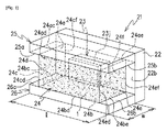
図1は本発明の第1実施形態に係る発光ダイオード(LED)21の上面斜視図を示す。LED21はp-nジャンクション23jを備えた発光素子23と、蛍光体1を含み、発光素子23を封止し、互いに平行な位置にある第1平行面24aと第2平行面24bとを有する第1光透過部材24と、を有している。LED21は、さらに、第1光透過部材24の第1平行面24aに配置された第1カバー25と、第1光透過部材24の第2平行面24b上に配置された第2カバー26とを有している。第1カバー25は、第1平行面24aに接触して配置され、第1平行面24aを上から覆っている。第2カバー26は、図1で示されるように、第2平行面24bに接触して配置され、第2平行面24bを下から覆っている。第1カバー25は、第1光透過部材24の第1平行面24aのエッジ24acおよび/もしくはエッジ24aeを越えて延びており、第2カバー26は、第1光透過部材24の第2平行面24bのエッジ24bcおよび/もしくはエッジ24beを越えて延びている。図1で示される第1カバー25は、第1光透過部材24の第1平行面24aに沿って真っすぐ延びている。図1で示される第2カバー26は、第1光透過部材24の第2平行面24bに沿って真っすぐ延びている。第1カバー25および第2カバー26は、図1内で両側を指す矢印「l」として示される反対方向に延びている。第1カバー25および第2カバー26は、両側を指す矢印「w」として示される反対方向においては、第1光透過部材24の面と平らに揃っていても良い。矢印「w」は矢印「l」に対して垂直に延びている。
FIG. 1 shows a top perspective view of a light emitting diode (LED) 21 according to a first embodiment of the present invention. The
詳細には、第1実施形態のLED21は、光を出すp-nジャンクション23jを有する発光素子23を備えている。LED21は、さらに、蛍光体1を含み、発光素子23を封止し、互いに平行に位置する第1平行面24aと第2平行面24bと、第1平行面24aのエッジ24ac、エッジ24aeおよびエッジ24adと第2平行面24bのエッジ24bc、24beおよび24bdとの間で第1平行面24aと第2平行面24bに対して垂直に延びる、第1垂直面24c、第2垂直面24eおよび第3垂直面24dとを有する第1光透過部材24と、を備えている。第1実施形態におけるLED21は、第1光透過部材24の第1平行面24aに配置された第1カバー25と、第1光透過部材24の第2平行面24bに配置された第2カバー26とをさらに備えている。第1カバー25は、第1光透過部材24の第1平行面24aと第1垂直面24cの間のエッジ24acを越えて延びており、第1光透過部材24の第1平行面24aと第2垂直面24eの間のエッジ24aeを越えて延びている。第2カバー26は、第1光透過部材24の第2平行面24bと第1垂直面24cの間のエッジ24bcを越えて延びており、第2平行面24bと第2垂直面24eの間のエッジ24beを越えて延びている。p-nジャンクション23jは、発光面23jsにおいて第1光透過部材24の第3垂直面24dと対向している。第1カバー25と第2カバー26は、光を閉じ込める樹脂から成るものとしても良い。例えば、その樹脂は不透明であっても良い。第1カバー25は、第1光透過部材24の第1平行面24aに接触する鏡面を有していても良い。さらに、第2カバー26は、第1光透過部材24の第2平行面24bと接触する鏡面を有していても良い。第1カバー25および/もしくは第2カバー26が有する鏡面によって、上方および/もしくは下方に向かう光を、第1光透過部材24の第1垂直面24c、第2垂直面24e、および第3垂直面24dを通過して出射される光の放射として利用することが可能となる。その結果、光の損失を抑えて、広角の光の放射を得ることが可能である。
Specifically, the
本実施形態において、光が、空気に取り囲まれた第3垂直面24d、第1垂直面24c、および第2垂直面24eを通過して広角な光を出射するように構成される。第1カバー25が、第1光透過部材24の第1平行面24aと第1垂直面24cの間のエッジ24acを越えて延びており、また、第1光透過部材24の第1平行面24aと第2垂直面24eの間のエッジ24aeを越えて延びているので、第1垂直面24cおよび/もしくは第2垂直面24eを通過して出射された上方および/もしくは下方へ向かう光は、第1カバー25および/もしくは第2カバー26で反射されて横方向の光とすることが出来る。その結果、光の損失を抑えて、横方向への広角の光の放射を得ることが出来る。また、不要な方向への光の漏出を防止することが出来る。
In the present embodiment, the light is configured to emit wide-angle light through the third
LED21は、さらに第1光透過部材24の第3垂直面24dの反対側に位置し、発光素子23と電気的に接続される基板22を備えていても良い。図1で示されるように、基板22は、第1光透過部材24の第4垂直面24fと接触して配置される。第4垂直面24fを覆う基板22は、第1カバー25と第2カバー26と互いに接触する部分で面が揃うようにして配置されている。その結果、基板22は、図1で両側を指す矢印「l」として示される両方向において、第1光透過部材24の第1垂直面24cと第4垂直面24fとの間のサイドエッジ24cfを越えて延びる第1延長部22aと、第1光透過部材24の第2垂直面24eと第4垂直面24fとの間のサイドエッジ24efを越えて延びる第2延長部22bとを有する。
The
LEDの実施形態において、発光素子23は基板22上に実装されていても良い。基板22はガラスエポキシ基板であっても良い。基板22は熱伝導性のある、アルミナから出来ていても良い。また、基板22は、発光素子23と熱的に接続することが出来る金属を含んでいても良い。基板22は、発光素子23のp-nジャンクション23jのp電極およびn電極と電気的に接続される電極を備えている。発光素子23のp電極およびn電極は、ワイヤーおよび/もしくはバンプによって、基板の電極に電気的に接続されていても良い。
In the LED embodiment, the
さらに、第1カバー25は、第1平行面24aと第1垂直面24cとの間のエッジ24acを越えて延びる第1延長部25aと、第1平行面24aと第2垂直面24eとの間のエッジ24aeを越えて延びる第2延長部25bとを有する。第2カバー26は、第2平行面24bと第1垂直面24cとの間のエッジ24bcを越えて延びる第1延長部26aと、第2平行面24bと第2垂直面24eとの間のエッジ24beを越えて延びる第2延長部26bと、を有する。その結果、発光素子23から出た光は180度に近い横方向の広角な光として放射されるよう構成される。
Further, the
p-nジャンクション23jの発光エッジ23jeにおけるp-nジャンクション23jと、第1光透過部材24の第1垂直面24cとの間の距離L2は、p-nジャンクション23jの発光面23jsにおけるp-nジャンクション23jと、第1光透過部材24の第3垂直面24dとの間の距離L1と実質的に等しくても良い。また、p-nジャンクション23jの発光エッジ23jeにおけるp-nジャンクション23jと、第1光透過部材24の第2垂直面24eとの間の距離L3は、p-nジャンクション23jの発光面23jsにおけるp-nジャンクション23jと、第1光透過部材24の第3垂直面24dとの間の距離L1と実質的に等しくても良い。
The distance L2 between the
さらに、p-nジャンクション23jの発光エッジ23jeにおけるp-nジャンクション23jと、第1光透過部材24の第1垂直面24cとの間の距離L2は、p-nジャンクション23jの発光面23jsと第1光透過部材24の第3垂直面24dとの間の距離L1よりも小さくすることも可能である。また、p-nジャンクション23jの発光エッジ23jeにおけるp-nジャンクション23jと、第1光透過部材24の第2垂直面24eとの間の距離L3は、p-nジャンクション23jの発光面23jsにおけるp-nジャンクション23jと、第1光透過部材24の第3垂直面24dとの間の距離L1よりも小さくすることも可能である。p-nジャンクション23jは、発光面23jsにおいて、第1光透過部材24の第3垂直面24dに対向し、p-nジャンクション23jは、発光エッジ23jeにおいて、第1垂直面24cと第2垂直面24eに対向するので、p-nジャンクション23jから第3垂直面24dに向けて出射された光の強さは、p-nジャンクション23jから第1垂直面24cもしくは第2垂直面24eに向けて出射された光の強さよりも強くなることが考えられる。したがって、第1垂直面24cおよび/もしくは第2垂直面24eに向かう方向では、第1光透過部材24の第3垂直面24dに向かう方向に比べて、蛍光体1を含む第1光透過部材24の厚みを薄くすることが可能である。
Further, the distance L2 between the
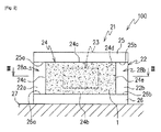
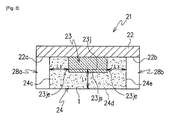
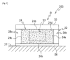
図2は、図1で示され、照明装置100のマザーボード27に実装されたLED21の正面図を示す。また、図3は、図2のIII−III線で切り取ったLED21の断面図を示す。照明装置100は、横方向に広角な光を出す光源を必要とする表示装置であっても良い。また、照明装置100は、横方向に広角な光を出す光源を必要とする照明システムであっても良い。図2で示されるように、第1光透過部材24の第3垂直面24dは、第1カバー25と第2カバー26との周辺側面と面一となっていても良いが、第1光透過部材24の第1垂直面24cおよび第2垂直面24eは、第1カバー25および第2カバー26の周辺側面よりも内側に位置している。したがって、第1カバー25の第1延長部25aと、第1光透過部材24の第1垂直面24c、基板22の第1延長部22aと、第2カバー26の第1延長部26aによって画定される第1スペース28aがあり、第1カバー25の第2延長部25bと、第1光透過部材24の第2垂直面24eと、基板22の第2延長部22bと、第2カバー26の第2延長部26bによって画定される第2スペース28bがある。第2カバー26がマザーボード27に実装される際に、基板22はマザーボードに接触もしくは隣り合う部分があっても良い。その結果、マザーボード27を介して、基板22および発光素子23へ電流供給が可能である。
FIG. 2 is a front view of the
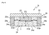
図4は本発明の第2実施形態に係るLED31の断面図を示す。LED31は、p-nジャンクション23jを有する発光素子23と、蛍光体1を含み発光素子23を封止し、互いに平行に位置する第1平行面24aと第2平行面24bとを有する第1光透過部材24と、を備えている。第1光透過部材24は透明もしくは半透明の樹脂から成り、発光素子23から出た光によって励起され得る蛍光体1を含む。LED21は、さらに第1光透過部材24の第1平行面24a上に配置された第1カバー25と、第1光透過部材24の第2平行面24b上に配置された第2カバー26とを有する。第1カバー25は第1光透過部材24の第1平行面24aのエッジ24acおよび/もしくはエッジ24aeを越えて延びており、第2カバー26は、第1光透過部材24の第2平行面24bのエッジ24bcおよび/もしくはエッジ24beを越えて延びている。
FIG. 4 shows a cross-sectional view of the
第1カバー25と第2カバー26は光を通さない樹脂から成るものとすることが出来る。例えば、この樹脂は不透明なものとしても良い。第1カバー25が、第1光透過部材24の第1平行面24aと接触する鏡面を有していても良い。鏡面は、第1光透過部材24からの光を反射させて第1光透過部材24に戻すことが可能である。鏡面は、第1カバー25の第1延長部25aおよび第2延長部25bを覆うように延長されることも可能である。さらに、第2カバー26は第1光透過部材24の第2平行面24bと接触する鏡面を有していても良い。鏡面は、第2カバー26の第1延長部26aと第2延長部26bを覆うように延長されることも可能である。第1カバー25および/もしくは第2カバー26が鏡面を有する場合、上方および/もしくは下方に向かう光を、横方向の光として第1垂直面24c、第2垂直面24e、および第3垂直面24dから、出射することが可能である。結果として、光の損失を抑えた横方向の広角な光の出射が可能となり得る。
The
本実施形態においては、第1実施形態とは異なり、LED31は、さらに、第1カバー25と第2カバー26との間の第1光透過部材24に接触して配置された、第1光透過部材よりも拡散係数の高い第2光透過部材29と、を備えている。第2光透過部材29は反射粒子を含むことが可能である。反射粒子は二酸化ケイ素(SiO2)から出来ていても良い。反射粒子は二酸化チタン(TiO2)から出来ていても良い。第2光透過部材29は、第1光透過部材24の第1垂直面24cと、第1カバー25と、第2カバー26と接触して配置される。すなわち、第2光透過部材29は、第1カバー25と、第1垂直面24cと、基板22と、第2カバー26とによって画定される第1スペース28a内に充填される。また、第1光透過部材24よりも高い拡散係数を有する第2光透過部材29は、第1光透過部材24の第2垂直面24eと、第1カバー25と、第2カバー26とに接触して配置される。すなわち、第2光透過部材29は、第1カバー25と、第2垂直面24eと、基板22と、第2カバー26によって画定される第2スペース28b内に充填される。
In the present embodiment, unlike the first embodiment, the
第1光透過部材24の第1垂直面24cと接触して配置された第2光透過部材29と、第1光透過部材24の第2垂直面24eと接触して配置された第2光透過部材29は、第1光透過部材24により、離れて配置される。第2光透過部材29が配置されて、発光素子23からの光と蛍光体1からの光が拡散され得るので、発光素子23と蛍光体1からの光のばらつきの発生を抑えることが可能である。また、第2光透過部材29は、第1カバー25により上方から、第2カバー26により下方からはさまれるので、光の損失を抑えた広角の横方向の光の放射を得ることが可能になる。
The second
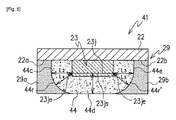
図5は、本発明の第3実施形態に係るLED41の断面図を示す。本実施形態において、第1光透過部材44は、第1垂直面44cと第3垂直面44dの間のサイドエッジが丸みを帯びている。また、第1光透過部材44は、第2垂直面44eと第3垂直面44dとの間のサイドエッジが丸みを帯びている。この実施形態において、第1光透過部材44の丸みを帯びた部分の光は、サイドエッジにおいて、発光素子23からの光と蛍光体1からの光のばらつきの発生を抑える可能性がある。
FIG. 5 shows a cross-sectional view of an LED 41 according to the third embodiment of the present invention. In the present embodiment, the first
本実施形態において、p-nジャンクション23jの発光エッジ23jeと第1光透過部材44の丸みを帯びた部分44rとの間の距離L4は、距離L1と実質的に同じであっても良い。p-nジャンクション23jの発光エッジ23jeと第1光透過部材44の丸みを帯びた部分44r’は、距離L1と実質的に同じであっても良い。
In the present embodiment, the distance L4 between the light emitting edge 23je of the
本実施形態において、第1光透過部材44よりも高い光拡散係数を有する第2光透過部材29(29aとして図示)は、第1光透過部材44の第1垂直面44cと接触して配置されていても良い。第2光透過部材29は、丸みを帯びた部分44rのところまで覆っていても良い。また、第1光透過部材44よりも高い光拡散係数を有する第2光透過部材29(29bとして図示)は、さらに第1光透過部材44の第2垂直面44eと接触して配置されている。第2光透過部材29は、丸みを帯びた部分44r’のところまで覆っていても良い。 したがって、第1カバー25の第1延長部25aと、第1垂直面24c、および第2カバー26の第1延長部26aとによって画定される第1スペース28aは第2光透過部材29(29aとして図示)によって満たされており、また、第1カバー25の第2延長部25bと、第2垂直面24eと、第2カバー26の第2延長部26bによって画定される第2スペース28bは、第2光透過部材29(29bとして図示)によって満たされている。
In the present embodiment, the second light transmission member 29 (shown as 29 a) having a light diffusion coefficient higher than that of the first
図6は、本発明の第4実施形態に係るLED51の上面斜視図を示す。図7は、図6に図示され、照明装置200のマザーボード27に実装されたLED51の正面図を示す。発光ダイオード(LED)51は、p-nジャンクション23jを伴う発光素子23と、蛍光体1を含み発光素子23を封止し、互いに平行に位置する第1平行面24aと第2平行面24bとを有する第1光透過部材24と、を備えている。LED51は、第1光透過部材24の第1平行面24aに配置された第1カバー55と、第1光透過部材24の第2平行面24bに配置された第2カバー56と、を有している。第1カバー55は、第1光透過部材24の第1平行面24aのエッジ24acおよび/もしくはエッジ24aeを越えて延びており、また、第2カバー56は、第1光透過部材24の第2平行面のエッジ24bcおよび/もしくはエッジ24beを越えて延びている。
FIG. 6 is a top perspective view of an
本実施形態において、第1光透過樹脂24の第1平行面24aに配置された第1カバー55は、第2カバー56よりも厚みがある。
In the present embodiment, the
第2カバー56が照明装置200のマザーボード27上に配置される場合、マザーボード27の方向に向かう光はマザーボード上で反射および/もしくは吸収され得るが、第1カバー55の方向に向かう光については、部分的に第1カバー55を通過して出てしまうことがあるかもしれない。そこで、第1カバー55において光もれを防止するために、第1カバー55は第2カバー56よりも厚みを大きく設けている。
When the
図8は、本発明の第5実施形態に係るLED61の上面斜視図を示し、図9は、図8に示され、照明装置300のマザーボード27上に実装されたLED61の正面図を示す。
FIG. 8 shows a top perspective view of the
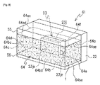
LED61は、p-nジャンクション23jを有する発光素子23と、蛍光体1を含み発光素子23を封止し、互いに平行に位置する第1平行面64aと第2平行面64bと、第1垂直面64cと、第2垂直面64eと、第3垂直面64dと、を有する第1光透過部材64と、を備えている。第1垂直面64cと、第2垂直面64eと、第3垂直面64dは、第1平行面64aのエッジ64ac,64ae,64adと第2平行面64bのエッジ64bc,64be,64deの間を、第1平行面64aと第2平行面64bに対して垂直に延びている。
The
LED61は、さらに、第1光透過部材64の第1平行面64aに配置される第1カバー55と、第1光透過部材64の第2平行面64bに配置される第2カバー56とを有している。発光素子23のp-nジャンクション23jは、その発光面23jsにおいて、第1光透過部材64の第3垂直面64dに対向する。第1光透過部材64の第1平行面64aに設けられた第1カバー55は第2カバー56よりも厚みが大きい。
The
本実施形態では、空気によって取り囲まれている、第3垂直面64dと、第1垂直面64cと、第2垂直面64eを通過して、光は側面方向に広角で出射されるように構成されている。LED61は、さらに、第1光透過部材64の第3垂直面64dの反対側に位置し、発光素子23と電気的に接続される基板22を備えていても良い。この構造により、空気によって取り囲まれている第3垂直面64dと、第1垂直面64cと、第2垂直面64eを透過して、光は側面方向に広角で出射されるように構成されている。LED61は、さらに、第1光透過部材64の第3垂直面64dの反対側に位置し、発光素子23と電気的に接続される基板22を備えていても良い。図8に示されるように、基板22は第1光透過部材64の第4垂直面64fに接触して位置している。第4垂直面64fを覆う基板22は第1光透過部材64と、第1カバー55と、第2カバー56と互いに接触して隣設された部分で面一となって配置されている。
In the present embodiment, light passes through the third
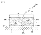
図9に示されるように、第2カバー56が照明装置100のマザーボード27上に配置される場合、マザーボード27に向かう光はマザーボード27上で反射されおよび/もしくは吸収され得るが、第1カバー55に向かう光の一部が第1カバー55を通過して漏光するかもしれない。そのため、第1カバー55は、マザーボード27に隣設して位置するよう構成された第2カバー56よりも厚みを大きくしている。
As shown in FIG. 9, when the
さらに、本発明の主題からいくつかの実施形態が要素の特定の組み合わせを参照して図示されているが、本発明の主題の教示から離れることなく様々な組み合わせが他にも可能である。したがって、本発明の主題はここに記載されて図面に図示された例示的実施形態に限定されるものとして解釈されるべきではなく、様々な図示された実施形態の要素の組み合わせを包含するものでもある。 Further, although some embodiments from the subject matter of the present invention have been illustrated with reference to particular combinations of elements, various other combinations are possible without departing from the teachings of the subject matter of the present invention. Accordingly, the subject matter of the present invention should not be construed as limited to the exemplary embodiments described herein and illustrated in the drawings, but may include combinations of elements of the various illustrated embodiments. is there.
本発明の開示を前提として、本発明の主題となる趣旨と範囲から逸脱することなく、当業者によって多くの変更および改変がなされることが可能である。それゆえ、図示された実施形態は例示の目的のためだけに示されたものであって、また添付された特許請求の範囲によって定義される発明の主題を限定するものとして考えられるべきではない、ということが理解されねばならない。添付された特許請求の範囲は、したがって、文字通り記載されている要素の組み合わせだけでなく、実質的に同じ結果を得るために実質的に同じ方法で実質的に同じ機能を奏する、全ての等価要素を含むものとして解釈されるべきである。特許請求の範囲は、それゆえに、具体的に図示して上に説明されたものも、概念的に均等なものも、また、発明の主題の本質的な概念を組み入れるものも、含むと解釈されるべきである。 Given the disclosure of the present invention, many changes and modifications can be made by those skilled in the art without departing from the spirit and scope of the subject matter of the invention. Therefore, the illustrated embodiments are shown for illustrative purposes only and should not be considered as limiting the subject matter of the invention as defined by the appended claims. It must be understood. The appended claims therefore cover not only literally described combinations of elements, but also all equivalent elements that perform substantially the same function in substantially the same way to obtain substantially the same result. Should be interpreted as including. The claims are therefore to be construed to include what is specifically illustrated and described above, what is conceptually equivalent, and what incorporates the essential concepts of the inventive subject matter. Should be.
本発明の実施形態に係るLEDを有する照明装置は、広角に光を放射する光源を必要とする表示装置であっても良い。また、本発明の実施形態に係るLEDを有する照明装置は、広角に光を放射する光源を必要とする照明システムであっても良い。 The illumination device having the LED according to the embodiment of the present invention may be a display device that requires a light source that emits light at a wide angle. Moreover, the illuminating device which has LED which concerns on embodiment of this invention may be an illuminating system which requires the light source which radiates | emits light at a wide angle.
21,31,41,51,61 発光ダイオード(LED)
23 発光素子
23j p-nジャンクション
100,200,300 照明装置
1 蛍光体
24,64 第1光透過部材
29,29a,29b 第2光透過部材
25,55 第1カバー
26,56 第2カバー
21, 31, 41, 51, 61 Light emitting diode (LED)
23 light emitting
Claims (11)
蛍光体を含み、発光素子を封止し、互いに平行に位置する第1平行面および第2平行面と、第1平行面のエッジと第2平行面のエッジの間を、第1平行面と第2平行面に対して垂直に延びる、第1垂直面、第2垂直面、第3垂直面と、を備えた第1光透過部材と、
第1光透過部材の第1平行面上に配置されて、第1光透過部材の第1平行面と第1垂直面との間のエッジを越えて延び、さらに第1光透過部材の第1平行面と第2垂直面との間のエッジを越えて延びる第1カバーと、
第1光透過部材の第2平行面上に配置されて、第1光透過部材の第2平行面と第1垂直面との間のエッジを越えて延び、さらに第2平行面と第2垂直面との間のエッジを越えて延びる第2カバーと、
第1光透過部材の第1垂直面と第2垂直面にそれぞれ接触して配置され、かつ第1光透過部材よりも高い拡散係数を有する第2光透過部材と、を備え、
p-nジャンクションはp-nジャンクションの発光面において、第1光透過部材の第3垂直面に対向する、発光ダイオード。 a light emitting device having a pn junction;
A first parallel surface and a second parallel surface which contain a phosphor and seal the light emitting element and are positioned in parallel to each other; a first parallel surface between an edge of the first parallel surface and an edge of the second parallel surface; A first light transmissive member comprising a first vertical surface, a second vertical surface, and a third vertical surface extending perpendicularly to the second parallel surface;
The first light transmitting member is disposed on the first parallel surface, extends beyond the edge between the first parallel surface and the first vertical surface of the first light transmitting member, and further includes a first light transmitting member first. A first cover extending beyond the edge between the parallel plane and the second vertical plane;
It is disposed on the second parallel surface of the first light transmission member, extends beyond the edge between the second parallel surface and the first vertical surface of the first light transmission member, and further, the second parallel surface and the second vertical surface. A second cover extending beyond the edge between the surface;
A second light transmission member disposed in contact with each of the first vertical surface and the second vertical surface of the first light transmission member and having a diffusion coefficient higher than that of the first light transmission member,
The pn junction is a light emitting diode that faces the third vertical surface of the first light transmitting member on the light emitting surface of the pn junction.
A lighting device comprising: a motherboard; and a light emitting diode according to claim 1 with a substrate electrically mounted on the motherboard, wherein the second cover of the light emitting diode is in contact with the motherboard.
Priority Applications (1)
| Application Number | Priority Date | Filing Date | Title |
|---|---|---|---|
| JP2014539175A JP6154392B2 (en) | 2012-02-16 | 2013-02-18 | Light emitting diode and lighting device having light emitting diode |
Applications Claiming Priority (6)
| Application Number | Priority Date | Filing Date | Title |
|---|---|---|---|
| JP2012031542 | 2012-02-16 | ||
| JP2012031542 | 2012-02-16 | ||
| JP2012031544 | 2012-02-16 | ||
| JP2012031544 | 2012-02-16 | ||
| JP2014539175A JP6154392B2 (en) | 2012-02-16 | 2013-02-18 | Light emitting diode and lighting device having light emitting diode |
| PCT/JP2013/000859 WO2013121800A1 (en) | 2012-02-16 | 2013-02-18 | Light-emitting diode and lighting device including the same |
Publications (3)
| Publication Number | Publication Date |
|---|---|
| JP2015510680A JP2015510680A (en) | 2015-04-09 |
| JP2015510680A5 JP2015510680A5 (en) | 2015-06-25 |
| JP6154392B2 true JP6154392B2 (en) | 2017-06-28 |
Family
ID=48983928
Family Applications (1)
| Application Number | Title | Priority Date | Filing Date |
|---|---|---|---|
| JP2014539175A Expired - Fee Related JP6154392B2 (en) | 2012-02-16 | 2013-02-18 | Light emitting diode and lighting device having light emitting diode |
Country Status (5)
| Country | Link |
|---|---|
| US (1) | US9024518B2 (en) |
| EP (1) | EP2815437B1 (en) |
| JP (1) | JP6154392B2 (en) |
| CN (1) | CN104137281B (en) |
| WO (1) | WO2013121800A1 (en) |
Families Citing this family (4)
| Publication number | Priority date | Publication date | Assignee | Title |
|---|---|---|---|---|
| KR102426861B1 (en) * | 2015-12-02 | 2022-07-29 | 쑤저우 레킨 세미컨덕터 컴퍼니 리미티드 | Light emitting device package |
| JP7266961B2 (en) * | 2015-12-31 | 2023-05-01 | 晶元光電股▲ふん▼有限公司 | light emitting device |
| JP6891530B2 (en) * | 2017-02-20 | 2021-06-18 | 日亜化学工業株式会社 | Light emitting device |
| JP7284373B2 (en) * | 2018-12-28 | 2023-05-31 | 日亜化学工業株式会社 | light emitting device |
Family Cites Families (10)
| Publication number | Priority date | Publication date | Assignee | Title |
|---|---|---|---|---|
| JP2000208822A (en) * | 1999-01-11 | 2000-07-28 | Matsushita Electronics Industry Corp | Semiconductor light emitting device |
| JP2004039778A (en) | 2002-07-02 | 2004-02-05 | Matsushita Electric Ind Co Ltd | Lighting element for lighting |
| JP2004127604A (en) * | 2002-09-30 | 2004-04-22 | Citizen Electronics Co Ltd | Light emitting diode and backlight unit |
| KR100649679B1 (en) * | 2005-07-19 | 2006-11-27 | 삼성전기주식회사 | Side-emitting LED package and backlight unit using same |
| JP4956977B2 (en) * | 2005-12-05 | 2012-06-20 | 日亜化学工業株式会社 | Light emitting device |
| JP2009032746A (en) | 2007-07-24 | 2009-02-12 | Harison Toshiba Lighting Corp | Light emitting device and light emitting unit |
| TWI401820B (en) * | 2007-11-07 | 2013-07-11 | 財團法人工業技術研究院 | Light-emitting element and manufacturing method thereof |
| JP5227613B2 (en) * | 2008-02-27 | 2013-07-03 | スタンレー電気株式会社 | Semiconductor light emitting device |
| JP4808244B2 (en) * | 2008-12-09 | 2011-11-02 | スタンレー電気株式会社 | Semiconductor light emitting device and manufacturing method thereof |
| KR101615497B1 (en) * | 2009-11-27 | 2016-04-27 | 삼성전자주식회사 | Light Emitting Diode Package and Method of Manufacturing The Same |
-
2013
- 2013-02-18 JP JP2014539175A patent/JP6154392B2/en not_active Expired - Fee Related
- 2013-02-18 EP EP13748752.6A patent/EP2815437B1/en active Active
- 2013-02-18 WO PCT/JP2013/000859 patent/WO2013121800A1/en not_active Ceased
- 2013-02-18 CN CN201380009387.0A patent/CN104137281B/en not_active Expired - Fee Related
- 2013-02-18 US US13/885,595 patent/US9024518B2/en active Active
Also Published As
| Publication number | Publication date |
|---|---|
| CN104137281B (en) | 2017-09-08 |
| US9024518B2 (en) | 2015-05-05 |
| EP2815437A4 (en) | 2015-11-04 |
| JP2015510680A (en) | 2015-04-09 |
| EP2815437A1 (en) | 2014-12-24 |
| US20140152172A1 (en) | 2014-06-05 |
| EP2815437B1 (en) | 2019-08-14 |
| CN104137281A (en) | 2014-11-05 |
| WO2013121800A1 (en) | 2013-08-22 |
Similar Documents
| Publication | Publication Date | Title |
|---|---|---|
| US9484509B2 (en) | Lighting device and method of manufacturing the same | |
| EP3413112B1 (en) | Optical lens and light emitting module having the same | |
| JP6164038B2 (en) | Light emitting device | |
| JP5915483B2 (en) | Light emitting device and manufacturing method thereof | |
| JP6282438B2 (en) | Semiconductor light emitting device | |
| CN108922884B (en) | LED display | |
| TW201535797A (en) | Illuminating device | |
| JP6154392B2 (en) | Light emitting diode and lighting device having light emitting diode | |
| WO2017047815A1 (en) | Light-emitting device | |
| CN107369674A (en) | Light emitting diode and light emitting module | |
| JP2013187357A (en) | Reflection light sensor | |
| JP2025065479A (en) | Light receiving element, light emitting device | |
| JP5081708B2 (en) | Light-emitting unit with lens | |
| JP2015510680A5 (en) | ||
| JP6683000B2 (en) | Light emitting device and manufacturing method thereof | |
| US9966413B2 (en) | Light-emitting diode module and lamp using the same | |
| KR20130043899A (en) | Light emitting device package and manufacturing method using the same | |
| US20230317896A1 (en) | Light-emitting device | |
| US10541267B2 (en) | Light-emitting assembly and method for producing a light-emitting assembly | |
| JP4861474B2 (en) | Light emitting device | |
| KR101065455B1 (en) | LED package and manufacturing method of LED package | |
| TWI389345B (en) | Light emitting device | |
| TWI529969B (en) | Light emitting diode package structure | |
| CN120712923A (en) | Light-emitting device and display device | |
| KR20170064898A (en) | Light emitting device package |
Legal Events
| Date | Code | Title | Description |
|---|---|---|---|
| A521 | Request for written amendment filed |
Free format text: JAPANESE INTERMEDIATE CODE: A523 Effective date: 20150422 |
|
| A621 | Written request for application examination |
Free format text: JAPANESE INTERMEDIATE CODE: A621 Effective date: 20150422 |
|
| A521 | Request for written amendment filed |
Free format text: JAPANESE INTERMEDIATE CODE: A523 Effective date: 20150507 |
|
| A131 | Notification of reasons for refusal |
Free format text: JAPANESE INTERMEDIATE CODE: A131 Effective date: 20160329 |
|
| A521 | Request for written amendment filed |
Free format text: JAPANESE INTERMEDIATE CODE: A523 Effective date: 20160524 |
|
| A131 | Notification of reasons for refusal |
Free format text: JAPANESE INTERMEDIATE CODE: A131 Effective date: 20161025 |
|
| A521 | Request for written amendment filed |
Free format text: JAPANESE INTERMEDIATE CODE: A523 Effective date: 20161221 |
|
| TRDD | Decision of grant or rejection written | ||
| A01 | Written decision to grant a patent or to grant a registration (utility model) |
Free format text: JAPANESE INTERMEDIATE CODE: A01 Effective date: 20170509 |
|
| A61 | First payment of annual fees (during grant procedure) |
Free format text: JAPANESE INTERMEDIATE CODE: A61 Effective date: 20170601 |
|
| R150 | Certificate of patent or registration of utility model |
Ref document number: 6154392 Country of ref document: JP Free format text: JAPANESE INTERMEDIATE CODE: R150 |
|
| R250 | Receipt of annual fees |
Free format text: JAPANESE INTERMEDIATE CODE: R250 |
|
| R250 | Receipt of annual fees |
Free format text: JAPANESE INTERMEDIATE CODE: R250 |
|
| LAPS | Cancellation because of no payment of annual fees |