JP2013187357A - Reflection light sensor - Google Patents

Reflection light sensor Download PDF

Info

Publication number
JP2013187357A
JP2013187357A JP2012051389A JP2012051389A JP2013187357A JP 2013187357 A JP2013187357 A JP 2013187357A JP 2012051389 A JP2012051389 A JP 2012051389A JP 2012051389 A JP2012051389 A JP 2012051389A JP 2013187357 A JP2013187357 A JP 2013187357A
Authority
JP
Japan
Prior art keywords
light
emitting element
receiving element
light emitting
light receiving
Prior art date
Legal status (The legal status is an assumption and is not a legal conclusion. Google has not performed a legal analysis and makes no representation as to the accuracy of the status listed.)
Pending
Application number
JP2012051389A
Other languages
Japanese (ja)
Inventor
Fumio Ogawa
文雄 小川
Current Assignee (The listed assignees may be inaccurate. Google has not performed a legal analysis and makes no representation or warranty as to the accuracy of the list.)
Stanley Electric Co Ltd
Original Assignee
Stanley Electric Co Ltd
Priority date (The priority date is an assumption and is not a legal conclusion. Google has not performed a legal analysis and makes no representation as to the accuracy of the date listed.)
Filing date
Publication date
Application filed by Stanley Electric Co Ltd filed Critical Stanley Electric Co Ltd
Priority to JP2012051389A priority Critical patent/JP2013187357A/en
Publication of JP2013187357A publication Critical patent/JP2013187357A/en
Pending legal-status Critical Current

Links

Images

Abstract

PROBLEM TO BE SOLVED: To solve the problem that, even when a groove defined by two side surfaces vertical to a luminous surface is formed between a light-emitting element and a light-receiving element, the amount of light directly incident on the light-receiving element through a resin layer among the light emitted from the light-emitting element is still large, and that, therefore, the S/N ratio of a reflection light sensor is small.SOLUTION: A light-emitting element 1 and a light-receiving element 2 are mounted on a wiring board 3, which are further encapsulated by a light permeable (visible rays cut) resin layer 4. An ∠-shaped groove 5 is formed whose side surface S1 on the light-emitting element 1 side is perpendicular to a luminous surface and whose side surface S2' of the light-receiving element 2 side is inclined to the light-receiving element 2 side relative to the luminous surface. The incident angle relative to the side surface S2' of light L1 from the light-emitting element 1 passing through the vertical side surface S1 and arriving at the side surface S2' via the air (groove 5) increases. As a result, the amount of light L1 reflected at the side surface S2' becomes large, which results in the amount of light entering the light-receiving element 2 directly from the light-emitting element 1 being reduced. Thus, the S/N ratio of a reflection light sensor can be improved.

Description

本発明は表面実装型の反射光センサに関する。   The present invention relates to a surface mount type reflected light sensor.

一般に、反射光センサは、発光素子及び受光素子を備え、発光素子からの発光を被検出物に照射し、その反射光を受光素子で受光し、これにより、被検出物の存否を検出する。   In general, a reflected light sensor includes a light emitting element and a light receiving element, irradiates a detected object with light emitted from the light emitting element, and receives the reflected light by the light receiving element, thereby detecting the presence or absence of the detected object.

図14は従来の反射光センサを示し、(A)は上面図、(B)は(A)のB−B線断面図である。図14においては、発光素子101及び受光素子102を光透過性樹脂層103によって封止し、かつ発光素子101と受光素子102との間の樹脂層103に発光面に対して両側面S1,S2が垂直な溝部104を設けていた(参照:特許文献1の第4図、特許文献2の第1図)。これにより、発光素子101からの発光が樹脂層103を通って受光素子102に直接入射しないようにし、反射光センサの信号/雑音(S/N)比を向上させていた。尚、103a、103bは樹脂層103によって形成される発光素子101、受光素子102に対するレンズである。   14A and 14B show a conventional reflected light sensor, where FIG. 14A is a top view and FIG. 14B is a cross-sectional view taken along the line BB of FIG. In FIG. 14, the light-emitting element 101 and the light-receiving element 102 are sealed with a light-transmitting resin layer 103, and both side surfaces S1 and S2 are formed on the resin layer 103 between the light-emitting element 101 and the light-receiving element 102 with respect to the light-emitting surface. Is provided with a vertical groove 104 (see: FIG. 4 of Patent Document 1 and FIG. 1 of Patent Document 2). This prevents light emitted from the light emitting element 101 from directly entering the light receiving element 102 through the resin layer 103, thereby improving the signal / noise (S / N) ratio of the reflected light sensor. Reference numerals 103 a and 103 b denote lenses for the light emitting element 101 and the light receiving element 102 formed by the resin layer 103.

特開昭59−56779号公報JP 59-56779 A 特開昭62−132377号公報Japanese Patent Laid-Open No. 62-132377

しかしながら、上述の従来の反射光センサにおいては、発光素子101からの発光のうち樹脂層103及び溝部104を通って受光素子102へ直接入射する光量は依然として多く、従って、光センサのS/N比は依然として小さいという課題があった。   However, in the above-described conventional reflected light sensor, the amount of light directly incident on the light receiving element 102 through the resin layer 103 and the groove 104 out of the light emitted from the light emitting element 101 is still large, and accordingly, the S / N ratio of the light sensor. There was still the problem of being small.

すなわち、一般的に、屈折率が変化する側面S1、S2では、光はスネルの屈折反射法則に従って屈折及び反射するが、その際、入射角θ11、θ12;θ21、θ22が大きくなるにつれて光の反射量が増加する一方、光の屈折量が減少する。また、側面S1では入射角が臨界角以上のときのみ光は全反射する。   That is, in general, on the side surfaces S1 and S2 where the refractive index changes, light is refracted and reflected according to Snell's law of refraction and reflection. At this time, the reflection of light increases as the incident angles θ11 and θ12; θ21 and θ22 increase. While the amount increases, the amount of light refraction decreases. On the side surface S1, light is totally reflected only when the incident angle is equal to or greater than the critical angle.

従って、図14の(A)、(B)において、発光素子101から樹脂層103を通って側面S1に斜めに到達した光L1、L2は側面S1にて反射しその反射量は側面S1に対する入射角θ1に応じた量であり、また、これらの光L1、L2のうち側面S1にて屈折して空気(溝部104)を透過して側面S2に斜めに到達した光L1、L2は側面S2にて反射しその反射量は側面S2に対する入射角θ12、θ22に応じた量である。従って、光L1、L2のうち側面S2にて屈折して樹脂層103に再び入り込む光の光量は小さくなる。しかしながら、図14の(A)における発光素子101から樹脂層103を通って側面S1に直角に到達した光L3は側面S1に対する入射角がほぼ0°であるので、光L3のほぼ全光量が側面S1において屈折して空気(溝部104)を透過し、側面S2に到達する。このときも、光L3の側面S2に対する入射角もほぼ0°であるので、光L3のほぼ全光量が側面S2にて屈折して再び樹脂層103に入り込む。光L3の入り込みはS/N比の点で問題となる。このようにして、たとえ発光面に対して側面S1、S2よりなる溝部104を発光素子101と受光素子102との間に設けても、再び樹脂層103に入り込んだ光が樹脂層103の内壁で反射して発光素子101から受光素子102へ直接入射する光の光量の減少は依然として小さく、従って、反射光センサのS/N比は依然として小さい。   Accordingly, in FIGS. 14A and 14B, light L1 and L2 that have obliquely reached the side surface S1 from the light emitting element 101 through the resin layer 103 are reflected by the side surface S1, and the amount of reflection is incident on the side surface S1. The amount of light L1 and L2 is refracted at the side surface S1 and transmitted through the air (groove 104) and reaches the side surface S2 obliquely on the side surface S2. The amount of reflection is an amount corresponding to the incident angles θ12 and θ22 with respect to the side surface S2. Therefore, the light quantity of the light L1 and L2 that is refracted at the side surface S2 and enters the resin layer 103 again becomes small. However, the light L3 that reaches the side surface S1 at right angles from the light emitting element 101 in FIG. 14A through the resin layer 103 has an incident angle of about 0 ° with respect to the side surface S1, so that almost all the light amount of the light L3 is on the side surface. In S1, the light is refracted and passes through the air (groove 104) to reach the side surface S2. Also at this time, since the incident angle of the light L3 with respect to the side surface S2 is substantially 0 °, almost the entire light amount of the light L3 is refracted by the side surface S2 and enters the resin layer 103 again. The entry of the light L3 becomes a problem in terms of the S / N ratio. In this way, even if the groove portion 104 formed of the side surfaces S1 and S2 is provided between the light emitting element 101 and the light receiving element 102 with respect to the light emitting surface, the light that has entered the resin layer 103 again on the inner wall of the resin layer 103. The decrease in the amount of light reflected and directly incident on the light receiving element 102 from the light emitting element 101 is still small, and thus the S / N ratio of the reflected light sensor is still small.

上述の課題を解決するために、本発明に係る反射光センサは、基板上に形成された発光素子及び受光素子と、発光素子及び受光素子を封止する光透過性樹脂層とを具備する反射光センサにおいて、光透過性樹脂層は、発光素子と受光素子との間に形成された溝部を有し、溝部を構成する発光素子に対向する第1の面及び受光素子に対向する第2の面の少なくとも1つの面は、溝部の断面において、発光素子との距離が溝部の上方に向って大きくなるように受光素子側に傾斜していることを特徴とするものである。これにより、発光素子から傾斜した面に到達した光のこの傾斜した面に対する入射角が大きくなる。   In order to solve the above-described problems, a reflected light sensor according to the present invention includes a light emitting element and a light receiving element formed on a substrate, and a reflective resin layer that seals the light emitting element and the light receiving element. In the optical sensor, the light-transmitting resin layer has a groove formed between the light emitting element and the light receiving element, and has a first surface facing the light emitting element constituting the groove and a second surface facing the light receiving element. At least one of the surfaces is characterized in that in the cross section of the groove portion, the surface is inclined toward the light receiving element side so that the distance from the light emitting element increases toward the upper side of the groove portion. Thereby, the incident angle with respect to this inclined surface of the light which reached the inclined surface from the light emitting element becomes large.

また、上述の第1の面及び第2の面の少なくとも1つの面には、溝部の上方から見て、発光素子の中心と受光素子の中心とを結ぶ線に垂直な面に対して傾斜した傾斜領域が形成されている。この傾斜領域は、溝部の上方から見て、受光素子から発光素子に向って突出するように湾曲して形成されている。あるいは、傾斜領域は、溝部の上方から見て、受光素子から発光素子に向って突出する2つの面として形成されている。あるいは、傾斜領域は、溝部の上方から見て、発光素子の中心と受光素子の中心とを結ぶ線に斜めに交差する面として形成されている。   Further, at least one of the first surface and the second surface described above is inclined with respect to a surface perpendicular to a line connecting the center of the light emitting element and the center of the light receiving element when viewed from above the groove. An inclined region is formed. The inclined region is formed to be curved so as to protrude from the light receiving element toward the light emitting element when viewed from above the groove. Alternatively, the inclined region is formed as two surfaces protruding from the light receiving element toward the light emitting element when viewed from above the groove. Alternatively, the inclined region is formed as a plane that obliquely intersects with a line connecting the center of the light emitting element and the center of the light receiving element when viewed from above the groove.

さらに、上述の発光素子及び受光素子は発光素子の一側面と受光素子の一側面とが対向するように基板上に搭載され、上述の第1の面及び第2の面の少なくとも1つの面には、溝部を上方から見て、発光素子の受光素子に対向した側面に対して傾斜した傾斜領域が形成されている。この傾斜領域は、溝部の上方から見て、受光素子から発光素子に向って突出する傾斜した湾曲面として形成されている。あるいは、傾斜領域は、溝部の上方から見て、受光素子から発光素子に向って突出する傾斜した2つの傾斜面として形成されている。あるいは、傾斜領域は、溝部の上方から見て、発光素子の中心と受光素子の中心とを結ぶ線に斜めに交差する傾斜面として形成されている。   Further, the light emitting element and the light receiving element described above are mounted on the substrate so that one side surface of the light emitting element and one side surface of the light receiving element face each other, and the light emitting element and the light receiving element are provided on at least one of the first surface and the second surface. Is formed with an inclined region that is inclined with respect to the side surface of the light emitting element facing the light receiving element when viewed from above. The inclined region is formed as an inclined curved surface that protrudes from the light receiving element toward the light emitting element when viewed from above the groove. Alternatively, the inclined region is formed as two inclined surfaces that protrude from the light receiving element toward the light emitting element when viewed from above the groove. Alternatively, the inclined region is formed as an inclined surface that obliquely intersects with a line connecting the center of the light emitting element and the center of the light receiving element when viewed from above the groove.

さらに、上述の傾斜領域は、溝部の上方から見て、発光素子の中心と受光素子の中心とを結ぶ線に交差する部分領域に形成されている。この場合、溝部は、基板上から見て、発光素子の中心と受光素子の中心とを結ぶ線に交差する部分領域でこの線に対して傾斜し、この部分領域の外側の領域でこの線に対して垂直となっている。   Further, the above-described inclined region is formed in a partial region intersecting with a line connecting the center of the light emitting element and the center of the light receiving element when viewed from above the groove. In this case, the groove portion is inclined with respect to this line in a partial region intersecting with a line connecting the center of the light emitting element and the center of the light receiving element when viewed from above the substrate, and the groove portion extends to this line in a region outside the partial region. It is perpendicular to it.

本発明によれば、発光素子からの光の溝部を構成する第1、第2の面の少なくとも1つの面に対する入射角が大きくなるので、第1、第2の面の少なくとも1つの面における反射光の光量は多くなり、この結果、発光素子から受光素子へ直接入射する光の光量は減少し、従って、反射光のS/N比を向上できる。   According to the present invention, since the incident angle with respect to at least one of the first and second surfaces constituting the groove portion of the light from the light emitting element is increased, reflection on at least one of the first and second surfaces is performed. The amount of light increases, and as a result, the amount of light directly incident on the light receiving element from the light emitting element decreases, and therefore the S / N ratio of reflected light can be improved.

本発明に係る反射光センサの第1の実施の形態を示し、(A)は斜視図、(B)は上面図、(C)は(B)のC-C線断面図である。1A and 1B show a first embodiment of a reflected light sensor according to the present invention, in which FIG. 3A is a perspective view, FIG. 3B is a top view, and FIG. 本発明に係る反射光センサの第2の実施の形態を示し、(A)は斜視図、(B)は上面図、(C)は(B)のC-C線断面図である。The 2nd Embodiment of the reflected light sensor which concerns on this invention is shown, (A) is a perspective view, (B) is a top view, (C) is CC sectional view taken on the line of (B). 本発明に係る反射光センサの第3の実施の形態を示し、(A)は斜視図、(B)は上面図、(C)は(B)のC-C線断面図である。3A and 3B show a third embodiment of a reflected light sensor according to the present invention, in which FIG. 3A is a perspective view, FIG. 3B is a top view, and FIG. 本発明に係る反射光センサの第4の実施の形態を示し、(A)は斜視図、(B)は上面図、(C)は(B)のC-C線断面図である。4A and 4B show a reflected light sensor according to a fourth embodiment of the present invention, in which FIG. 5A is a perspective view, FIG. 5B is a top view, and FIG. 本発明に係る反射光センサの第5の実施の形態を示し、(A)は斜視図、(B)は上面図、(C)は(B)のC-C線断面図である。5 shows a fifth embodiment of a reflected light sensor according to the present invention, (A) is a perspective view, (B) is a top view, and (C) is a sectional view taken along the line CC of (B). FIG. 本発明に係る反射光センサの第6の実施の形態を示し、(A)は斜視図、(B)は上面図、(C)は(B)のC-C線断面図である。6 shows a sixth embodiment of the reflected light sensor according to the present invention, wherein (A) is a perspective view, (B) is a top view, and (C) is a cross-sectional view taken along the line CC of (B). FIG. 本発明に係る反射光センサの第7の実施の形態を示し、(A)は斜視図、(B)は上面図、(C)は(B)のC-C線断面図である。7 shows a reflected light sensor according to a seventh embodiment of the present invention, in which (A) is a perspective view, (B) is a top view, and (C) is a sectional view taken along the line CC of (B). FIG. 本発明に係る反射光センサの第8の実施の形態を示し、(A)は斜視図、(B)は上面図、(C)は(B)のC-C線断面図である。FIG. 8 shows an eighth embodiment of the reflected light sensor according to the present invention, in which (A) is a perspective view, (B) is a top view, and (C) is a sectional view taken along the line CC of (B). 本発明に係る反射光センサの第9の実施の形態を示し、(A)は斜視図、(B)は上面図、(C)は(B)のC-C線断面図である。The 9th Embodiment of the reflected light sensor which concerns on this invention is shown, (A) is a perspective view, (B) is a top view, (C) is CC sectional view taken on the line of (B). 本発明に係る反射光センサの第10の実施の形態を示し、(A)は斜視図、(B)は上面図、(C)は(B)のC-C線断面図である。The 10th Embodiment of the reflected light sensor which concerns on this invention is shown, (A) is a perspective view, (B) is a top view, (C) is CC sectional view taken on the line of (B). 本発明に係る反射光センサの第11の実施の形態を示し、(A)は斜視図、(B)は上面図、(C)は(B)のC-C線断面図である。11 shows an eleventh embodiment of a reflected light sensor according to the present invention, in which (A) is a perspective view, (B) is a top view, and (C) is a sectional view taken along the line CC of (B). FIG. 本発明に係る反射光センサの第12の実施の形態を示し、(A)は斜視図、(B)は上面図、(C)は(B)のC-C線断面図である。The 12th Embodiment of the reflected light sensor which concerns on this invention is shown, (A) is a perspective view, (B) is a top view, (C) is CC sectional view taken on the line of (B). 図1の(B)の変更例を示す上面図である。It is a top view which shows the example of a change of (B) of FIG. 従来の反射光センサを示し、(A)は上面図、(B)は(A)のB-B線断面図である。The conventional reflected light sensor is shown, (A) is a top view, (B) is the BB sectional drawing of (A).

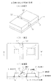
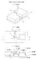
図1は本発明に係る反射光センサの第1の実施の形態を示し、(A)は斜視図、(B)は上面図、(C)は(B)のC-C線断面図である。   1A and 1B show a first embodiment of a reflected light sensor according to the present invention, in which FIG. 1A is a perspective view, FIG. 1B is a top view, and FIG. 1C is a sectional view taken along the line CC of FIG. .

図1においては、発光素子1、受光素子2を配線基板3上に実装し、さらに、光透過性(発光素子1の発光波長が赤外領域の場合には、可視光カットが好ましい)の樹脂層4にて封止している。さらに、図14の溝部104の代わりに、発光素子1側の側面S1が発光素子1の上面に対して垂直(発光素子1の受光素子2側の側面に平行)であり受光素子2側の側面S2’が発光素子1の受光素子2側の側面に対して受光素子2側に該側面との距離が溝部5の上方に向かって大きくなるように傾斜した傾斜面である断面レ字型溝部5を設けてある。溝部5は、樹脂層4の発光素子1と受光素子2との間に、樹脂層4の上面から配線基板3に向けて形成されている。このレ字型溝部5は樹脂層4をトランスファ成型する際に金型で形成してもよく、または、トランスファ成型後にレーザ加工で形成してもよい。このレーザ加工の場合、レーザ加工面が黒化(炭化)すると遮光性が高くなるので、炭酸ガスレーザ等のハイパワーレーザ加工が適している。溝部5は、底部が発光素子1の上面より低い位置まで達していることが好ましく、受光素子2の上面より低い位置まで達していることが好ましい。また、溝部5は、配線基板3まで達してもよい。   In FIG. 1, a light-emitting element 1 and a light-receiving element 2 are mounted on a wiring board 3, and further, a light-transmitting resin (a visible light cut is preferable when the light-emitting wavelength of the light-emitting element 1 is in the infrared region). Sealed with layer 4. Further, instead of the groove portion 104 in FIG. 14, the side surface S1 on the light emitting element 1 side is perpendicular to the upper surface of the light emitting element 1 (parallel to the side surface on the light receiving element 2 side of the light emitting element 1). S2 ′ is a cross-sectionally-shaped groove portion 5 which is an inclined surface inclined so that the distance from the side surface to the light receiving element 2 side of the light emitting element 1 on the light receiving element 2 side increases toward the upper side of the groove portion 5. Is provided. The groove portion 5 is formed between the light emitting element 1 and the light receiving element 2 of the resin layer 4 from the upper surface of the resin layer 4 toward the wiring substrate 3. The letter-shaped groove 5 may be formed by a mold when the resin layer 4 is transfer molded, or may be formed by laser processing after transfer molding. In the case of this laser processing, when the laser processed surface is blackened (carbonized), the light shielding property is increased, and therefore high power laser processing such as a carbon dioxide laser is suitable. The bottom of the groove 5 preferably reaches a position lower than the upper surface of the light emitting element 1, and preferably reaches a position lower than the upper surface of the light receiving element 2. Further, the groove 5 may reach the wiring board 3.

尚、図1において、発光素子1は赤外線発光ダイオード(LED)素子、受光素子2はフォトダイオード素子、フォトトランジスタ素子等、配線基板3はガラスエポキシ基板等をベースとし、発光素子1および受光素子2への給電用の配線パターン(図示せず)が形成されている。樹脂層4はエポキシ樹脂、シリコーン樹脂等よりなる。6はカーボンブラック等の遮光材料入りの遮光性ダイアタッチ材料層、7は受光素子2の側面から上端面を覆う金属層である。遮光性ダイアタッチ材料層6は受光素子2側の樹脂層4に入り込んだ迷光及び溝部5より深い樹脂層4に入り込んだ光が受光素子2に入射しないようにする。また、金属層7は受光素子2の上面以外からの入射光を遮光するためのものであり、S/N比の向上に役立つ。尚、金属層7を形成する受光素子2の肩部分をメサエッチングすることにより金属層7のクラックを防止する。また、図示しない金、銀、または銅等のワイヤよりなるボンディングワイヤにより発光素子1、受光素子2の電極と配線基板3の配線パターンとを接続する。   In FIG. 1, the light emitting element 1 is an infrared light emitting diode (LED) element, the light receiving element 2 is a photodiode element, a phototransistor element, etc., and the wiring board 3 is based on a glass epoxy substrate or the like. A wiring pattern (not shown) for supplying power to the battery is formed. The resin layer 4 is made of an epoxy resin, a silicone resin, or the like. Reference numeral 6 denotes a light-shielding die attach material layer containing a light-shielding material such as carbon black, and 7 denotes a metal layer that covers the upper surface from the side surface of the light receiving element 2. The light-shielding die attach material layer 6 prevents stray light entering the resin layer 4 on the light receiving element 2 side and light entering the resin layer 4 deeper than the groove 5 from entering the light receiving element 2. The metal layer 7 is for shielding incident light from other than the upper surface of the light receiving element 2, and is useful for improving the S / N ratio. Note that the metal layer 7 is prevented from cracking by mesa-etching the shoulder portion of the light receiving element 2 forming the metal layer 7. Further, the electrodes of the light emitting element 1 and the light receiving element 2 and the wiring pattern of the wiring board 3 are connected by a bonding wire made of a wire such as gold, silver, or copper (not shown).

図1の(C)に示すごとく、発光素子1から側面S1を通って空気(溝部5)を介して側面S2’に到達した光L1の側面S2’に対する入射角は図14の(B)における光L1の側面S2に対する入射角より大きくなる。ここで、光L1は、発光素子1から溝部5の発光素子1側の側面S1を通り、溝部5の受光素子2側の側面S2’に到達する光のうち、配線基板3の上面と平行な光より発光素子1から上方に放出される光を示す。この結果、光L1の側面S2’における反射光の光量は図14の(B)における光L1の側面S2における反射光量より多くなり、この結果、発光素子1から受光素子2へ直接入射する光の光量は減少し、従って、反射光センサのS/N比を向上できる。   As shown in FIG. 1C, the incident angle with respect to the side surface S2 ′ of the light L1 that has reached the side surface S2 ′ from the light emitting element 1 through the side surface S1 through the air (groove 5) is as shown in FIG. It becomes larger than the incident angle with respect to the side surface S2 of the light L1. Here, the light L1 passes through the side surface S1 on the light emitting element 1 side of the groove portion 5 from the light emitting element 1 and reaches the side surface S2 ′ on the light receiving element 2 side of the groove portion 5 and is parallel to the upper surface of the wiring board 3. The light emitted upward from the light emitting element 1 than the light is shown. As a result, the amount of reflected light on the side surface S2 ′ of the light L1 is larger than the amount of reflected light on the side surface S2 of the light L1 in FIG. 14B. As a result, the light directly incident on the light receiving element 2 from the light emitting element 1 The amount of light decreases, and therefore the S / N ratio of the reflected light sensor can be improved.

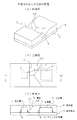
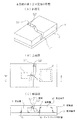
図2は本発明に係る反射光センサの第2の実施の形態を示し、(A)は斜視図、(B)は上面図、(C)は(B)のC-C線断面図である。   2A and 2B show a second embodiment of a reflected light sensor according to the present invention, in which FIG. 2A is a perspective view, FIG. 2B is a top view, and FIG. 2C is a sectional view taken along the line CC of FIG. .

図2においては、図14の溝部104の代わりに、発光素子1側の側面S1’が発光素子1の受光素子2側の側面に対して受光素子2側に該側面(発光素子の受光素子側の側面)との距離が溝部5’の上方に向かって大きくなるように傾斜した傾斜面であり、受光素子2側の側面S2が発光素子1の上面に対して垂直(発光素子1の受光素子2側の側面に平行)である断面ム字型溝部5’を設けてある。溝部5’は、樹脂層4の発光素子1と受光素子2との間に、樹脂層4の上面から配線基板3に向けて形成されている。このム字型溝部5’は樹脂層4をトランスファ成型後にレーザ加工で形成する。このレーザ加工の場合、レーザ加工面が黒化(炭化)すると遮光性が高くなるので、炭酸ガスレーザ等のハイパワーレーザ加工が適している。   In FIG. 2, instead of the groove 104 in FIG. 14, the side surface S1 ′ on the light emitting element 1 side is closer to the light receiving element 2 side than the side surface on the light receiving element 2 side of the light emitting element 1 (the light receiving element side of the light emitting element). The side surface S2 on the light receiving element 2 side is perpendicular to the upper surface of the light emitting element 1 (the light receiving element of the light emitting element 1). A cross-sectional groove-shaped groove portion 5 ′ that is parallel to the side surface on the second side is provided. The groove 5 ′ is formed between the light emitting element 1 and the light receiving element 2 of the resin layer 4 from the upper surface of the resin layer 4 toward the wiring substrate 3. The m-shaped groove 5 'is formed by laser processing after the resin layer 4 is transfer molded. In the case of this laser processing, when the laser processed surface is blackened (carbonized), the light shielding property is increased, and therefore high power laser processing such as a carbon dioxide laser is suitable.

図2の(C)に示すごとく、発光素子1から側面S1’に到達した光L1の側面S1’に対する入射角は図14の(B)における光L1の側面S1に対する入射角より大きくなる。この結果、光L1の側面S1’における反射光の光量は図14の(B)の光L1の側面S1における反射光の光量より多くなり、この結果、発光素子1から受光素子2へ直接入射する光の光量は減少し、従って、反射光センサのS/N比を向上できる。   As shown in FIG. 2C, the incident angle of the light L1 reaching the side surface S1 'from the light emitting element 1 with respect to the side surface S1' is larger than the incident angle of the light L1 with respect to the side surface S1 in FIG. As a result, the amount of reflected light on the side surface S1 ′ of the light L1 becomes larger than the amount of reflected light on the side surface S1 of the light L1 in FIG. 14B, and as a result, the light L1 directly enters the light receiving element 2. The amount of light is reduced, and therefore the S / N ratio of the reflected light sensor can be improved.

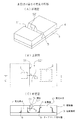
図3は本発明に係る反射光センサの第3の実施の形態を示し、(A)は斜視図、(B)は上面図、(C)は(B)のC-C線断面図である。   3A and 3B show a third embodiment of the reflected light sensor according to the present invention, in which FIG. 3A is a perspective view, FIG. 3B is a top view, and FIG. 3C is a sectional view taken along the line CC of FIG. .

図3においては、図14の溝部104の代わりに、発光素子1側の側面S1’及び受光素子2側の側面S2’が共に発光素子1の受光素子2側の側面に対して受光素子2側に該側面(発光素子1の受光素子2側の側面)との距離が溝部5’’の上方に向かって大きくなるように傾斜した側面である溝部5’’を設けてある。溝部5”は、樹脂層4の発光素子1と受光素子2との間に、樹脂層4の上面から配線基板3に向けて形成されている。この溝部5’’は樹脂層4をトランスファ成型する際に金型で形成してもよく、または、トランスファ成型後にレーザ加工で形成してもよい。このレーザ加工の場合、レーザ加工面が黒化(炭化)すると遮光性が高くなるので、炭酸ガスレーザ等のハイパワーレーザ加工が適している。   In FIG. 3, instead of the groove 104 in FIG. 14, the side surface S1 ′ on the light emitting element 1 side and the side surface S2 ′ on the light receiving element 2 side are both on the light receiving element 2 side with respect to the side surface on the light receiving element 2 side. A groove portion 5 ″ that is an inclined side surface is provided so that the distance from the side surface (the side surface of the light emitting element 1 on the light receiving element 2 side) increases toward the upper side of the groove portion 5 ″. The groove portion 5 ″ is formed between the light emitting element 1 and the light receiving element 2 of the resin layer 4 from the upper surface of the resin layer 4 toward the wiring substrate 3. The groove portion 5 ″ is formed by transfer molding the resin layer 4. In the case of laser processing, if the laser processing surface is blackened (carbonized), the light shielding property is increased. High power laser processing such as gas laser is suitable.

図3の(C)に示すごとく、発光素子1から側面S1’に到達した光L1の側面S1’に対する入射角は図14の(B)における光L1の側面S1に対する入射角より大きくなると共に、側面S1’を通って空気(溝部5”)を介して側面S2’に到達した光L1の側面S2’に対する入射角も図14の(B)における光L1の側面S2に対する入射角より大きくなる。この結果、光L1の側面S1’、S2’における反射光の光量は図14の(B)の光L1の側面S1、S2における反射光の光量より多くなり、この結果、発光素子1から受光素子2へ直接入射する光の光量は減少し、従って、反射光センサのS/N比を向上できる。   As shown in FIG. 3C, the incident angle of the light L1 reaching the side surface S1 ′ from the light emitting element 1 with respect to the side surface S1 ′ is larger than the incident angle of the light L1 with respect to the side surface S1 in FIG. The incident angle of the light L1 that has reached the side surface S2 ′ through the side surface S1 ′ through the air (groove 5 ″) with respect to the side surface S2 ′ is also larger than the incident angle of the light L1 with respect to the side surface S2 in FIG. As a result, the amount of reflected light on the side surfaces S1 ′ and S2 ′ of the light L1 is greater than the amount of reflected light on the side surfaces S1 and S2 of the light L1 in FIG. The amount of light directly incident on 2 is reduced, so that the S / N ratio of the reflected light sensor can be improved.

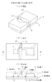
図4は本発明に係る反射光センサの第4の実施の形態を示し、(A)は斜視図、(B)は上面図、(C)は(B)のC-C線断面図である。尚、第4の実施の形態の側面S2’は第1の実施の形態の反射光センサの側面S2’を受光素子2を囲むようなR形状を有するように形成したものである。側面S2’は、配線基板3の上方から観測して、受光素子2側から発光素子1側に向かって突出するような湾曲面として形成されている。本実施の形態において、側面S2’は、発光素子1の受光素子2側の側面および溝部5の発光素子1側の側面S1に対して傾斜した面で形成されている。第4の実施の形態における溝部5の側面S2’の形状は図2、図3の反射光センサの側面S2、側面S2’にも適用できる。   4A and 4B show a fourth embodiment of a reflected light sensor according to the present invention, in which FIG. 4A is a perspective view, FIG. 4B is a top view, and FIG. 4C is a cross-sectional view taken along the line CC of FIG. . The side surface S <b> 2 ′ of the fourth embodiment is formed so that the side surface S <b> 2 ′ of the reflected light sensor of the first embodiment has an R shape surrounding the light receiving element 2. The side surface S <b> 2 ′ is formed as a curved surface that projects from the light receiving element 2 side toward the light emitting element 1 side when observed from above the wiring board 3. In the present embodiment, the side surface S2 'is formed as a surface that is inclined with respect to the side surface of the light emitting element 1 on the light receiving element 2 side and the side surface S1 of the groove 5 on the light emitting element 1 side. The shape of the side surface S2 'of the groove 5 in the fourth embodiment can also be applied to the side surface S2 and the side surface S2' of the reflected light sensor of FIGS.

図4の(B)に示すごとく、発光素子1から側面S1を通って空気(溝部5)を介して側面S2’に到達した光L2の側面S2’に対する入射角は図14の(A)における光L2の側面S2に対する入射角より大きくなる。ここで、光L2は、発光素子1からの溝部5の発光素子1側の側面を通り、溝部5の受光素子2側の側面に到達する光のうち、樹脂層4の上方から見て(上面図、図4の(B)において)、側面S2’における発光素子1の中心と受光素子2の中心を結ぶ線に垂直な面に対して傾斜した領域に入射した光を示す。この結果、光L2の側面S2’における反射光の光量は図14の(A)における光L2の側面S2における反射光量より多くなり、この結果、発光素子1から受光素子2へ直接入射する光の光量は減少し、従って、反射光センサのS/N比を向上できる。   As shown in FIG. 4B, the incident angle with respect to the side surface S2 ′ of the light L2 that has reached the side surface S2 ′ from the light emitting element 1 through the side surface S1 through the air (groove portion 5) is as shown in FIG. It becomes larger than the incident angle with respect to the side surface S2 of the light L2. Here, the light L2 passes through the side surface of the groove portion 5 from the light emitting element 1 on the light emitting element 1 side and reaches the side surface of the groove portion 5 on the light receiving element 2 side as viewed from above the resin layer 4 (upper surface). FIG. 4B shows light incident on a side surface S2 ′ that is incident on a region inclined with respect to a plane perpendicular to a line connecting the center of the light emitting element 1 and the center of the light receiving element 2. As a result, the amount of reflected light on the side surface S2 ′ of the light L2 is greater than the amount of reflected light on the side surface S2 of the light L2 in FIG. 14A. As a result, the light directly incident on the light receiving element 2 from the light emitting element 1 The amount of light decreases, and therefore the S / N ratio of the reflected light sensor can be improved.

図1に示す第1の実施の形態と同様、溝部5を構成する受光素子2側の側面S2’が、発光素子1の受光素子2側の側面に対して受光素子2側に該側面との距離が溝部5の上方に向かい大きくなるよう傾斜している。そのため、発光素子1の受光素子2側の側面に平行な場合と比較して、発光素子1から放出された光のうち、側面S1を通過して側面S2’へ入射する光の入射角が大きくなるので、側面S2’における反射光量が大きくなり、受光素子2への入射光量が減少し、反射光センサのS/N比を向上することができる。   As in the first embodiment shown in FIG. 1, the side surface S <b> 2 ′ on the light receiving element 2 side that forms the groove 5 is located on the light receiving element 2 side with respect to the side surface on the light receiving element 2 side. The distance is inclined so as to increase toward the upper side of the groove portion 5. Therefore, compared with the case where the light emitting element 1 is parallel to the side surface on the light receiving element 2 side, the incident angle of the light emitted from the light emitting element 1 and incident on the side surface S2 ′ through the side surface S1 is larger. Therefore, the amount of reflected light at the side surface S2 ′ increases, the amount of incident light on the light receiving element 2 decreases, and the S / N ratio of the reflected light sensor can be improved.

さらに、受光素子2側の側面S2’は、溝部5を上方から観測した場合において(図4の(B)参照)、発光素子1の中心と受光素子2の中心を結ぶ線に垂直な面に対して傾斜した領域を有する。つまり、受光素子2側の側面S2’は、発光素子1側の側面S1に対し傾斜した領域が形成されている。そのため、従来(図14(A))や第1の実施の形態(図1の(B))のように受光素子2側の側面S2’が発光素子1の中心と受光素子2の中心を結ぶ線に対して垂直である場合と比較して、発光素子1から放出された光のうち、側面S1を通過して側面S2’における該傾斜領域(発光素子1の中心と受光素子2の中心とを結ぶ線に垂直な面に対して傾斜した領域)へ入射する光の入射角が大きくなるので、側面S2’における反射光量が大きくなり、受光素子2への入射光量が減少し、反射光センサのS/N比を向上することができる。   Further, the side surface S2 ′ on the light receiving element 2 side is a plane perpendicular to a line connecting the center of the light emitting element 1 and the center of the light receiving element 2 when the groove 5 is observed from above (see FIG. 4B). It has a region inclined with respect to it. That is, the side surface S2 'on the light receiving element 2 side is formed with a region inclined with respect to the side surface S1 on the light emitting element 1 side. Therefore, as in the prior art (FIG. 14A) and the first embodiment (FIG. 1B), the side surface S2 ′ on the light receiving element 2 side connects the center of the light emitting element 1 and the center of the light receiving element 2. Compared with the case of being perpendicular to the line, the light emitted from the light emitting element 1 passes through the side surface S1 and the inclined region (the center of the light emitting element 1 and the center of the light receiving element 2) on the side surface S2 ′. Since the incident angle of light incident on the region inclined with respect to the plane perpendicular to the line connecting the two increases, the amount of reflected light on the side surface S2 ′ increases, the amount of incident light on the light receiving element 2 decreases, and the reflected light sensor The S / N ratio can be improved.

図5は本発明に係る反射光センサの第5の実施の形態を示し、(A)は斜視図、(B)は上面図、(C)は(B)のC-C線断面図である。尚、第5の実施の形態の溝部5の側面S2’は、図1の反射光センサの側面S2’を受光素子2を囲むような傾斜面として形成したものである。側面S2’は、配線基板3の上方から観測して、受光素子2側から発光素子1側に向かって突出するように2つの傾斜面から形成されている。本実施の形態において、側面S2’は、発光素子1の受光素子2側の側面および溝部5の発光素子1側の側面S1に対して傾斜した面で形成されている。なお、溝部5の溝幅は、中央から外側に向かって大きくなるよう形成されている。第5の実施の形態における溝部5の側面S2’の形状は図2、図3の反射光センサの側面S2、側面S2’にも適用できる。   5A and 5B show a fifth embodiment of the reflected light sensor according to the present invention, in which FIG. 5A is a perspective view, FIG. 5B is a top view, and FIG. 5C is a cross-sectional view taken along the line CC of FIG. . Note that the side surface S2 'of the groove portion 5 of the fifth embodiment is formed by forming the side surface S2' of the reflected light sensor of FIG. The side surface S <b> 2 ′ is formed from two inclined surfaces so as to project from the light receiving element 2 side toward the light emitting element 1 side when observed from above the wiring substrate 3. In the present embodiment, the side surface S2 'is formed as a surface that is inclined with respect to the side surface of the light emitting element 1 on the light receiving element 2 side and the side surface S1 of the groove 5 on the light emitting element 1 side. In addition, the groove width of the groove part 5 is formed so as to increase from the center toward the outside. The shape of the side surface S2 'of the groove 5 in the fifth embodiment can also be applied to the side surface S2 and the side surface S2' of the reflected light sensor of FIGS.

図5の(C)に示すごとく、発光素子1から側面S1を通って空気(溝部5)を介して側面S2’に到達した光L2の側面S2’に対する入射角は図14の(A)における光L2の側面S2に対する入射角より大きくなる。ここで、光L2は、発光素子1から溝部5の発光素子1側の側面S1を通り、溝部5の受光素子2側の側面S2’に到達する光のうち、樹脂層4の上方から見て(上面図、図5の(B)において)、側面S2’における発光素子1の中心と受光素子2の中心を結ぶ線に垂直な面に対して傾斜した領域に入射した光を示す。この結果、光L2の側面S2’における反射光の光量は図14の(A)における光L2の側面S2における反射光量より多くなり、この結果、発光素子1から受光素子2へ直接入射する光の光量は減少し、従って、反射光センサのS/N比を向上できる。   As shown in FIG. 5C, the incident angle with respect to the side surface S2 ′ of the light L2 that has reached the side surface S2 ′ from the light emitting element 1 through the side surface S1 through the air (groove portion 5) is as shown in FIG. It becomes larger than the incident angle with respect to the side surface S2 of the light L2. Here, the light L2 passes from the light emitting element 1 through the side surface S1 on the light emitting element 1 side of the groove portion 5 and reaches the side surface S2 ′ on the light receiving element 2 side of the groove portion 5 when viewed from above the resin layer 4. (Top view, in FIG. 5B) shows light incident on a region inclined with respect to a plane perpendicular to a line connecting the center of the light emitting element 1 and the center of the light receiving element 2 on the side surface S2 ′. As a result, the amount of reflected light on the side surface S2 ′ of the light L2 is greater than the amount of reflected light on the side surface S2 of the light L2 in FIG. 14A. As a result, the light directly incident on the light receiving element 2 from the light emitting element 1 The amount of light decreases, and therefore the S / N ratio of the reflected light sensor can be improved.

図1に示す第1の実施の形態と同様、溝部5を構成する受光素子2側の側面S2’が、発光素子1の受光素子2側の側面に対して受光素子2側に該側面との距離が溝部5の上方に向かい大きくなるように傾斜している。そのため、発光素子1の受光素子2側の側面に平行な場合と比較して、発光素子1から放出された光のうち、側面S1を通過して側面S2’へ入射する光の入射角が大きくなるため、側面S2’における反射光量が大きくなり、受光素子2への入射光量が減少し、反射光センサのS/N比を向上することができる。   As in the first embodiment shown in FIG. 1, the side surface S <b> 2 ′ on the light receiving element 2 side that forms the groove 5 is located on the light receiving element 2 side with respect to the side surface on the light receiving element 2 side. The distance is inclined so as to increase toward the upper side of the groove portion 5. Therefore, compared with the case where the light emitting element 1 is parallel to the side surface on the light receiving element 2 side, the incident angle of the light emitted from the light emitting element 1 and incident on the side surface S2 ′ through the side surface S1 is larger. Therefore, the amount of reflected light on the side surface S2 ′ increases, the amount of incident light on the light receiving element 2 decreases, and the S / N ratio of the reflected light sensor can be improved.

さらに、受光素子2側の側面S2’は、溝部5を上方から観測した場合において(図5の(B)参照)、発光素子1の中心と受光素子2の中心を結ぶ線に垂直な面に対して傾斜している。つまり、受光素子2側の側面S2’は、発光素子1側の側面S1に対して傾斜している。そのため、従来(図14の(A))や第1の実施の形態(図1の(B))のように受光素子2側の側面S2’が発光素子1の中心と受光素子2の中心を結ぶ線に対して垂直である場合と比較して、発光素子1から放出された光のうち、側面S1を通過して側面S2’へ入射する光の入射角が大きくなるため、側面S2’における反射光量が大きくなり、受光素子2への入射光量が減少し、反射光センサのS/N比を向上することができる。   Further, the side surface S2 ′ on the light receiving element 2 side is a plane perpendicular to the line connecting the center of the light emitting element 1 and the center of the light receiving element 2 when the groove 5 is observed from above (see FIG. 5B). It is inclined with respect to it. That is, the side surface S2 'on the light receiving element 2 side is inclined with respect to the side surface S1 on the light emitting element 1 side. Therefore, the side surface S2 ′ on the light receiving element 2 side is centered on the center of the light emitting element 1 and the center of the light receiving element 2 as in the prior art (FIG. 14A) and the first embodiment (FIG. 1B). Compared with the case where the light is perpendicular to the connecting line, the incident angle of the light emitted from the light emitting element 1 and incident on the side surface S2 ′ through the side surface S1 is increased. The amount of reflected light increases, the amount of incident light on the light receiving element 2 decreases, and the S / N ratio of the reflected light sensor can be improved.

図6は本発明に係る反射光センサの第6の実施の形態を示し、(A)は斜視図、(B)は上面図、(C)は(B)のC-C線断面図である。尚、図6は図1の反射光センサの側面S2’の発光素子1に対向する中央部に配線基板3の上方から見て発光素子1の中心と受光素子2の中心を結ぶ線に垂直な面に対して傾斜
した領域を形成したものである。本実施の形態においては、発光素子1の受光素子2側の側面および溝部5の発光素子1側の側面S1に対して傾斜した領域が中央部に形成されている。第6の実施の形態における溝部5の側面S2’の形状は図2、図3の反射光センサの側面S2、側面S2’にも適用できる。
6A and 6B show a sixth embodiment of the reflected light sensor according to the present invention, in which FIG. 6A is a perspective view, FIG. 6B is a top view, and FIG. 6C is a sectional view taken along the line CC of FIG. . 6 is perpendicular to a line connecting the center of the light-emitting element 1 and the center of the light-receiving element 2 when viewed from above the wiring board 3 in the center portion facing the light-emitting element 1 on the side surface S2 ′ of the reflected light sensor of FIG. A region inclined with respect to the surface is formed. In the present embodiment, a region inclined with respect to the side surface on the light receiving element 2 side of the light emitting element 1 and the side surface S1 on the light emitting element 1 side of the groove portion 5 is formed in the central portion. The shape of the side surface S2 ′ of the groove 5 in the sixth embodiment can also be applied to the side surface S2 and the side surface S2 ′ of the reflected light sensor of FIGS.

図6の(B)、(C)に示すごとく、発光素子1から樹脂層4を通って側面S1に到達した光L3は側面S1に対する入射角がほぼ0であるので、光L3のほぼ全光量が側面S1において屈折して空気(溝部5)を透過し、側面S2’に到達する。しかし、このとき、光L3の側面S2’に対する入射角は大きいので、光L3の多くは側面S2’にて反射して樹脂層4に入り込む光量は減少する。ここで、光L3は発光素子1から溝部5の発光素子1側の側面を通り、溝部5の受光素子2側の側面S2’に到達する光のうち、樹脂層4の上方から見て(上面図、図6の(B)において)、発光素子1の中心と受光素子2の中心を結ぶ線に略平行に発光素子1から放出された光を示す。この結果、発光素子1から受光素子2へ直接入射する光の光量は減少し、従って、反射光センサのS/N比を向上できる。光L3の入り込み量の減少はS/N比向上に有効である。   As shown in FIGS. 6B and 6C, the light L3 that has reached the side surface S1 from the light-emitting element 1 through the resin layer 4 has an incident angle of about 0 with respect to the side surface S1, and therefore almost the total amount of light L3. Is refracted at the side surface S1, passes through the air (groove 5), and reaches the side surface S2 ′. However, at this time, since the incident angle of the light L3 with respect to the side surface S2 'is large, the amount of light L3 reflected by the side surface S2' and entering the resin layer 4 is reduced. Here, the light L3 passes from the light emitting element 1 through the side surface of the groove portion 5 on the light emitting element 1 side and reaches the side surface S2 ′ of the groove portion 5 on the light receiving element 2 side as viewed from above the resin layer 4 (upper surface). FIG. 6 (B) shows light emitted from the light emitting element 1 substantially parallel to a line connecting the center of the light emitting element 1 and the center of the light receiving element 2. As a result, the amount of light directly incident on the light receiving element 2 from the light emitting element 1 is reduced, and therefore the S / N ratio of the reflected light sensor can be improved. Reduction of the amount of light L3 entering is effective for improving the S / N ratio.

図1に示す第1の実施の形態と同様、溝部5を構成する受光素子2側の側面S2’が、発光素子1の受光素子2側の側面に対して受光素子2側に該側面との距離が溝部5の上方に向かい大きくなるよう傾斜している。そのため、発光素子1の受光素子2側の側面に平行な場合と比較して、発光素子1から放出された光のうち、側面S1を通過して側面S2’へ入射する光の入射角が大きくなるので、側面S2’における反射光量が大きくなり、受光素子2への入射光量が減少し、反射光センサのS/N比を向上することができる。   As in the first embodiment shown in FIG. 1, the side surface S <b> 2 ′ on the light receiving element 2 side that forms the groove 5 is located on the light receiving element 2 side with respect to the side surface on the light receiving element 2 side. The distance is inclined so as to increase toward the upper side of the groove portion 5. Therefore, compared with the case where the light emitting element 1 is parallel to the side surface on the light receiving element 2 side, the incident angle of the light emitted from the light emitting element 1 and incident on the side surface S2 ′ through the side surface S1 is larger. Therefore, the amount of reflected light at the side surface S2 ′ increases, the amount of incident light on the light receiving element 2 decreases, and the S / N ratio of the reflected light sensor can be improved.

さらに、受光素子2側の側面S2’は、溝部5を上方から観測した場合において(図6の(B)参照)、発光素子1の中心と受光素子2の中心を結ぶ線に垂直な面に対して傾斜した領域を有する。つまり、受光素子2側の側面S2’は、発光素子1側の側面S1に対し傾斜した領域が形成されている。そのため、従来(図14の(A))や第1の実施の形態(図1の(B))のように受光素子2側の側面S2’が発光素子1の中心と受光素子2の中心を結ぶ線に対して垂直である場合と比較して、発光素子1から放出された光のうち、側面S1を通過して側面S2’における該傾斜領域(発光素子1の中心と受光素子2の中心を結ぶ線に垂直な面に対して傾斜した領域)へ入射する光の入射角が大きくなるため、側面S2’における反射光量が大きくなり、受光素子2への入射光量が減少し、反射光センサのS/N比を向上することができる。特に、該傾斜領域(発光素子1の中心と受光素子2の中心を結ぶ線に垂直な面に対して傾斜した領域)を、発光素子1の中心と受光素子2との中心を結ぶ線に斜めに交差するように形成しているので、効率的に側面S2’における反射光量が大きくなり、反射光センサのS/N比を効率よく向上することができる。   Further, the side surface S2 ′ on the light receiving element 2 side is a plane perpendicular to the line connecting the center of the light emitting element 1 and the center of the light receiving element 2 when the groove 5 is observed from above (see FIG. 6B). It has a region inclined with respect to it. That is, the side surface S2 'on the light receiving element 2 side is formed with a region inclined with respect to the side surface S1 on the light emitting element 1 side. Therefore, the side surface S2 ′ on the light receiving element 2 side is centered on the center of the light emitting element 1 and the center of the light receiving element 2 as in the prior art (FIG. 14A) and the first embodiment (FIG. 1B). Compared to the case where the light is emitted from the light emitting element 1, the inclined region (the center of the light emitting element 1 and the center of the light receiving element 2) on the side surface S2 ′ of the light emitted from the light emitting element 1 through the side surface S1 is compared with the case where the light is emitted from the light emitting element 1. Since the incident angle of light incident on a region inclined with respect to a plane perpendicular to the line connecting the two increases, the amount of reflected light on the side surface S2 ′ increases, the amount of incident light on the light receiving element 2 decreases, and the reflected light sensor The S / N ratio can be improved. In particular, the inclined region (a region inclined with respect to a plane perpendicular to the line connecting the center of the light emitting element 1 and the center of the light receiving element 2) is oblique to the line connecting the center of the light emitting element 1 and the center of the light receiving element 2. Therefore, the amount of reflected light at the side surface S2 ′ is efficiently increased, and the S / N ratio of the reflected light sensor can be improved efficiently.

図7は本発明に係る反射光センサの第7の実施の形態を示し、(A)は斜視図、(B)は上面図、(C)は(B)のC-C線断面図である。尚、第7の実施の形態の側面S1’は、第2の実施の形態の反射光センサの側面S1’を受光素子2を囲むようなR形状を有するように形成したものである。側面S1’は配線基板3の上方から観測して、受光素子2側から発光素子1側に向かって突出するような湾曲面として形成されている。本実施の形態において、側面S1’は配線基板3の上方から観測して、発光素子1の受光素子2側の側面および溝部の発光素子2側の側面S2に対して傾斜した面で形成されている。第7の実施の形態における溝部5’の側面S1’の形状は図1、図3の反射光センサの側面S1、側面S1’にも適用できる。   7A and 7B show a seventh embodiment of the reflected light sensor according to the present invention, in which FIG. 7A is a perspective view, FIG. 7B is a top view, and FIG. 7C is a sectional view taken along the line CC of FIG. . The side surface S 1 ′ of the seventh embodiment is formed such that the side surface S 1 ′ of the reflected light sensor of the second embodiment has an R shape surrounding the light receiving element 2. The side surface S <b> 1 ′ is formed as a curved surface that projects from the light receiving element 2 side toward the light emitting element 1 side when observed from above the wiring substrate 3. In the present embodiment, the side surface S1 ′ is formed as a surface inclined from the side surface on the light receiving element 2 side of the light emitting element 1 and the side surface S2 on the light emitting element 2 side of the groove portion when observed from above the wiring substrate 3. Yes. The shape of the side surface S1 'of the groove 5' in the seventh embodiment can also be applied to the side surface S1 and the side surface S1 'of the reflected light sensor of FIGS.

図7の(B)に示すごとく、発光素子1から側面S1’に到達した光L2の側面S1’に対する入射角は図14の(A)における光L2の側面S1に対する入射角より大きくなる。この結果、光L2の側面S1’における反射光の光量は図14の(A)における光L2の側面S1における反射光量より多くなり、この結果、発光素子1から受光素子2へ直接入射する光の光量は減少し、従って、反射光センサのS/N比を向上できる。   As shown in FIG. 7B, the incident angle of the light L2 reaching the side surface S1 'from the light emitting element 1 with respect to the side surface S1' is larger than the incident angle of the light L2 with respect to the side surface S1 in FIG. As a result, the amount of reflected light on the side surface S1 ′ of the light L2 is larger than the amount of reflected light on the side surface S1 of the light L2 in FIG. 14A. As a result, the light directly incident on the light receiving element 2 from the light emitting element 1 The amount of light decreases, and therefore the S / N ratio of the reflected light sensor can be improved.

図2に示す第2の実施の形態と同様、溝部5’を構成する発光素子1側の側面S1’が、発光素子1の受光素子2側の側面に対して受光素子2側に該側面との距離が溝部5’の上方に向かって大きくなるように傾斜している。そのため、図14に示す従来の光反射センサのような発光素子1の受光素子2側の側面に平行な場合と比較して、発光素子1から放出された光のうち、側面S1’へ入射する光の入射角が大きくなるので、側面S1’における反射光量が大きくなり、受光素子2への入射光量が減少し、反射光センサのS/N比を向上することができる。   As in the second embodiment shown in FIG. 2, the side surface S1 ′ on the light emitting element 1 side forming the groove 5 ′ is located on the light receiving element 2 side with respect to the side surface on the light receiving element 2 side. Is inclined so as to increase toward the upper side of the groove 5 ′. Therefore, the light emitted from the light emitting element 1 is incident on the side surface S1 ′ as compared with the case where the light emitting element 1 is parallel to the side surface on the light receiving element 2 side like the conventional light reflection sensor shown in FIG. Since the incident angle of light increases, the amount of reflected light on the side surface S1 ′ increases, the amount of incident light on the light receiving element 2 decreases, and the S / N ratio of the reflected light sensor can be improved.

さらに、受光素子1側の側面S1’は、溝部5’を上方から観測した場合において(図7の(B)参照)、発光素子1の中心と受光素子2の中心を結ぶ線に垂直な面に対して傾斜した領域を有する。そのため、従来(図14の(A))や第2の実施の形態(図2の(B))のように発光素子1側の側面S1’が発光素子1の中心と受光素子2の中心を結ぶ線に対して垂直である場合と比較して、発光素子1から放出された光のうち、側面S1’における該傾斜領域(発光素子1の中心と受光素子2の中心を結ぶ線に垂直な面に対して傾斜した領域)へ入射する光の入射角が大きくなるので、側面S1’における反射光量が大きくなり、受光素子2への入射光量が減少し、反射光センサのS/N比を向上することができる。   Further, the side surface S1 ′ on the light receiving element 1 side is a surface perpendicular to a line connecting the center of the light emitting element 1 and the center of the light receiving element 2 when the groove 5 ′ is observed from above (see FIG. 7B). With an inclined region. Therefore, as in the prior art (FIG. 14A) and the second embodiment (FIG. 2B), the side surface S1 ′ on the light emitting element 1 side is the center of the light emitting element 1 and the center of the light receiving element 2. Compared with the case of being perpendicular to the connecting line, of the light emitted from the light emitting element 1, the inclined region in the side surface S 1 ′ (perpendicular to the line connecting the center of the light emitting element 1 and the center of the light receiving element 2). Since the incident angle of light incident on the region inclined with respect to the surface increases, the amount of reflected light on the side surface S1 ′ increases, the amount of incident light on the light receiving element 2 decreases, and the S / N ratio of the reflected light sensor is increased. Can be improved.

図8は本発明に係る反射光センサの第8の実施の形態を示し、(A)は斜視図、(B)は上面図、(C)は(B)のC-C線断面図である。尚、第8の実施の形態の側面S1’は、第2の実施の形態の反射光センサの傾斜面S1’を受光素子2を囲むような傾斜面として形成したものである。側面S1’は配線基板3の上方から観測して、受光素子2側から発光素子1側に向かって突出するように二つの傾斜面から形成されている。本実施の形態において、側面S1’は配線基板3の上方から観測して、発光素子1の受光素子2側の側面および、溝部の発光素子2側の側面S2に対して傾斜した面で形成されている。尚、溝部5’の溝幅は中央から外側に向かって小さくなるように形成されている。第8の実施の形態における溝部5’の側面S1’の形状は図1、図3の反射光センサの垂直面S1、傾斜面S1’にも適用できる。   8A and 8B show an eighth embodiment of the reflected light sensor according to the present invention, in which FIG. 8A is a perspective view, FIG. 8B is a top view, and FIG. 8C is a sectional view taken along the line CC of FIG. . The side surface S 1 ′ of the eighth embodiment is formed by forming the inclined surface S 1 ′ of the reflected light sensor of the second embodiment as an inclined surface surrounding the light receiving element 2. The side surface S <b> 1 ′ is formed from two inclined surfaces so as to project from the light receiving element 2 side toward the light emitting element 1 side when observed from above the wiring substrate 3. In the present embodiment, the side surface S1 ′ is formed as a surface inclined from the side surface on the light receiving element 2 side of the light emitting element 1 and the side surface S2 on the light emitting element 2 side of the groove when observed from above the wiring board 3. ing. The groove width of the groove 5 'is formed so as to decrease from the center toward the outside. The shape of the side surface S1 'of the groove 5' in the eighth embodiment can also be applied to the vertical surface S1 and the inclined surface S1 'of the reflected light sensor of FIGS.

図8の(B)に示すごとく、発光素子1から側面S1’に到達した光L2の側面S1’に対する入射角は図14の(A)における光L2の側面S1に対する入射角より大きくなる。この結果、光L2の側面S1’における反射光の光量は図14の(A)における光L2の側面S1における反射光量より多くなり、この結果、発光素子1から受光素子2へ直接入射する光の光量は減少し、従って、反射光センサのS/N比を向上できる。   As shown in FIG. 8B, the incident angle of the light L2 reaching the side surface S1 'from the light emitting element 1 with respect to the side surface S1' is larger than the incident angle of the light L2 with respect to the side surface S1 in FIG. As a result, the amount of reflected light on the side surface S1 ′ of the light L2 is larger than the amount of reflected light on the side surface S1 of the light L2 in FIG. 14A. As a result, the light directly incident on the light receiving element 2 from the light emitting element 1 The amount of light decreases, and therefore the S / N ratio of the reflected light sensor can be improved.

図2に示す第2の実施の形態と同様、溝部5’を構成する発光素子1側の側面S1’が、発光素子1の受光素子2側の側面に対して受光素子2側に該側面との距離が溝部5’の上方に向かって大きくなるように傾斜している。そのため、図14に示す従来の光反射センサのような発光素子1の受光素子2側の側面に平行な場合と比較して、発光素子1から放出された光のうち、側面S1’へ入射する光の入射角が大きくなるので、側面S1’における反射光量が大きくなり、受光素子2への入射光量が減少し、反射光センサのS/N比を向上することができる。   As in the second embodiment shown in FIG. 2, the side surface S1 ′ on the light emitting element 1 side forming the groove 5 ′ is located on the light receiving element 2 side with respect to the side surface on the light receiving element 2 side. Is inclined so as to increase toward the upper side of the groove 5 ′. Therefore, the light emitted from the light emitting element 1 is incident on the side surface S1 ′ as compared with the case where the light emitting element 1 is parallel to the side surface on the light receiving element 2 side like the conventional light reflection sensor shown in FIG. Since the incident angle of light increases, the amount of reflected light on the side surface S1 ′ increases, the amount of incident light on the light receiving element 2 decreases, and the S / N ratio of the reflected light sensor can be improved.

さらに、発光素子1側の側面S1’は、溝部5’を上方から観測した場合において(図8の(B)参照)、発光素子1の中心と受光素子2の中心を結ぶ線に垂直な面に対して傾斜している。そのため、従来(図14の(A))や第2の実施の形態(図2の(B))のように発光素子1側の側面S1’が発光素子1の中心と受光素子2の中心を結ぶ線に対して垂直である場合と比較して、発光素子1から放出された光のうち、側面S1’へ入射する光の入射角が大きくなるので、側面S1’における反射光量が大きくなり、受光素子2への入射光量が減少し、反射光センサのS/N比を向上することができる。   Further, the side surface S1 ′ on the light emitting element 1 side is a surface perpendicular to the line connecting the center of the light emitting element 1 and the center of the light receiving element 2 when the groove 5 ′ is observed from above (see FIG. 8B). It is inclined with respect to. Therefore, as in the conventional case (FIG. 14A) and the second embodiment (FIG. 2B), the side surface S1 ′ on the light emitting element 1 side is the center of the light emitting element 1 and the center of the light receiving element 2. Compared with the case of being perpendicular to the connecting line, the incident angle of the light incident on the side surface S1 ′ out of the light emitted from the light emitting element 1 is increased, so that the amount of reflected light on the side surface S1 ′ increases. The amount of light incident on the light receiving element 2 is reduced, and the S / N ratio of the reflected light sensor can be improved.

図9は本発明に係る反射光センサの第9の実施の形態を示し、(A)は斜視図、(B)は上面図、(C)は(B)のC-C線断面図である。尚、図9は図2の反射光センサの側面S1’の発光素子1の中心と受光素子2の中心を結ぶ線に垂直な面に対して傾斜した領域を形成したものである。本実施の形態においては、発光素子1の受光素子2側の側面および、溝部5’の受光素子2側の側面S2に対して傾斜した領域が中央部に形成されている。第9の実施の形態における溝部5’の側面S1’の形状は図1、図3の反射光センサの側面S1、側面S1’にも適用できる。   9A and 9B show a ninth embodiment of the reflected light sensor according to the present invention, in which FIG. 9A is a perspective view, FIG. 9B is a top view, and FIG. 9C is a sectional view taken along the line CC of FIG. . FIG. 9 shows an area inclined with respect to a plane perpendicular to a line connecting the center of the light emitting element 1 and the center of the light receiving element 2 on the side surface S1 'of the reflected light sensor of FIG. In the present embodiment, a region inclined with respect to the side surface of the light emitting element 1 on the light receiving element 2 side and the side surface S2 of the groove 5 ′ on the light receiving element 2 side is formed in the central portion. The shape of the side surface S1 'of the groove 5' in the ninth embodiment can also be applied to the side surface S1 and the side surface S1 'of the reflected light sensor of FIGS.

図9の(B)、(C)に示すごとく、発光素子1から樹脂層4を通って側面S1’に到達した光L3は、光L3の側面S1’に対する入射角は大きいので、光L3の多くは側面S1’にて反射し、空気(溝部5’)を透過して樹脂層4に入り込む光量は減少する。この結果、発光素子1から受光素子2へ直接入射する光の光量は減少し、従って、反射光センサのS/N比を向上できる。   As shown in FIGS. 9B and 9C, the light L3 that has reached the side surface S1 ′ from the light emitting element 1 through the resin layer 4 has a large incident angle with respect to the side surface S1 ′. Most of the light is reflected by the side surface S1 ′, and the amount of light that passes through the air (groove 5 ′) and enters the resin layer 4 is reduced. As a result, the amount of light directly incident on the light receiving element 2 from the light emitting element 1 is reduced, and therefore the S / N ratio of the reflected light sensor can be improved.

図2に示す第2の実施の形態と同様、溝部5’を構成する受光素子1側の側面S1’が、発光素子1の受光素子2側の側面に対して受光素子2側に該側面との距離が溝部5’の上方に向かって大きくなるように傾斜している。そのため、発光素子1の側面が受光素子2側の側面に平行な場合と比較して、発光素子1から放出された光のうち、側面S1’へ入射する光の入射角が大きくなるので側面S1’における反射光量が大きくなり、受光素子2への入射光量が減少し、反射光センサのS/N比を向上することができる。   Similar to the second embodiment shown in FIG. 2, the side surface S1 ′ on the light receiving element 1 side forming the groove 5 ′ is located on the light receiving element 2 side with respect to the side surface on the light receiving element 2 side. Is inclined so as to increase toward the upper side of the groove 5 ′. Therefore, compared with the case where the side surface of the light emitting element 1 is parallel to the side surface on the light receiving element 2 side, the incident angle of the light incident on the side surface S1 ′ out of the light emitted from the light emitting element 1 is increased. The amount of reflected light at 'increases, the amount of incident light on the light receiving element 2 decreases, and the S / N ratio of the reflected light sensor can be improved.

さらに、発光素子1側の側面S1’は、溝部5’を上方から観測した場合において(図9の(B)参照)、発光素子1の中心と受光素子2の中心を結ぶ線に垂直な面に対して傾斜している。そのため、従来(図14の(A))や第2の実施の形態(図2の(B))のように発光素子1側の側面S1’が発光素子1の中心と受光素子2の中心を結ぶ線に対して垂直である場合と比較して、発光素子1から放出された光のうち、側面S1’における該傾斜領域(発光素子1の中心と受光素子2の中心を結ぶ線に垂直な面に対して傾斜した領域)へ入射する光の入射角が大きくなるため、側面S1’における反射光量が大きくなり、受光素子2への入射光量が減少し、反射光センサのS/N比を向上することができる。特に、該傾斜領域(発光素子1の中心と受光素子2の中心を結ぶ線に垂直な面に対して傾斜した領域)を、発光素子1の中心と受光素子2との中心を結ぶ線に交わるように形成しているため、効率的に側面S1’における反射光量を大きくすることができため、反射光センサのS/N比を効率よく向上することができる。   Further, the side surface S1 ′ on the light emitting element 1 side is a surface perpendicular to a line connecting the center of the light emitting element 1 and the center of the light receiving element 2 when the groove 5 ′ is observed from above (see FIG. 9B). It is inclined with respect to. Therefore, as in the prior art (FIG. 14A) and the second embodiment (FIG. 2B), the side surface S1 ′ on the light emitting element 1 side is the center of the light emitting element 1 and the center of the light receiving element 2. Compared with the case of being perpendicular to the connecting line, of the light emitted from the light emitting element 1, the inclined region in the side surface S 1 ′ (perpendicular to the line connecting the center of the light emitting element 1 and the center of the light receiving element 2). Since the incident angle of light incident on the region inclined with respect to the surface increases, the amount of reflected light on the side surface S1 ′ increases, the amount of incident light on the light receiving element 2 decreases, and the S / N ratio of the reflected light sensor is increased. Can be improved. In particular, the inclined region (region inclined with respect to a plane perpendicular to the line connecting the center of the light emitting element 1 and the center of the light receiving element 2) intersects the line connecting the center of the light emitting element 1 and the center of the light receiving element 2. Therefore, the amount of reflected light at the side surface S1 ′ can be increased efficiently, and the S / N ratio of the reflected light sensor can be improved efficiently.

図10は本発明に係る反射光センサの第10の実施の形態を示し、(A)は斜視図、(B)は上面図、(C)は(B)のC-C線断面図である。尚、第10の実施の形態の側面S1’およびS2’は、第3の実施の形態の反射光センサの側面S1’、S2’を受光素子2を囲むようなR形状を有するように形成したものである。側面S1’は配線基板3の上方から観測して、受光素子2側から発光素子1側に向かって突出するような湾曲面として形成されている。本実施の形態において、溝部5’’の側面S1’およびS2’は、発光素子1の受光素子2側の側面に対して傾斜した面で形成されている。第10の実施の形態における溝部5の側面S1’、S2’の形状は図1、図2の反射光センサの側面S1、側面S1’にも適用できる。   10A and 10B show a reflected light sensor according to a tenth embodiment of the present invention, in which FIG. 10A is a perspective view, FIG. 10B is a top view, and FIG. 10C is a sectional view taken along the line CC of FIG. . The side surfaces S1 ′ and S2 ′ of the tenth embodiment are formed so as to have an R shape surrounding the light receiving element 2 on the side surfaces S1 ′ and S2 ′ of the reflected light sensor of the third embodiment. Is. The side surface S <b> 1 ′ is formed as a curved surface that projects from the light receiving element 2 side toward the light emitting element 1 side when observed from above the wiring substrate 3. In the present embodiment, the side surfaces S <b> 1 ′ and S <b> 2 ′ of the groove 5 ″ are formed as surfaces that are inclined with respect to the side surface of the light emitting element 1 on the light receiving element 2 side. The shapes of the side surfaces S1 'and S2' of the groove portion 5 in the tenth embodiment can also be applied to the side surfaces S1 and S1 'of the reflected light sensor of FIGS.

図10の(B)に示すごとく、発光素子1から側面S1’に到達した光L2の側面S1’に対する入射角は図14の(A)における光L2の側面S1に対する入射角より大きくなる。この結果、光L2の側面S1’における反射光の光量は図14の(A)における光L2の側面S1における反射光量より多くなる。また、側面S1’を通って空気(溝部5”)を介して側面S2’に到達した光L2の側面S2’に対する入射角も図14の(A)の光L2の側面S2’に対する入射角より大きくなる。この結果、光L2の側面S2における反射量の光量は図14の(A)における光L2の側面S2における反射光量より多くなる。この結果、発光素子1から受光素子2へ直接入射する光の光量は減少し、従って、反射光センサのS/N比を向上できる。   As shown in FIG. 10B, the incident angle of the light L2 reaching the side surface S1 'from the light emitting element 1 with respect to the side surface S1' is larger than the incident angle of the light L2 with respect to the side surface S1 in FIG. As a result, the amount of reflected light on the side surface S1 'of the light L2 is greater than the amount of reflected light on the side surface S1 of the light L2 in FIG. Further, the incident angle of the light L2 that has reached the side surface S2 ′ through the side surface S1 ′ through the air (groove 5 ″) with respect to the side surface S2 ′ is also greater than the incident angle of the light L2 with respect to the side surface S2 ′ in FIG. As a result, the amount of light reflected by the side surface S2 of the light L2 is larger than the amount of light reflected by the side surface S2 of the light L2 in FIG. The amount of light is reduced, and therefore the S / N ratio of the reflected light sensor can be improved.

図3に示す第3の実施の形態と同様、溝部5’’を構成する側面S1’およびS2’がいずれも、発光素子1の受光素子2側の側面に対して受光素子2側に該側面との距離が溝部5’’の上方に向かい大きくなるよう傾斜している。そのため、側面S1’および側面S2’が発光素子1の受光素子2側の側面に平行な場合と比較して、発光素子1から放出された光のうち、側面S1’へ入射する光および側面S1’を通過して側面S2’へ入射する光の入射角が大きくなるため側面S1’および側面S2’における反射光量が大きくなり、受光素子2への入射光量が減少し、反射光センサのS/N比を向上することができる。   As in the third embodiment shown in FIG. 3, the side surfaces S1 ′ and S2 ′ constituting the groove 5 ″ are both on the light receiving element 2 side with respect to the side surface on the light receiving element 2 side of the light emitting element 1. Is inclined so as to increase toward the upper side of the groove portion 5 ″. Therefore, compared with the case where the side surface S1 ′ and the side surface S2 ′ are parallel to the side surface of the light emitting element 1 on the light receiving element 2 side, the light incident on the side surface S1 ′ and the side surface S1 out of the light emitted from the light emitting element 1 are compared. Since the incident angle of the light passing through 'and entering the side surface S2' increases, the amount of reflected light on the side surface S1 'and side surface S2' increases, the amount of incident light on the light receiving element 2 decreases, and the reflected light sensor S / The N ratio can be improved.

さらに、側面S1’および側面S2’は、溝部5’’を上方から観測した場合において(図10の(B)参照)、発光素子1の中心と受光素子2の中心を結ぶ線に垂直な面に対して傾斜した領域を有する。そのため、従来(図14の(A)や第3の実施の形態(図3の(B))のように側面S1’および側面S2’が発光素子1の中心と受光素子2の中心を結ぶ線に対して垂直である場合と比較して、発光素子1から放出された光のうち、側面S1’および側面S2’における該傾斜領域(発光素子1の中心と受光素子2の中心を結ぶ線に垂直な面に対して傾斜した領域)へ入射する光の入射角が大きくなるため、側面S1’および側面S2’における反射光量が大きくなり、受光素子2への入射光量が減少し、反射光センサのS/N比を向上することができる。   Further, the side surface S1 ′ and the side surface S2 ′ are surfaces perpendicular to a line connecting the center of the light emitting element 1 and the center of the light receiving element 2 when the groove 5 ″ is observed from above (see FIG. 10B). With an inclined region. Therefore, as in the prior art (FIG. 14A and the third embodiment (FIG. 3B)), the side surface S1 ′ and the side surface S2 ′ connect the center of the light emitting element 1 and the center of the light receiving element 2. Compared to the case where the light is emitted from the light emitting element 1, the inclined region (the line connecting the center of the light emitting element 1 and the center of the light receiving element 2) on the side surface S 1 ′ and the side surface S 2 ′ is compared. Since the incident angle of light incident on the region inclined with respect to the vertical surface increases, the amount of reflected light on the side surface S1 ′ and side surface S2 ′ increases, the amount of incident light on the light receiving element 2 decreases, and the reflected light sensor The S / N ratio can be improved.

図11は本発明に係る反射光センサの第11の実施の形態を示し、(A)は斜視図、(B)は上面図、(C)は(B)のC-C線断面図である。尚、第11の実施の形態の側面S1’および側面S2’は、第3の実施の形態の反射光センサの側面S1’および側面S2’を受光素子2を囲むような傾斜面として形成したものである。側面S1’および側面S2’は配線基板3の上方から観測して、受光素子2側から発光素子1側に向かって突出するように二つの傾斜面から形成されている。本実施の形態において、側面S1’および側面S2’は、発光素子1の受光素子2側の側面に対して傾斜した面で形成されている。第11の実施の形態における溝部5”の側面S1’および側面S2’の形状は図1、図2の反射光センサの側面S1、側面S1’にも適用できる。   11A and 11B show an eleventh embodiment of a reflected light sensor according to the present invention, in which FIG. 11A is a perspective view, FIG. 11B is a top view, and FIG. 11C is a sectional view taken along line CC in FIG. . The side surface S1 ′ and the side surface S2 ′ of the eleventh embodiment are formed as inclined surfaces surrounding the light receiving element 2 with the side surface S1 ′ and the side surface S2 ′ of the reflected light sensor of the third embodiment. It is. The side surface S1 'and the side surface S2' are formed from two inclined surfaces so as to protrude from the light receiving element 2 side toward the light emitting element 1 side when observed from above the wiring board 3. In the present embodiment, the side surface S <b> 1 ′ and the side surface S <b> 2 ′ are formed as surfaces that are inclined with respect to the side surface of the light emitting element 1 on the light receiving element 2 side. The shapes of the side surface S1 'and the side surface S2' of the groove 5 "in the eleventh embodiment can also be applied to the side surface S1 and the side surface S1 'of the reflected light sensor of FIGS.

図11の(B)に示すごとく、発光素子1から側面S1’に到達した光L2の側面S1’に対する入射角は図14の(A)における光L2の側面S1に対する入射角より大きくなる。この結果、光L2の側面S1’における反射光の光量は図14の(A)における光L2の側面S1における反射光量より多くなる。また、側面S1’を通って空気(溝部5”)を介して側面S2’に到達した光L2の側面S2’に対する入射角も図14の(A)の光L2の側面S2に対する入射角より大きくなる。この結果、光L2の側面S2’における反射量の光量は図14の(A)における光L2の側面S2における反射光量より多くなる。この結果、発光素子1から受光素子2へ直接入射する光の光量は減少し、従って、反射光センサのS/N比を向上できる。   As shown in FIG. 11B, the incident angle of the light L2 reaching the side surface S1 'from the light emitting element 1 with respect to the side surface S1' is larger than the incident angle of the light L2 with respect to the side surface S1 in FIG. As a result, the amount of reflected light on the side surface S1 'of the light L2 is greater than the amount of reflected light on the side surface S1 of the light L2 in FIG. Further, the incident angle of the light L2 that has reached the side surface S2 ′ through the side surface S1 ′ through the air (groove 5 ″) with respect to the side surface S2 ′ is also larger than the incident angle of the light L2 with respect to the side surface S2 in FIG. As a result, the amount of light reflected by the side surface S2 ′ of the light L2 is greater than the amount of light reflected by the side surface S2 of the light L2 in FIG. The amount of light is reduced, and therefore the S / N ratio of the reflected light sensor can be improved.

図3に示す第3の実施の形態と同様、溝部5’’を構成する側面S1’およびS2’がいずれも、発光素子1の受光素子2側の側面に対して受光素子2側に該側面との距離が溝部5’’の上方に向かい大きくなるよう傾斜している。そのため、側面S1’および側面S2’が発光素子1の受光素子2側の側面に平行な場合と比較して、発光素子1から放出された光のうち、側面S1’へ入射する光および側面S1’を通過して側面S2’へ入射する光の入射角が大きくなるため側面S1’および側面S2’における反射光量が大きくなり、受光素子2への入射光量が減少し、反射光センサのS/N比を向上することができる。   As in the third embodiment shown in FIG. 3, the side surfaces S1 ′ and S2 ′ constituting the groove 5 ″ are both on the light receiving element 2 side with respect to the side surface on the light receiving element 2 side of the light emitting element 1. Is inclined so as to increase toward the upper side of the groove portion 5 ″. Therefore, compared with the case where the side surface S1 ′ and the side surface S2 ′ are parallel to the side surface of the light emitting element 1 on the light receiving element 2 side, the light incident on the side surface S1 ′ and the side surface S1 out of the light emitted from the light emitting element 1 are compared. Since the incident angle of the light passing through 'and entering the side surface S2' increases, the amount of reflected light on the side surface S1 'and side surface S2' increases, the amount of incident light on the light receiving element 2 decreases, and the reflected light sensor S / The N ratio can be improved.

さらに、側面S1’および側面S2’は、溝部5’を上方から観測した場合において(図11の(B)参照)、発光素子1の中心と受光素子2の中心を結ぶ線に垂直な面に対して傾斜した領域を有する。そのため、従来(図14の(A))や第3の実施の形態(図3の(B))のように側面S1’および側面S2’が発光素子1の中心と受光素子2の中心を結ぶ線に対して垂直である場合と比較して、発光素子1から放出された光のうち、側面S1’および側面S2’における該傾斜領域(発光素子1の中心と受光素子2の中心を結ぶ線に垂直な面に対して傾斜した領域)へ入射する光の入射角が大きくなるため、側面S1’および側面S2’における反射光量が大きくなり、受光素子2への入射光量が減少し、反射光センサのS/N比を向上することができる。   Furthermore, the side surface S1 ′ and the side surface S2 ′ are perpendicular to the line connecting the center of the light emitting element 1 and the center of the light receiving element 2 when the groove 5 ′ is observed from above (see FIG. 11B). It has a region inclined with respect to it. Therefore, as in the prior art (FIG. 14A) and the third embodiment (FIG. 3B), the side surface S1 ′ and the side surface S2 ′ connect the center of the light emitting element 1 and the center of the light receiving element 2. Compared with the case of being perpendicular to the line, of the light emitted from the light emitting element 1, the inclined regions (the line connecting the center of the light emitting element 1 and the center of the light receiving element 2) on the side surface S 1 ′ and the side surface S 2 ′. Since the incident angle of light incident on the region inclined with respect to the surface perpendicular to the surface increases, the amount of reflected light on the side surface S1 ′ and side surface S2 ′ increases, the amount of incident light on the light receiving element 2 decreases, and the reflected light The S / N ratio of the sensor can be improved.

図12は本発明に係る反射光センサの第12の実施の形態を示し、(A)は斜視図、(B)は上面図、(C)は(B)のC-C線断面図である。尚、第12の実施の形態の溝部の側面S1’および側面S2’は、第3の実施の形態の反射光センサの側面S1’および側面S2’の発光素子1に対向する中央部に配線基板3の上方から見て発光素子1の中心と受光素子2の中心を結ぶ線に垂直な面に対して傾斜した領域を形成したものである。本実施の形態において、側面S1’および側面S2’は発光素子1の受光素子2側の側面に対して傾斜した領域が中央部に形成されている。第12の実施の形態における溝部5”の側面S2’の形状は図1、図3の反射光センサの側面S1、側面S2’;側面S1’、側面S2にも適用できる。   12A and 12B show a reflected light sensor according to a twelfth embodiment of the present invention. FIG. 12A is a perspective view, FIG. 12B is a top view, and FIG. 12C is a sectional view taken along the line CC of FIG. . Note that the side surface S1 ′ and the side surface S2 ′ of the groove portion of the twelfth embodiment are arranged on the wiring substrate at the center portion facing the light emitting element 1 of the side surface S1 ′ and the side surface S2 ′ of the reflected light sensor of the third embodiment. 3, a region inclined with respect to a plane perpendicular to a line connecting the center of the light emitting element 1 and the center of the light receiving element 2 is formed. In the present embodiment, the side surface S 1 ′ and the side surface S 2 ′ are formed in the center with a region inclined with respect to the side surface of the light emitting element 1 on the light receiving element 2 side. The shape of the side surface S2 'of the groove 5 "in the twelfth embodiment can also be applied to the side surface S1, side surface S2'; side surface S1 ', side surface S2 of the reflected light sensor of FIGS.

図12の(B)、(C)に示すごとく、発光素子1から樹脂層4を通って側面S1’に到達した光L3の側面S1’に対する入射角は大きいので、光L3の多くは側面S1’にて反射し、空気(溝部5”)を透過して樹脂層4に入り込む光量は減少する。また、側面S1’を通って空気(溝部5”)を介して側面S2’に到達した光L3の側面S2’に対する入射角も図14の(A)の光L3の側面S2に対する入射角より大きくなる。この結果、発光素子1から受光素子2へ直接入射する光の光量は減少し、従って、反射光センサのS/N比を向上できる。光L3の入り込み量の減少はS/N比向上に有効である。   As shown in FIGS. 12B and 12C, since the incident angle of the light L3 that has reached the side surface S1 ′ from the light emitting element 1 through the resin layer 4 with respect to the side surface S1 ′ is large, most of the light L3 has a side surface S1. The amount of light reflected by 'and transmitted through the air (groove portion 5 ") and entering the resin layer 4 is reduced. Light that has passed through the side surface S1' and reached the side surface S2 'through the air (groove portion 5") The incident angle with respect to the side surface S2 ′ of L3 is also larger than the incident angle with respect to the side surface S2 of the light L3 in FIG. As a result, the amount of light directly incident on the light receiving element 2 from the light emitting element 1 is reduced, and therefore the S / N ratio of the reflected light sensor can be improved. Reduction of the amount of light L3 entering is effective for improving the S / N ratio.

図3に示す第3の実施の形態と同様、溝部5’’を構成する側面S1’および側面S2’がいずれも、発光素子1の受光素子2側の側面に対して受光素子2側に該側面との距離が溝部5’’の上方に向かい大きくなるよう傾斜している。そのため、側面S1’および側面S2’が発光素子1の受光素子2側の側面に平行な場合と比較して、発光素子1から放出された光のうち、側面S1’へ入射する光および側面S1’を通過して側面S2’へ入射する光の入射角が大きくなるため側面S1’および側面S2’における反射光量が大きくなり、受光素子2への入射光量が減少し、反射光センサのS/N比を向上することができる。   Similarly to the third embodiment shown in FIG. 3, the side surface S1 ′ and the side surface S2 ′ constituting the groove 5 ″ are both closer to the light receiving element 2 side than the side surface of the light emitting element 1 on the light receiving element 2 side. It is inclined so that the distance from the side surface increases toward the upper side of the groove 5 ″. Therefore, compared with the case where the side surface S1 ′ and the side surface S2 ′ are parallel to the side surface of the light emitting element 1 on the light receiving element 2 side, the light incident on the side surface S1 ′ and the side surface S1 out of the light emitted from the light emitting element 1 are compared. Since the incident angle of the light passing through 'and entering the side surface S2' increases, the amount of reflected light on the side surface S1 'and side surface S2' increases, the amount of incident light on the light receiving element 2 decreases, and the reflected light sensor S / The N ratio can be improved.

さらに、側面S1’および側面S2’は、溝部5’’を上方から観測した場合において(図12の(B)参照)、発光素子1の中心と受光素子2の中心を結ぶ線に垂直な面に対して傾斜した領域を有する。そのため、従来(図14の(A))や第3の実施の形態(図3の(B))のように側面S1’および側面S2’が発光素子1の中心と受光素子2の中心を結ぶ線に対して垂直である場合と比較して、発光素子1から放出された光のうち、側面S1’における該傾斜領域(発光素子1の中心と受光素子2の中心を結ぶ線に垂直な面に対して傾斜した領域)へ入射する光の入射角が大きくなるため、側面S1’および側面S2’における反射光量が大きくなり、受光素子2への入射光量が減少し、反射光センサのS/N比を向上することができる。特に、該傾斜領域(発光素子1の中心と受光素子2の中心を結ぶ線に垂直な面に対して傾斜した領域)を発光素子1の中心と受光素子2との中心を結ぶ線に交わるように形成しているので、効率的に側面S1’および側面S2’における反射光量を大きくすることができ、従って、反射光センサのS/N比を効率よく向上することができる。   Further, the side surface S1 ′ and the side surface S2 ′ are surfaces perpendicular to a line connecting the center of the light emitting element 1 and the center of the light receiving element 2 when the groove 5 ″ is observed from above (see FIG. 12B). With an inclined region. Therefore, as in the prior art (FIG. 14A) and the third embodiment (FIG. 3B), the side surface S1 ′ and the side surface S2 ′ connect the center of the light emitting element 1 and the center of the light receiving element 2. Compared with the case where the light is emitted from the light emitting element 1, the inclined region (a surface perpendicular to the line connecting the center of the light emitting element 1 and the center of the light receiving element 2) in the side surface S 1 ′ of the light emitted from the light emitting element 1. Since the incident angle of light incident on the region inclined with respect to the side surface S1 ′ and the side surface S2 ′ increases, the amount of incident light on the light receiving element 2 decreases, and the S / of the reflected light sensor decreases. The N ratio can be improved. In particular, the inclined region (region inclined with respect to a plane perpendicular to the line connecting the center of the light emitting element 1 and the center of the light receiving element 2) intersects the line connecting the center of the light emitting element 1 and the center of the light receiving element 2. Therefore, the amount of reflected light at the side surface S1 ′ and the side surface S2 ′ can be increased efficiently, and therefore the S / N ratio of the reflected light sensor can be improved efficiently.

つまり、第1〜第12の実施の形態において、溝部の発光素子1側の側面、受光素子2側の側面の少なくとも1つは、溝部の断面(断面図)において、発光素子1との距離が溝部の上方に向かって大きくなるように受光素子2側に傾斜している。   That is, in the first to twelfth embodiments, at least one of the side surface of the groove portion on the light emitting element 1 side and the side surface of the light receiving element 2 side has a distance from the light emitting element 1 in the cross section (sectional view) of the groove portion. It inclines to the light receiving element 2 side so that it may become large upwards of a groove part.

また、第4〜第12の実施の形態において、溝部の発光素子1側の側面、受光素子2側の側面の少なくとも1つには、溝部の上方から見て、発光素子1の中心と受光素子2の中心を結ぶ線に垂直な面に対して傾斜した傾斜領域が形成されている。そして、発光素子1の一側面と受光素子2の一側面とが対向するように基板上に搭載されており、発光素子1側の側面、受光素子2側の側面の少なくとも1つには、溝部の上方から見て、発光素子1の受光素子2に対向した側面に対して傾斜した傾斜領域が形成されている。   In the fourth to twelfth embodiments, at least one of the side surface on the light emitting element 1 side and the side surface on the light receiving element 2 side of the groove portion is the center of the light emitting element 1 and the light receiving element as viewed from above the groove portion. An inclined region inclined with respect to a plane perpendicular to the line connecting the centers of the two is formed. And it is mounted on the substrate so that one side surface of the light emitting element 1 and one side surface of the light receiving element 2 face each other, and at least one of the side surface on the light emitting element 1 side and the side surface on the light receiving element 2 side has a groove portion. When viewed from above, an inclined region inclined with respect to the side surface of the light emitting element 1 facing the light receiving element 2 is formed.

さらに、第4、5、7、8、10、11の実施の形態において、溝部の発光素子1側の側面、受光素子2側の側面の少なくとも1つは、溝部の上方から見て、発光素子1の受光素子2に向かって突出するような形状たとえば湾曲面あるいは2つの傾斜面を有しており、上記傾斜領域が溝部の長軸方向のほぼ全域に形成されている。   Furthermore, in the fourth, fifth, seventh, eighth, tenth and eleventh embodiments, at least one of the side surface of the groove portion on the light emitting element 1 side and the side surface of the light receiving element 2 side is viewed from above the groove portion. It has a shape that protrudes toward one light receiving element 2, for example, a curved surface or two inclined surfaces, and the inclined region is formed in almost the entire region of the groove in the major axis direction.

さらに、第6、9、12の実施の形態において、上記傾斜領域は溝部の上方から見て、発光素子1の中心と受光素子2の中心とを結ぶ線に交差する部分領域に形成されている。   Further, in the sixth, ninth and twelfth embodiments, the inclined region is formed in a partial region intersecting a line connecting the center of the light emitting element 1 and the center of the light receiving element 2 when viewed from above the groove. .

尚、溝部の断面にて受光素子2側へ傾斜させる溝部側面の選択及び上記傾斜領域は、基板上に搭載する発光素子1の配光特性、基板上の発光素子1と受光素子2との位置関係、反射光センサの大きさなどに応じて行われる。   The selection of the side surface of the groove portion to be inclined toward the light receiving element 2 side in the cross section of the groove portion and the inclined region are the light distribution characteristics of the light emitting element 1 mounted on the substrate and the positions of the light emitting element 1 and the light receiving element 2 on the substrate. This is performed according to the relationship and the size of the reflected light sensor.

また、受光素子2は、図13に示すごとく、発光素子1の方向に対して90°回転させて実装することにより、受光素子2の側面からの光入射を減少させることができ、この結果、発光素子1から受光素子2へ直接入射する光の光量は減少し、従って、反射光センサのS/N比を向上できる。   In addition, as shown in FIG. 13, the light receiving element 2 can be mounted by being rotated by 90 ° with respect to the direction of the light emitting element 1, thereby reducing the light incident from the side surface of the light receiving element 2. The amount of light directly incident on the light receiving element 2 from the light emitting element 1 is reduced, so that the S / N ratio of the reflected light sensor can be improved.

1:発光素子
2:受光素子
3:配線基板
4:樹脂層
5:レ字型溝部
5’:ム字型溝部
5”:溝部
6:遮光性ダイアタッチ材料層
7:金属層
101:発光素子
102:受光素子
103:光透過性樹脂層
103a、103b:レンズ
104:溝部
L1、L2、L3:光
S1、S2:側面
S1’、S2’:側面
1: Light emitting device
2: Light receiving element
3: Wiring substrate 4: Resin layer 5: L-shaped groove 5 ': M-shaped groove 5 ": Groove 6: Light-shielding die attach material layer 7: Metal layer
101: Light emitting element 102: Light receiving element 103: Light transmissive resin layer
103a, 103b: Lens
104: Groove
L1, L2, L3: Light S1, S2: Side S1 ′, S2 ′: Side

Claims (5)

基板上に形成された発光素子及び受光素子と、
前記発光素子及び受光素子を封止する光透過性樹脂層と
を具備する反射光センサにおいて、
前記光透過性樹脂層は、前記発光素子と前記受光素子との間に形成された溝部を有し、
前記溝部を構成する前記発光素子に対向する第1の面及び前記受光素子に対向する第2の面の少なくとも1つの面は、前記溝部の断面において、前記発光素子との距離が前記溝部の上方に向って大きくなるように前記受光素子側に傾斜していることを特徴とする反射光センサ。
A light emitting element and a light receiving element formed on the substrate;
A reflected light sensor comprising: a light-transmitting resin layer that seals the light-emitting element and the light-receiving element;
The light transmissive resin layer has a groove formed between the light emitting element and the light receiving element,
At least one of the first surface that faces the light emitting element and the second surface that faces the light receiving element that form the groove is at a distance from the light emitting element above the groove in the cross section of the groove. The reflected light sensor is inclined toward the light receiving element so as to become larger toward the light receiving element.
前記第1の面及び前記第2の面の少なくとも1つの面には、
前記溝部の上方から見て、前記発光素子の中心と前記受光素子の中心とを結ぶ線に垂直な面に対して傾斜した傾斜領域が形成されている請求項1に記載の反射光センサ。
At least one of the first surface and the second surface includes
2. The reflected light sensor according to claim 1, wherein an inclined region inclined with respect to a plane perpendicular to a line connecting the center of the light emitting element and the center of the light receiving element is formed when viewed from above the groove.
前記発光素子及び前記受光素子は前記発光素子の一側面と前記受光素子の一側面とが対向するように前記基板上に搭載され、
前記第1の面及び前記第2の面の少なくとも1つの面には、
前記溝部を上方から見て、前記発光素子の前記受光素子に対向した側面に対して傾斜した傾斜領域が形成された請求項1に記載の反射光センサ。
The light emitting element and the light receiving element are mounted on the substrate such that one side surface of the light emitting element and one side surface of the light receiving element face each other.
At least one of the first surface and the second surface includes
2. The reflected light sensor according to claim 1, wherein an inclined region inclined with respect to a side surface of the light emitting element facing the light receiving element is formed when the groove is viewed from above.
前記傾斜領域は、
前記溝部の上方から見て、前記発光素子の中心と前記受光素子の中心とを結ぶ線に交差する部分領域に形成された請求項2または3に記載の反射光センサ。
The inclined region is
4. The reflected light sensor according to claim 2, wherein the reflected light sensor is formed in a partial region intersecting a line connecting the center of the light emitting element and the center of the light receiving element when viewed from above the groove.
前記溝部は、
前記基板上から見て、前記発光素子の中心と前記受光素子の中心とを結ぶ線に交差する前記部分領域で該線に対して傾斜し、前記部分領域の外側の領域で前記線に対して垂直となっている請求項4に記載の反射光センサ。
The groove is
When viewed from above the substrate, the partial area intersecting a line connecting the center of the light emitting element and the center of the light receiving element is inclined with respect to the line, and the area outside the partial area is relative to the line. The reflected light sensor according to claim 4, wherein the reflected light sensor is vertical.
JP2012051389A 2012-03-08 2012-03-08 Reflection light sensor Pending JP2013187357A (en)

Priority Applications (1)

Application Number Priority Date Filing Date Title
JP2012051389A JP2013187357A (en) 2012-03-08 2012-03-08 Reflection light sensor

Applications Claiming Priority (1)

Application Number Priority Date Filing Date Title
JP2012051389A JP2013187357A (en) 2012-03-08 2012-03-08 Reflection light sensor

Publications (1)

Publication Number Publication Date
JP2013187357A true JP2013187357A (en) 2013-09-19

Family

ID=49388550

Family Applications (1)

Application Number Title Priority Date Filing Date
JP2012051389A Pending JP2013187357A (en) 2012-03-08 2012-03-08 Reflection light sensor

Country Status (1)

Country Link
JP (1) JP2013187357A (en)

Cited By (7)

* Cited by examiner, † Cited by third party
Publication number Priority date Publication date Assignee Title
JP2017011120A (en) * 2015-06-23 2017-01-12 ローム株式会社 Proximity sensor and electronic apparatus using the same
WO2017098584A1 (en) * 2015-12-08 2017-06-15 新日本無線株式会社 Photoreflector
CN108711566A (en) * 2018-05-25 2018-10-26 矽力杰半导体技术(杭州)有限公司 Optical sensing system, optical sensing module and its manufacturing method
JP2020129630A (en) * 2019-02-12 2020-08-27 ローム株式会社 Proximity sensor and electronic device using the same
JP2020144037A (en) * 2019-03-07 2020-09-10 ミツミ電機株式会社 Optical module and optical encoder
JP2021034568A (en) * 2019-08-24 2021-03-01 京セラ株式会社 Package for optical sensor, multi-cavity wiring board, optical sensor device, and electronic module
WO2021039214A1 (en) * 2019-08-23 2021-03-04 ローム株式会社 Optical sensor, and method for manufacturing optical sensor

Citations (3)

* Cited by examiner, † Cited by third party
Publication number Priority date Publication date Assignee Title
JPH10154825A (en) * 1996-11-25 1998-06-09 Sharp Corp Light emitting/receiving device
JP2001000217A (en) * 1999-06-22 2001-01-09 Suehiro:Kk Ring
US20110204233A1 (en) * 2009-06-30 2011-08-25 Avago Technologies Ecbu (Singapore) Pte. Ltd. Infrared Attenuating or Blocking Layer in Optical Proximity Sensor

Patent Citations (3)

* Cited by examiner, † Cited by third party
Publication number Priority date Publication date Assignee Title
JPH10154825A (en) * 1996-11-25 1998-06-09 Sharp Corp Light emitting/receiving device
JP2001000217A (en) * 1999-06-22 2001-01-09 Suehiro:Kk Ring
US20110204233A1 (en) * 2009-06-30 2011-08-25 Avago Technologies Ecbu (Singapore) Pte. Ltd. Infrared Attenuating or Blocking Layer in Optical Proximity Sensor

Cited By (13)

* Cited by examiner, † Cited by third party
Publication number Priority date Publication date Assignee Title
JP2017011120A (en) * 2015-06-23 2017-01-12 ローム株式会社 Proximity sensor and electronic apparatus using the same
WO2017098584A1 (en) * 2015-12-08 2017-06-15 新日本無線株式会社 Photoreflector
JPWO2017098584A1 (en) * 2015-12-08 2018-09-27 新日本無線株式会社 Photo reflector
US10418507B2 (en) 2015-12-08 2019-09-17 New Japan Radio Co., Ltd. Opto-reflector
TWI701455B (en) * 2015-12-08 2020-08-11 日商新日本無線股份有限公司 Light reflector
CN108711566A (en) * 2018-05-25 2018-10-26 矽力杰半导体技术(杭州)有限公司 Optical sensing system, optical sensing module and its manufacturing method
JP2020129630A (en) * 2019-02-12 2020-08-27 ローム株式会社 Proximity sensor and electronic device using the same
JP7365124B2 (en) 2019-02-12 2023-10-19 ローム株式会社 Proximity sensor and electronic equipment using it
JP2020144037A (en) * 2019-03-07 2020-09-10 ミツミ電機株式会社 Optical module and optical encoder
JP7206489B2 (en) 2019-03-07 2023-01-18 ミツミ電機株式会社 Optical module and optical encoder
WO2021039214A1 (en) * 2019-08-23 2021-03-04 ローム株式会社 Optical sensor, and method for manufacturing optical sensor
JP2021034568A (en) * 2019-08-24 2021-03-01 京セラ株式会社 Package for optical sensor, multi-cavity wiring board, optical sensor device, and electronic module
JP7257288B2 (en) 2019-08-24 2023-04-13 京セラ株式会社 Optical sensor package, multi-cavity wiring board, optical sensor device and electronic module

Similar Documents

Publication Publication Date Title
JP2013187357A (en) Reflection light sensor
US11264367B2 (en) Electronic device, optical module and manufacturing process thereof
US10281611B2 (en) Proximity sensor and electronic apparatus including the same
KR101659549B1 (en) Light sensor
US20200035875A1 (en) Light-emitting device and manufacturing method thereof
JP6062349B2 (en) Optical module and manufacturing method thereof
JP2011502341A5 (en)
TWI685641B (en) Optical sensing system, optical sensing component and manufacturing method thereof
US10690538B2 (en) Optical sensor module and a wearable device including the same
US11662462B2 (en) Proximity sensor for alleviating crosstalk and electronic device using the same
JP2015026802A (en) Optical module and method for manufacturing the same
US20060050058A1 (en) Optical mouse structure
US20140054614A1 (en) Semiconductor device having optically-coupled element
JP6154392B2 (en) Light emitting diode and lighting device having light emitting diode
JP2015026799A (en) Optical module and manufacturing method of the same
KR101592417B1 (en) Proximity sensor and manufacturing method thereof
JP2015088518A (en) Optical device
CN103165798A (en) Light emitting diode (LED) encapsulation structure and lens assembly thereof
TW201304214A (en) Optical orientation module and light source unit thereof
KR20150130193A (en) Sensor package and manufacturing method thereof
TWI734969B (en) Optical devices
JP2008226969A (en) Optical communication module
TWM566813U (en) Handheld electronic device and integrated sensing package structure thereof
JP2013172006A (en) Light emitting device and optical device
US20220302094A1 (en) Optical sensor, and method for manufacturing optical sensor

Legal Events

Date Code Title Description
A621 Written request for application examination

Free format text: JAPANESE INTERMEDIATE CODE: A621

Effective date: 20150218

A131 Notification of reasons for refusal

Free format text: JAPANESE INTERMEDIATE CODE: A131

Effective date: 20151208

A977 Report on retrieval

Free format text: JAPANESE INTERMEDIATE CODE: A971007

Effective date: 20151209

A02 Decision of refusal

Free format text: JAPANESE INTERMEDIATE CODE: A02

Effective date: 20160405