JP6126775B2 - 表示装置 - Google Patents
表示装置 Download PDFInfo
- Publication number
- JP6126775B2 JP6126775B2 JP2011136107A JP2011136107A JP6126775B2 JP 6126775 B2 JP6126775 B2 JP 6126775B2 JP 2011136107 A JP2011136107 A JP 2011136107A JP 2011136107 A JP2011136107 A JP 2011136107A JP 6126775 B2 JP6126775 B2 JP 6126775B2
- Authority
- JP
- Japan
- Prior art keywords
- pixel electrode
- electrode
- pixel
- gap
- pixel electrodes
- Prior art date
- Legal status (The legal status is an assumption and is not a legal conclusion. Google has not performed a legal analysis and makes no representation as to the accuracy of the status listed.)
- Active
Links
- 230000005684 electric field Effects 0.000 claims description 12
- 239000010410 layer Substances 0.000 description 53
- 239000010408 film Substances 0.000 description 46
- 239000000758 substrate Substances 0.000 description 39
- 229920005989 resin Polymers 0.000 description 30
- 239000011347 resin Substances 0.000 description 30
- 239000002245 particle Substances 0.000 description 18
- 239000003990 capacitor Substances 0.000 description 17
- 238000000034 method Methods 0.000 description 16
- 239000003094 microcapsule Substances 0.000 description 16
- 239000000463 material Substances 0.000 description 14
- 239000011159 matrix material Substances 0.000 description 14
- 239000004065 semiconductor Substances 0.000 description 12
- 239000000126 substance Substances 0.000 description 12
- 206010047571 Visual impairment Diseases 0.000 description 9
- 239000007788 liquid Substances 0.000 description 7
- 229910052581 Si3N4 Inorganic materials 0.000 description 6
- 238000004519 manufacturing process Methods 0.000 description 6
- HQVNEWCFYHHQES-UHFFFAOYSA-N silicon nitride Chemical compound N12[Si]34N5[Si]62N3[Si]51N64 HQVNEWCFYHHQES-UHFFFAOYSA-N 0.000 description 6
- VYPSYNLAJGMNEJ-UHFFFAOYSA-N Silicium dioxide Chemical compound O=[Si]=O VYPSYNLAJGMNEJ-UHFFFAOYSA-N 0.000 description 5
- 229910052814 silicon oxide Inorganic materials 0.000 description 5
- 238000005530 etching Methods 0.000 description 4
- 229910052751 metal Inorganic materials 0.000 description 4
- 239000002184 metal Substances 0.000 description 4
- 239000007769 metal material Substances 0.000 description 4
- 229920000642 polymer Polymers 0.000 description 4
- 239000000565 sealant Substances 0.000 description 4
- 238000000926 separation method Methods 0.000 description 4
- 239000002356 single layer Substances 0.000 description 4
- XUIMIQQOPSSXEZ-UHFFFAOYSA-N Silicon Chemical compound [Si] XUIMIQQOPSSXEZ-UHFFFAOYSA-N 0.000 description 3
- XLOMVQKBTHCTTD-UHFFFAOYSA-N Zinc monoxide Chemical compound [Zn]=O XLOMVQKBTHCTTD-UHFFFAOYSA-N 0.000 description 3
- AMGQUBHHOARCQH-UHFFFAOYSA-N indium;oxotin Chemical compound [In].[Sn]=O AMGQUBHHOARCQH-UHFFFAOYSA-N 0.000 description 3
- 229920001721 polyimide Polymers 0.000 description 3
- 229910052710 silicon Inorganic materials 0.000 description 3
- 239000010703 silicon Substances 0.000 description 3
- 239000004593 Epoxy Substances 0.000 description 2
- ZOKXTWBITQBERF-UHFFFAOYSA-N Molybdenum Chemical compound [Mo] ZOKXTWBITQBERF-UHFFFAOYSA-N 0.000 description 2
- PXHVJJICTQNCMI-UHFFFAOYSA-N Nickel Chemical compound [Ni] PXHVJJICTQNCMI-UHFFFAOYSA-N 0.000 description 2
- KDLHZDBZIXYQEI-UHFFFAOYSA-N Palladium Chemical compound [Pd] KDLHZDBZIXYQEI-UHFFFAOYSA-N 0.000 description 2
- 239000004952 Polyamide Substances 0.000 description 2
- 239000004642 Polyimide Substances 0.000 description 2
- GWEVSGVZZGPLCZ-UHFFFAOYSA-N Titan oxide Chemical compound O=[Ti]=O GWEVSGVZZGPLCZ-UHFFFAOYSA-N 0.000 description 2
- RTAQQCXQSZGOHL-UHFFFAOYSA-N Titanium Chemical compound [Ti] RTAQQCXQSZGOHL-UHFFFAOYSA-N 0.000 description 2
- NIXOWILDQLNWCW-UHFFFAOYSA-N acrylic acid group Chemical group C(C=C)(=O)O NIXOWILDQLNWCW-UHFFFAOYSA-N 0.000 description 2
- 239000000853 adhesive Substances 0.000 description 2
- 230000001070 adhesive effect Effects 0.000 description 2
- 239000000956 alloy Substances 0.000 description 2
- UMIVXZPTRXBADB-UHFFFAOYSA-N benzocyclobutene Chemical compound C1=CC=C2CCC2=C1 UMIVXZPTRXBADB-UHFFFAOYSA-N 0.000 description 2
- KPUWHANPEXNPJT-UHFFFAOYSA-N disiloxane Chemical class [SiH3]O[SiH3] KPUWHANPEXNPJT-UHFFFAOYSA-N 0.000 description 2
- 239000010419 fine particle Substances 0.000 description 2
- 239000012530 fluid Substances 0.000 description 2
- 229910003437 indium oxide Inorganic materials 0.000 description 2
- PJXISJQVUVHSOJ-UHFFFAOYSA-N indium(iii) oxide Chemical compound [O-2].[O-2].[O-2].[In+3].[In+3] PJXISJQVUVHSOJ-UHFFFAOYSA-N 0.000 description 2
- 229910010272 inorganic material Inorganic materials 0.000 description 2
- 239000011147 inorganic material Substances 0.000 description 2
- 229910052750 molybdenum Inorganic materials 0.000 description 2
- 239000011733 molybdenum Substances 0.000 description 2
- QGLKJKCYBOYXKC-UHFFFAOYSA-N nonaoxidotritungsten Chemical compound O=[W]1(=O)O[W](=O)(=O)O[W](=O)(=O)O1 QGLKJKCYBOYXKC-UHFFFAOYSA-N 0.000 description 2
- 239000011368 organic material Substances 0.000 description 2
- 229920002647 polyamide Polymers 0.000 description 2
- 239000000843 powder Substances 0.000 description 2
- 230000009467 reduction Effects 0.000 description 2
- 238000004544 sputter deposition Methods 0.000 description 2
- 229910052715 tantalum Inorganic materials 0.000 description 2
- GUVRBAGPIYLISA-UHFFFAOYSA-N tantalum atom Chemical compound [Ta] GUVRBAGPIYLISA-UHFFFAOYSA-N 0.000 description 2
- 239000010409 thin film Substances 0.000 description 2
- 229910052719 titanium Inorganic materials 0.000 description 2
- 239000010936 titanium Substances 0.000 description 2
- OGIDPMRJRNCKJF-UHFFFAOYSA-N titanium oxide Inorganic materials [Ti]=O OGIDPMRJRNCKJF-UHFFFAOYSA-N 0.000 description 2
- WFKWXMTUELFFGS-UHFFFAOYSA-N tungsten Chemical compound [W] WFKWXMTUELFFGS-UHFFFAOYSA-N 0.000 description 2
- 229910052721 tungsten Inorganic materials 0.000 description 2
- 239000010937 tungsten Substances 0.000 description 2
- 229910001930 tungsten oxide Inorganic materials 0.000 description 2
- YVTHLONGBIQYBO-UHFFFAOYSA-N zinc indium(3+) oxygen(2-) Chemical compound [O--].[Zn++].[In+3] YVTHLONGBIQYBO-UHFFFAOYSA-N 0.000 description 2
- JYEUMXHLPRZUAT-UHFFFAOYSA-N 1,2,3-triazine Chemical compound C1=CN=NN=C1 JYEUMXHLPRZUAT-UHFFFAOYSA-N 0.000 description 1
- XQUPVDVFXZDTLT-UHFFFAOYSA-N 1-[4-[[4-(2,5-dioxopyrrol-1-yl)phenyl]methyl]phenyl]pyrrole-2,5-dione Chemical compound O=C1C=CC(=O)N1C(C=C1)=CC=C1CC1=CC=C(N2C(C=CC2=O)=O)C=C1 XQUPVDVFXZDTLT-UHFFFAOYSA-N 0.000 description 1
- VYZAMTAEIAYCRO-UHFFFAOYSA-N Chromium Chemical compound [Cr] VYZAMTAEIAYCRO-UHFFFAOYSA-N 0.000 description 1
- RYGMFSIKBFXOCR-UHFFFAOYSA-N Copper Chemical compound [Cu] RYGMFSIKBFXOCR-UHFFFAOYSA-N 0.000 description 1
- GYHNNYVSQQEPJS-UHFFFAOYSA-N Gallium Chemical compound [Ga] GYHNNYVSQQEPJS-UHFFFAOYSA-N 0.000 description 1
- 229910052779 Neodymium Inorganic materials 0.000 description 1
- 239000004697 Polyetherimide Substances 0.000 description 1
- 239000004721 Polyphenylene oxide Substances 0.000 description 1
- KJTLSVCANCCWHF-UHFFFAOYSA-N Ruthenium Chemical compound [Ru] KJTLSVCANCCWHF-UHFFFAOYSA-N 0.000 description 1
- 229910006404 SnO 2 Inorganic materials 0.000 description 1
- ATJFFYVFTNAWJD-UHFFFAOYSA-N Tin Chemical compound [Sn] ATJFFYVFTNAWJD-UHFFFAOYSA-N 0.000 description 1
- HCHKCACWOHOZIP-UHFFFAOYSA-N Zinc Chemical compound [Zn] HCHKCACWOHOZIP-UHFFFAOYSA-N 0.000 description 1
- QCWXUUIWCKQGHC-UHFFFAOYSA-N Zirconium Chemical compound [Zr] QCWXUUIWCKQGHC-UHFFFAOYSA-N 0.000 description 1
- 238000010521 absorption reaction Methods 0.000 description 1
- 229910052782 aluminium Inorganic materials 0.000 description 1
- XAGFODPZIPBFFR-UHFFFAOYSA-N aluminium Chemical compound [Al] XAGFODPZIPBFFR-UHFFFAOYSA-N 0.000 description 1
- 230000004888 barrier function Effects 0.000 description 1
- 239000011230 binding agent Substances 0.000 description 1
- 230000005540 biological transmission Effects 0.000 description 1
- NNBFNNNWANBMTI-UHFFFAOYSA-M brilliant green Chemical compound OS([O-])(=O)=O.C1=CC(N(CC)CC)=CC=C1C(C=1C=CC=CC=1)=C1C=CC(=[N+](CC)CC)C=C1 NNBFNNNWANBMTI-UHFFFAOYSA-M 0.000 description 1
- 230000008859 change Effects 0.000 description 1
- 238000005229 chemical vapour deposition Methods 0.000 description 1
- 229910052804 chromium Inorganic materials 0.000 description 1
- 239000011651 chromium Substances 0.000 description 1
- 238000000576 coating method Methods 0.000 description 1
- 229910017052 cobalt Inorganic materials 0.000 description 1
- 239000010941 cobalt Substances 0.000 description 1
- GUTLYIVDDKVIGB-UHFFFAOYSA-N cobalt atom Chemical compound [Co] GUTLYIVDDKVIGB-UHFFFAOYSA-N 0.000 description 1
- 239000003086 colorant Substances 0.000 description 1
- 150000001875 compounds Chemical class 0.000 description 1
- 229910052802 copper Inorganic materials 0.000 description 1
- 239000010949 copper Substances 0.000 description 1
- 239000013078 crystal Substances 0.000 description 1
- XLJMAIOERFSOGZ-UHFFFAOYSA-M cyanate Chemical compound [O-]C#N XLJMAIOERFSOGZ-UHFFFAOYSA-M 0.000 description 1
- 239000006185 dispersion Substances 0.000 description 1
- 230000000694 effects Effects 0.000 description 1
- 238000004070 electrodeposition Methods 0.000 description 1
- 238000001962 electrophoresis Methods 0.000 description 1
- 238000005516 engineering process Methods 0.000 description 1
- 239000003822 epoxy resin Substances 0.000 description 1
- 229910052733 gallium Inorganic materials 0.000 description 1
- 239000007789 gas Substances 0.000 description 1
- 229910052732 germanium Inorganic materials 0.000 description 1
- GNPVGFCGXDBREM-UHFFFAOYSA-N germanium atom Chemical compound [Ge] GNPVGFCGXDBREM-UHFFFAOYSA-N 0.000 description 1
- 239000011521 glass Substances 0.000 description 1
- 238000010438 heat treatment Methods 0.000 description 1
- 229910052738 indium Inorganic materials 0.000 description 1
- APFVFJFRJDLVQX-UHFFFAOYSA-N indium atom Chemical compound [In] APFVFJFRJDLVQX-UHFFFAOYSA-N 0.000 description 1
- 239000011261 inert gas Substances 0.000 description 1
- 229910052741 iridium Inorganic materials 0.000 description 1
- GKOZUEZYRPOHIO-UHFFFAOYSA-N iridium atom Chemical compound [Ir] GKOZUEZYRPOHIO-UHFFFAOYSA-N 0.000 description 1
- QEFYFXOXNSNQGX-UHFFFAOYSA-N neodymium atom Chemical compound [Nd] QEFYFXOXNSNQGX-UHFFFAOYSA-N 0.000 description 1
- 229910052759 nickel Inorganic materials 0.000 description 1
- 229910052758 niobium Inorganic materials 0.000 description 1
- 239000010955 niobium Substances 0.000 description 1
- GUCVJGMIXFAOAE-UHFFFAOYSA-N niobium atom Chemical compound [Nb] GUCVJGMIXFAOAE-UHFFFAOYSA-N 0.000 description 1
- 150000004767 nitrides Chemical class 0.000 description 1
- QJGQUHMNIGDVPM-UHFFFAOYSA-N nitrogen group Chemical group [N] QJGQUHMNIGDVPM-UHFFFAOYSA-N 0.000 description 1
- 229910052762 osmium Inorganic materials 0.000 description 1
- SYQBFIAQOQZEGI-UHFFFAOYSA-N osmium atom Chemical compound [Os] SYQBFIAQOQZEGI-UHFFFAOYSA-N 0.000 description 1
- 229910052763 palladium Inorganic materials 0.000 description 1
- 238000005268 plasma chemical vapour deposition Methods 0.000 description 1
- 229920003192 poly(bis maleimide) Polymers 0.000 description 1
- 229920000647 polyepoxide Polymers 0.000 description 1
- 229920001601 polyetherimide Polymers 0.000 description 1
- 239000009719 polyimide resin Substances 0.000 description 1
- 229920006380 polyphenylene oxide Polymers 0.000 description 1
- 238000007639 printing Methods 0.000 description 1
- 230000008569 process Effects 0.000 description 1
- 230000003252 repetitive effect Effects 0.000 description 1
- 229910052703 rhodium Inorganic materials 0.000 description 1
- 239000010948 rhodium Substances 0.000 description 1
- MHOVAHRLVXNVSD-UHFFFAOYSA-N rhodium atom Chemical compound [Rh] MHOVAHRLVXNVSD-UHFFFAOYSA-N 0.000 description 1
- 229910052707 ruthenium Inorganic materials 0.000 description 1
- 229910052706 scandium Inorganic materials 0.000 description 1
- SIXSYDAISGFNSX-UHFFFAOYSA-N scandium atom Chemical compound [Sc] SIXSYDAISGFNSX-UHFFFAOYSA-N 0.000 description 1
- 238000007650 screen-printing Methods 0.000 description 1
- 229920005992 thermoplastic resin Polymers 0.000 description 1
- 229920001187 thermosetting polymer Polymers 0.000 description 1
- XOLBLPGZBRYERU-UHFFFAOYSA-N tin dioxide Chemical compound O=[Sn]=O XOLBLPGZBRYERU-UHFFFAOYSA-N 0.000 description 1
- 229910001887 tin oxide Inorganic materials 0.000 description 1
- 229920006337 unsaturated polyester resin Polymers 0.000 description 1
- 229910052725 zinc Inorganic materials 0.000 description 1
- 239000011701 zinc Substances 0.000 description 1
- 239000011787 zinc oxide Substances 0.000 description 1
- 229910052726 zirconium Inorganic materials 0.000 description 1
Images


Classifications
-
- G—PHYSICS
- G02—OPTICS
- G02F—OPTICAL DEVICES OR ARRANGEMENTS FOR THE CONTROL OF LIGHT BY MODIFICATION OF THE OPTICAL PROPERTIES OF THE MEDIA OF THE ELEMENTS INVOLVED THEREIN; NON-LINEAR OPTICS; FREQUENCY-CHANGING OF LIGHT; OPTICAL LOGIC ELEMENTS; OPTICAL ANALOGUE/DIGITAL CONVERTERS
- G02F1/00—Devices or arrangements for the control of the intensity, colour, phase, polarisation or direction of light arriving from an independent light source, e.g. switching, gating or modulating; Non-linear optics
- G02F1/01—Devices or arrangements for the control of the intensity, colour, phase, polarisation or direction of light arriving from an independent light source, e.g. switching, gating or modulating; Non-linear optics for the control of the intensity, phase, polarisation or colour
- G02F1/165—Devices or arrangements for the control of the intensity, colour, phase, polarisation or direction of light arriving from an independent light source, e.g. switching, gating or modulating; Non-linear optics for the control of the intensity, phase, polarisation or colour based on translational movement of particles in a fluid under the influence of an applied field
- G02F1/166—Devices or arrangements for the control of the intensity, colour, phase, polarisation or direction of light arriving from an independent light source, e.g. switching, gating or modulating; Non-linear optics for the control of the intensity, phase, polarisation or colour based on translational movement of particles in a fluid under the influence of an applied field characterised by the electro-optical or magneto-optical effect
- G02F1/167—Devices or arrangements for the control of the intensity, colour, phase, polarisation or direction of light arriving from an independent light source, e.g. switching, gating or modulating; Non-linear optics for the control of the intensity, phase, polarisation or colour based on translational movement of particles in a fluid under the influence of an applied field characterised by the electro-optical or magneto-optical effect by electrophoresis
-
- G—PHYSICS
- G02—OPTICS
- G02F—OPTICAL DEVICES OR ARRANGEMENTS FOR THE CONTROL OF LIGHT BY MODIFICATION OF THE OPTICAL PROPERTIES OF THE MEDIA OF THE ELEMENTS INVOLVED THEREIN; NON-LINEAR OPTICS; FREQUENCY-CHANGING OF LIGHT; OPTICAL LOGIC ELEMENTS; OPTICAL ANALOGUE/DIGITAL CONVERTERS
- G02F1/00—Devices or arrangements for the control of the intensity, colour, phase, polarisation or direction of light arriving from an independent light source, e.g. switching, gating or modulating; Non-linear optics
- G02F1/01—Devices or arrangements for the control of the intensity, colour, phase, polarisation or direction of light arriving from an independent light source, e.g. switching, gating or modulating; Non-linear optics for the control of the intensity, phase, polarisation or colour
- G02F1/165—Devices or arrangements for the control of the intensity, colour, phase, polarisation or direction of light arriving from an independent light source, e.g. switching, gating or modulating; Non-linear optics for the control of the intensity, phase, polarisation or colour based on translational movement of particles in a fluid under the influence of an applied field
- G02F1/1675—Constructional details
- G02F1/1676—Electrodes
- G02F1/16766—Electrodes for active matrices
-
- G—PHYSICS
- G09—EDUCATION; CRYPTOGRAPHY; DISPLAY; ADVERTISING; SEALS
- G09G—ARRANGEMENTS OR CIRCUITS FOR CONTROL OF INDICATING DEVICES USING STATIC MEANS TO PRESENT VARIABLE INFORMATION
- G09G3/00—Control arrangements or circuits, of interest only in connection with visual indicators other than cathode-ray tubes
- G09G3/20—Control arrangements or circuits, of interest only in connection with visual indicators other than cathode-ray tubes for presentation of an assembly of a number of characters, e.g. a page, by composing the assembly by combination of individual elements arranged in a matrix no fixed position being assigned to or needed to be assigned to the individual characters or partial characters
- G09G3/34—Control arrangements or circuits, of interest only in connection with visual indicators other than cathode-ray tubes for presentation of an assembly of a number of characters, e.g. a page, by composing the assembly by combination of individual elements arranged in a matrix no fixed position being assigned to or needed to be assigned to the individual characters or partial characters by control of light from an independent source
- G09G3/3433—Control arrangements or circuits, of interest only in connection with visual indicators other than cathode-ray tubes for presentation of an assembly of a number of characters, e.g. a page, by composing the assembly by combination of individual elements arranged in a matrix no fixed position being assigned to or needed to be assigned to the individual characters or partial characters by control of light from an independent source using light modulating elements actuated by an electric field and being other than liquid crystal devices and electrochromic devices
- G09G3/344—Control arrangements or circuits, of interest only in connection with visual indicators other than cathode-ray tubes for presentation of an assembly of a number of characters, e.g. a page, by composing the assembly by combination of individual elements arranged in a matrix no fixed position being assigned to or needed to be assigned to the individual characters or partial characters by control of light from an independent source using light modulating elements actuated by an electric field and being other than liquid crystal devices and electrochromic devices based on particles moving in a fluid or in a gas, e.g. electrophoretic devices
- G09G3/3446—Control arrangements or circuits, of interest only in connection with visual indicators other than cathode-ray tubes for presentation of an assembly of a number of characters, e.g. a page, by composing the assembly by combination of individual elements arranged in a matrix no fixed position being assigned to or needed to be assigned to the individual characters or partial characters by control of light from an independent source using light modulating elements actuated by an electric field and being other than liquid crystal devices and electrochromic devices based on particles moving in a fluid or in a gas, e.g. electrophoretic devices with more than two electrodes controlling the modulating element
-
- G—PHYSICS
- G02—OPTICS
- G02F—OPTICAL DEVICES OR ARRANGEMENTS FOR THE CONTROL OF LIGHT BY MODIFICATION OF THE OPTICAL PROPERTIES OF THE MEDIA OF THE ELEMENTS INVOLVED THEREIN; NON-LINEAR OPTICS; FREQUENCY-CHANGING OF LIGHT; OPTICAL LOGIC ELEMENTS; OPTICAL ANALOGUE/DIGITAL CONVERTERS
- G02F2201/00—Constructional arrangements not provided for in groups G02F1/00 - G02F7/00
- G02F2201/12—Constructional arrangements not provided for in groups G02F1/00 - G02F7/00 electrode
- G02F2201/123—Constructional arrangements not provided for in groups G02F1/00 - G02F7/00 electrode pixel
-
- G—PHYSICS
- G09—EDUCATION; CRYPTOGRAPHY; DISPLAY; ADVERTISING; SEALS
- G09G—ARRANGEMENTS OR CIRCUITS FOR CONTROL OF INDICATING DEVICES USING STATIC MEANS TO PRESENT VARIABLE INFORMATION
- G09G2310/00—Command of the display device
- G09G2310/02—Addressing, scanning or driving the display screen or processing steps related thereto
- G09G2310/0264—Details of driving circuits
- G09G2310/0272—Details of drivers for data electrodes, the drivers communicating data to the pixels by means of a current
Description
本実施の形態では、表示装置の構造の一例について説明する。
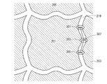
本実施の形態では、画素電極の構造として、図1と異なる一例を示す。
本実施の形態では、表示装置の構造の一例を説明する。
本実施の形態では、表示装置の作製方法の一例を説明する。なお、材料や構造などは、上記実施の形態で示す構成を適宜用いることができる。
本実施の形態では、表示装置の作製方法について、実施の形態4と異なる一例を示す。なお、材料や構造などは、上記実施の形態で示す構成を適宜用いることができる。
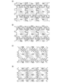
本実施の形態では、画素電極と他の配線との位置関係について説明する。
本実施の形態では、電子機器の一例を説明する。
103 部分
104 部分
105 部分
211 凹部
215 凹部
213 凸部
217 凸部
201 画素電極
203 画素電極
205 画素電極
219 隙間
221 隙間
301 部分
303 部分
305 部分
307 頂点
401 端部
403 端部
501 端部
502 端部
503 端部
504 端部
505 部分
507 部分
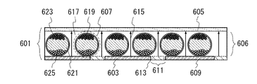
601 表示素子
603 画素電極
605 対向電極
606 帯電層
607 マイクロカプセル
609 画素電極
611 隙間
613 部分
615 矢印
617 樹脂
619 膜
621 液体
623 粒子
625 粒子
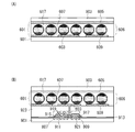
701 画素電極
703 画素電極
705 画素電極
707 画素電極
801 画素
803 配線
805 配線
807 トランジスタ
809 容量素子
811 駆動回路
813 駆動回路
901 基板
903 対向基板
911 電極
915 電極
917 電極
921 電極
913 絶縁膜
923 絶縁膜
919 半導体層
931 剥離層
933 絶縁膜
935 絶縁膜
937 溝
939 セパレートフィルム
941 第1の有機樹脂
943 素子層
945 第2の有機樹脂
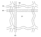
950 隙間
960 隙間
4001〜4006 本体
4101〜4106 表示部
5001 画素電極
5003 端部
5005 隙間
Claims (1)
- 複数の画素電極と、前記画素電極の上方の帯電層とを有し、
前記複数の画素電極のうち隣接する2つの画素電極の間には、隙間が形成されており、
前記隙間は、前記画素電極の一辺に渡り間隔が等しくなるように設けられており、
前記隣接する2つの画素電極のうちの一方は、端面方向に台形状に突出する部分を有し、
前記帯電層に電界を印加して表示を行う機能を有することを特徴とする表示装置。
Priority Applications (1)
| Application Number | Priority Date | Filing Date | Title |
|---|---|---|---|
| JP2011136107A JP6126775B2 (ja) | 2010-06-25 | 2011-06-20 | 表示装置 |
Applications Claiming Priority (3)
| Application Number | Priority Date | Filing Date | Title |
|---|---|---|---|
| JP2010144911 | 2010-06-25 | ||
| JP2010144911 | 2010-06-25 | ||
| JP2011136107A JP6126775B2 (ja) | 2010-06-25 | 2011-06-20 | 表示装置 |
Related Child Applications (1)
| Application Number | Title | Priority Date | Filing Date |
|---|---|---|---|
| JP2015213778A Division JP2016014907A (ja) | 2010-06-25 | 2015-10-30 | 表示装置の作製方法 |
Publications (3)
| Publication Number | Publication Date |
|---|---|
| JP2012027456A JP2012027456A (ja) | 2012-02-09 |
| JP2012027456A5 JP2012027456A5 (ja) | 2014-07-31 |
| JP6126775B2 true JP6126775B2 (ja) | 2017-05-10 |
Family
ID=45352319
Family Applications (6)
| Application Number | Title | Priority Date | Filing Date |
|---|---|---|---|
| JP2011136107A Active JP6126775B2 (ja) | 2010-06-25 | 2011-06-20 | 表示装置 |
| JP2015213778A Withdrawn JP2016014907A (ja) | 2010-06-25 | 2015-10-30 | 表示装置の作製方法 |
| JP2017168253A Active JP6460606B2 (ja) | 2010-06-25 | 2017-09-01 | 表示装置 |
| JP2018240426A Active JP6797887B2 (ja) | 2010-06-25 | 2018-12-24 | 表示装置 |
| JP2020191420A Active JP7142076B2 (ja) | 2010-06-25 | 2020-11-18 | 表示装置 |
| JP2022144509A Active JP7266741B2 (ja) | 2010-06-25 | 2022-09-12 | 表示装置 |
Family Applications After (5)
| Application Number | Title | Priority Date | Filing Date |
|---|---|---|---|
| JP2015213778A Withdrawn JP2016014907A (ja) | 2010-06-25 | 2015-10-30 | 表示装置の作製方法 |
| JP2017168253A Active JP6460606B2 (ja) | 2010-06-25 | 2017-09-01 | 表示装置 |
| JP2018240426A Active JP6797887B2 (ja) | 2010-06-25 | 2018-12-24 | 表示装置 |
| JP2020191420A Active JP7142076B2 (ja) | 2010-06-25 | 2020-11-18 | 表示装置 |
| JP2022144509A Active JP7266741B2 (ja) | 2010-06-25 | 2022-09-12 | 表示装置 |
Country Status (3)
| Country | Link |
|---|---|
| US (6) | US8786934B2 (ja) |
| JP (6) | JP6126775B2 (ja) |
| TW (7) | TWI635346B (ja) |
Families Citing this family (6)
| Publication number | Priority date | Publication date | Assignee | Title |
|---|---|---|---|---|
| JP6126775B2 (ja) * | 2010-06-25 | 2017-05-10 | 株式会社半導体エネルギー研究所 | 表示装置 |
| KR102491853B1 (ko) * | 2015-12-09 | 2023-01-26 | 삼성전자주식회사 | 지향성 백라이트 유닛 및 이를 포함한 입체 영상 표시 장치 |
| WO2017184816A1 (en) * | 2016-04-22 | 2017-10-26 | E Ink Corporation | Foldable electro-optic display apparatus |
| CN109581769A (zh) * | 2018-12-11 | 2019-04-05 | 合肥鑫晟光电科技有限公司 | 像素结构、阵列基板及显示面板 |
| JP2021044278A (ja) * | 2019-09-06 | 2021-03-18 | キオクシア株式会社 | 半導体装置 |
| CN112037679A (zh) * | 2020-08-12 | 2020-12-04 | 北京纳米能源与系统研究所 | 一种电子画板及显示方法 |
Family Cites Families (63)
| Publication number | Priority date | Publication date | Assignee | Title |
|---|---|---|---|---|
| JP3096202B2 (ja) | 1994-01-31 | 2000-10-10 | ポリプラスチックス株式会社 | トリオキサンの製造方法 |
| JP3774855B2 (ja) | 1997-04-25 | 2006-05-17 | 大林精工株式会社 | 液晶表示装置と製造方法. |
| EP1103840B1 (en) | 1997-06-12 | 2008-08-13 | Sharp Kabushiki Kaisha | Vertically-aligned (va) liquid crystal display device |
| JPH11174481A (ja) * | 1997-12-05 | 1999-07-02 | San Operation Service:Kk | 表示装置 |
| JPH11174453A (ja) * | 1997-12-16 | 1999-07-02 | Fujitsu Ltd | 液晶表示装置 |
| US6630977B1 (en) | 1999-05-20 | 2003-10-07 | Semiconductor Energy Laboratory Co., Ltd. | Semiconductor device with capacitor formed around contact hole |
| JP3982137B2 (ja) * | 2000-02-09 | 2007-09-26 | セイコーエプソン株式会社 | 電気光学装置および投射型表示装置 |
| TW583425B (en) | 2001-08-02 | 2004-04-11 | Sanyo Electric Co | Liquid crystal display |
| JP4785300B2 (ja) | 2001-09-07 | 2011-10-05 | 株式会社半導体エネルギー研究所 | 電気泳動型表示装置、表示装置、及び電子機器 |
| JP2003149674A (ja) | 2001-11-13 | 2003-05-21 | Hitachi Ltd | 液晶表示装置 |
| US6885146B2 (en) | 2002-03-14 | 2005-04-26 | Semiconductor Energy Laboratory Co., Ltd. | Display device comprising substrates, contrast medium and barrier layers between contrast medium and each of substrates |
| TWI240842B (en) | 2002-04-24 | 2005-10-01 | Sipix Imaging Inc | Matrix driven electrophoretic display with multilayer back plane |
| WO2003092077A2 (en) | 2002-04-24 | 2003-11-06 | E Ink Corporation | Electronic displays |
| US7190008B2 (en) | 2002-04-24 | 2007-03-13 | E Ink Corporation | Electro-optic displays, and components for use therein |
| TW588182B (en) | 2002-06-07 | 2004-05-21 | Hannstar Display Corp | Pixel electrode for a liquid crystal display with a high aperture ratio |
| WO2004105054A1 (ja) | 2003-05-20 | 2004-12-02 | Idemitsu Kosan Co. Ltd. | 非晶質透明導電膜、及びその原料スパッタリングターゲット、及び非晶質透明電極基板、及びその製造方法、及び液晶ディスプレイ用カラーフィルタ |
| KR20050014414A (ko) * | 2003-07-31 | 2005-02-07 | 삼성전자주식회사 | 다중 도메인 액정 표시 장치 |
| KR101100874B1 (ko) * | 2003-10-08 | 2012-01-02 | 삼성전자주식회사 | 박막 트랜지스터 표시판 |
| WO2005045509A2 (en) | 2003-10-27 | 2005-05-19 | E Ink Corporation | Electro-optic displays |
| CN100451784C (zh) * | 2004-01-29 | 2009-01-14 | 夏普株式会社 | 显示装置 |
| KR100781819B1 (ko) | 2004-03-19 | 2007-12-03 | 도꾸리쯔교세이호징 가가꾸 기쥬쯔 신꼬 기꼬 | 액정표시 소자 |
| US7573551B2 (en) | 2004-05-21 | 2009-08-11 | Sanyo Electric Co., Ltd. | Transflective liquid crystal display device and color liquid crystal display device |
| TWI349139B (en) * | 2004-11-30 | 2011-09-21 | Sanyo Electric Co | Liquid crystal display device |
| JP4748440B2 (ja) * | 2005-03-03 | 2011-08-17 | セイコーエプソン株式会社 | 電気泳動表示装置および電子機器 |
| JP2006259383A (ja) * | 2005-03-17 | 2006-09-28 | Seiko Epson Corp | 電子デバイス用基板の製造方法、電子デバイス用基板、電子デバイスおよび電子機器 |
| TWM274548U (en) * | 2005-03-18 | 2005-09-01 | Innolux Display Corp | Liquid crystal display device |
| KR101201017B1 (ko) | 2005-06-27 | 2012-11-13 | 엘지디스플레이 주식회사 | 액정 표시 장치 및 그 제조 방법 |
| JP2007010824A (ja) | 2005-06-29 | 2007-01-18 | Mitsubishi Electric Corp | 液晶ディスプレイパネル及びその画素欠陥修正方法 |
| KR101225440B1 (ko) | 2005-06-30 | 2013-01-25 | 엘지디스플레이 주식회사 | 액정 표시 장치 및 그 제조 방법 |
| JP4746933B2 (ja) * | 2005-08-01 | 2011-08-10 | Nec液晶テクノロジー株式会社 | カラー電子ペーパー表示装置 |
| TWI483048B (zh) | 2005-10-18 | 2015-05-01 | Semiconductor Energy Lab | 液晶顯示裝置 |
| JP2007133013A (ja) * | 2005-11-08 | 2007-05-31 | Canon Inc | 粒子移動型表示装置 |
| US7847904B2 (en) | 2006-06-02 | 2010-12-07 | Semiconductor Energy Laboratory Co., Ltd. | Liquid crystal display device and electronic appliance |
| JP2008058690A (ja) * | 2006-08-31 | 2008-03-13 | Seiko Epson Corp | 液晶装置、及び電子機器 |
| CN103257491B (zh) | 2006-09-29 | 2017-04-19 | 株式会社半导体能源研究所 | 半导体设备 |
| US8223287B2 (en) * | 2006-10-11 | 2012-07-17 | Seiko Epson Corporation | Electrooptic device and electronic device |
| JP2008096616A (ja) * | 2006-10-11 | 2008-04-24 | Seiko Epson Corp | 電気光学装置及び電子機器 |
| US8531991B2 (en) * | 2006-10-16 | 2013-09-10 | Cisco Technology, Inc. | Multi-chassis emulated switch |
| JP5119645B2 (ja) * | 2006-10-20 | 2013-01-16 | セイコーエプソン株式会社 | 電気光学装置、及びこれを備えた電子機器 |
| KR20080051273A (ko) * | 2006-12-05 | 2008-06-11 | 삼성전자주식회사 | 전기 영동 표시 장치 및 그 제조 방법 |
| JP2008159934A (ja) * | 2006-12-25 | 2008-07-10 | Kyodo Printing Co Ltd | フレキシブルtft基板及びその製造方法とフレキシブルディスプレイ |
| JP5075420B2 (ja) | 2007-02-09 | 2012-11-21 | 株式会社東芝 | 液晶表示装置 |
| JP2008292997A (ja) | 2007-04-27 | 2008-12-04 | Semiconductor Energy Lab Co Ltd | 液晶表示装置の作製方法 |
| TWI431386B (zh) | 2007-05-01 | 2014-03-21 | Prime View Int Co Ltd | 電子墨水顯示面板 |
| JP2009003437A (ja) | 2007-05-18 | 2009-01-08 | Semiconductor Energy Lab Co Ltd | 液晶表示装置およびその作製方法 |
| JP5218959B2 (ja) | 2007-06-01 | 2013-06-26 | 株式会社リコー | 電気泳動表示装置、表示方法、電気泳動表示素子の製造方法、及び電気泳動表示装置の製造方法 |
| US7968388B2 (en) | 2007-08-31 | 2011-06-28 | Seiko Epson Corporation | Thin-film device, method for manufacturing thin-film device, and display |
| JP2009076852A (ja) | 2007-08-31 | 2009-04-09 | Seiko Epson Corp | 薄膜素子、薄膜素子の製造方法、及び表示装置 |
| KR101346921B1 (ko) * | 2008-02-19 | 2014-01-02 | 엘지디스플레이 주식회사 | 평판 표시 장치 및 그 제조방법 |
| KR101445332B1 (ko) * | 2008-02-19 | 2014-10-01 | 삼성디스플레이 주식회사 | 표시장치 |
| JP5540517B2 (ja) | 2008-02-22 | 2014-07-02 | 凸版印刷株式会社 | 画像表示装置 |
| JP5266815B2 (ja) | 2008-03-14 | 2013-08-21 | セイコーエプソン株式会社 | 電気泳動表示装置及び電子機器 |
| JP5358324B2 (ja) | 2008-07-10 | 2013-12-04 | 株式会社半導体エネルギー研究所 | 電子ペーパー |
| TW201023021A (en) * | 2008-12-03 | 2010-06-16 | Chi Hsin Electronics Corp | Touch sensitive electronic paper display apparatus |
| KR101283366B1 (ko) | 2008-12-23 | 2013-07-08 | 엘지디스플레이 주식회사 | 전기영동 표시장치용 어레이 기판 및 그 제조 방법 |
| WO2010128616A1 (en) | 2009-05-02 | 2010-11-11 | Semiconductor Energy Laboratory Co., Ltd. | Electronic book |
| KR101643835B1 (ko) | 2009-07-10 | 2016-07-28 | 가부시키가이샤 한도오따이 에네루기 켄큐쇼 | 반도체 장치 및 그 제조 방법 |
| WO2011010545A1 (en) | 2009-07-18 | 2011-01-27 | Semiconductor Energy Laboratory Co., Ltd. | Semiconductor device and method for manufacturing the same |
| KR101785992B1 (ko) | 2009-07-24 | 2017-10-18 | 가부시키가이샤 한도오따이 에네루기 켄큐쇼 | 반도체 장치 |
| JP4930561B2 (ja) * | 2009-09-07 | 2012-05-16 | カシオ計算機株式会社 | 電気泳動表示パネル |
| TWI528342B (zh) | 2009-09-16 | 2016-04-01 | 半導體能源研究所股份有限公司 | 顯示裝置及其驅動方法 |
| JP6126775B2 (ja) * | 2010-06-25 | 2017-05-10 | 株式会社半導体エネルギー研究所 | 表示装置 |
| JP5947000B2 (ja) * | 2010-07-01 | 2016-07-06 | 株式会社半導体エネルギー研究所 | 電界駆動型表示装置 |
-
2011
- 2011-06-20 JP JP2011136107A patent/JP6126775B2/ja active Active
- 2011-06-21 TW TW106118888A patent/TWI635346B/zh active
- 2011-06-21 TW TW105134061A patent/TWI596415B/zh active
- 2011-06-21 TW TW109124242A patent/TWI742766B/zh active
- 2011-06-21 TW TW107121155A patent/TWI701491B/zh active
- 2011-06-21 TW TW100121639A patent/TWI515500B/zh active
- 2011-06-21 TW TW104134020A patent/TWI567470B/zh active
- 2011-06-21 TW TW110135318A patent/TWI802020B/zh active
- 2011-06-24 US US13/168,025 patent/US8786934B2/en active Active
-
2014
- 2014-07-18 US US14/335,306 patent/US8958140B2/en active Active
-
2015
- 2015-02-10 US US14/618,418 patent/US9268193B2/en active Active
- 2015-10-30 JP JP2015213778A patent/JP2016014907A/ja not_active Withdrawn
-
2016
- 2016-02-17 US US15/046,207 patent/US9488895B2/en active Active
- 2016-11-02 US US15/341,874 patent/US9857658B2/en active Active
-
2017
- 2017-09-01 JP JP2017168253A patent/JP6460606B2/ja active Active
- 2017-12-27 US US15/855,167 patent/US10185201B2/en active Active
-
2018
- 2018-12-24 JP JP2018240426A patent/JP6797887B2/ja active Active
-
2020
- 2020-11-18 JP JP2020191420A patent/JP7142076B2/ja active Active
-
2022
- 2022-09-12 JP JP2022144509A patent/JP7266741B2/ja active Active
Also Published As
Similar Documents
| Publication | Publication Date | Title |
|---|---|---|
| JP6460606B2 (ja) | 表示装置 | |
| US20100265565A1 (en) | Display Device with Improved Display Performance | |
| KR101993592B1 (ko) | 표시 장치 | |
| JP7478284B2 (ja) | 表示装置 | |
| JP6364810B2 (ja) | 電気光学装置、電気光学装置の製造方法 |
Legal Events
| Date | Code | Title | Description |
|---|---|---|---|
| A521 | Request for written amendment filed |
Free format text: JAPANESE INTERMEDIATE CODE: A523 Effective date: 20140617 |
|
| A621 | Written request for application examination |
Free format text: JAPANESE INTERMEDIATE CODE: A621 Effective date: 20140617 |
|
| A131 | Notification of reasons for refusal |
Free format text: JAPANESE INTERMEDIATE CODE: A131 Effective date: 20150519 |
|
| A521 | Request for written amendment filed |
Free format text: JAPANESE INTERMEDIATE CODE: A523 Effective date: 20150617 |
|
| A02 | Decision of refusal |
Free format text: JAPANESE INTERMEDIATE CODE: A02 Effective date: 20150818 |
|
| A521 | Request for written amendment filed |
Free format text: JAPANESE INTERMEDIATE CODE: A523 Effective date: 20151030 |
|
| A911 | Transfer to examiner for re-examination before appeal (zenchi) |
Free format text: JAPANESE INTERMEDIATE CODE: A911 Effective date: 20151109 |
|
| A912 | Re-examination (zenchi) completed and case transferred to appeal board |
Free format text: JAPANESE INTERMEDIATE CODE: A912 Effective date: 20151218 |
|
| A61 | First payment of annual fees (during grant procedure) |
Free format text: JAPANESE INTERMEDIATE CODE: A61 Effective date: 20170410 |
|
| R150 | Certificate of patent or registration of utility model |
Ref document number: 6126775 Country of ref document: JP Free format text: JAPANESE INTERMEDIATE CODE: R150 |
|
| R250 | Receipt of annual fees |
Free format text: JAPANESE INTERMEDIATE CODE: R250 |
|
| R250 | Receipt of annual fees |
Free format text: JAPANESE INTERMEDIATE CODE: R250 |
|
| R250 | Receipt of annual fees |
Free format text: JAPANESE INTERMEDIATE CODE: R250 |
|
| R250 | Receipt of annual fees |
Free format text: JAPANESE INTERMEDIATE CODE: R250 |
|
| R250 | Receipt of annual fees |
Free format text: JAPANESE INTERMEDIATE CODE: R250 |