JP6058351B2 - 光源モジュール及びこれを備えた照明装置 - Google Patents
光源モジュール及びこれを備えた照明装置 Download PDFInfo
- Publication number
- JP6058351B2 JP6058351B2 JP2012237127A JP2012237127A JP6058351B2 JP 6058351 B2 JP6058351 B2 JP 6058351B2 JP 2012237127 A JP2012237127 A JP 2012237127A JP 2012237127 A JP2012237127 A JP 2012237127A JP 6058351 B2 JP6058351 B2 JP 6058351B2
- Authority
- JP
- Japan
- Prior art keywords
- light
- light source
- source module
- light emitting
- polymer layer
- Prior art date
- Legal status (The legal status is an assumption and is not a legal conclusion. Google has not performed a legal analysis and makes no representation as to the accuracy of the status listed.)
- Expired - Fee Related
Links
Images


Classifications
-
- H—ELECTRICITY
- H01—ELECTRIC ELEMENTS
- H01L—SEMICONDUCTOR DEVICES NOT COVERED BY CLASS H10
- H01L33/00—Semiconductor devices with at least one potential-jump barrier or surface barrier specially adapted for light emission; Processes or apparatus specially adapted for the manufacture or treatment thereof or of parts thereof; Details thereof
- H01L33/48—Semiconductor devices with at least one potential-jump barrier or surface barrier specially adapted for light emission; Processes or apparatus specially adapted for the manufacture or treatment thereof or of parts thereof; Details thereof characterised by the semiconductor body packages
- H01L33/58—Optical field-shaping elements
-
- H—ELECTRICITY
- H01—ELECTRIC ELEMENTS
- H01L—SEMICONDUCTOR DEVICES NOT COVERED BY CLASS H10
- H01L33/00—Semiconductor devices with at least one potential-jump barrier or surface barrier specially adapted for light emission; Processes or apparatus specially adapted for the manufacture or treatment thereof or of parts thereof; Details thereof
- H01L33/48—Semiconductor devices with at least one potential-jump barrier or surface barrier specially adapted for light emission; Processes or apparatus specially adapted for the manufacture or treatment thereof or of parts thereof; Details thereof characterised by the semiconductor body packages
- H01L33/52—Encapsulations
-
- H—ELECTRICITY
- H01—ELECTRIC ELEMENTS
- H01L—SEMICONDUCTOR DEVICES NOT COVERED BY CLASS H10
- H01L2224/00—Indexing scheme for arrangements for connecting or disconnecting semiconductor or solid-state bodies and methods related thereto as covered by H01L24/00
- H01L2224/01—Means for bonding being attached to, or being formed on, the surface to be connected, e.g. chip-to-package, die-attach, "first-level" interconnects; Manufacturing methods related thereto
- H01L2224/42—Wire connectors; Manufacturing methods related thereto
- H01L2224/47—Structure, shape, material or disposition of the wire connectors after the connecting process
- H01L2224/48—Structure, shape, material or disposition of the wire connectors after the connecting process of an individual wire connector
- H01L2224/4805—Shape
- H01L2224/4809—Loop shape
- H01L2224/48091—Arched
-
- H—ELECTRICITY
- H01—ELECTRIC ELEMENTS
- H01L—SEMICONDUCTOR DEVICES NOT COVERED BY CLASS H10
- H01L2224/00—Indexing scheme for arrangements for connecting or disconnecting semiconductor or solid-state bodies and methods related thereto as covered by H01L24/00
- H01L2224/01—Means for bonding being attached to, or being formed on, the surface to be connected, e.g. chip-to-package, die-attach, "first-level" interconnects; Manufacturing methods related thereto
- H01L2224/42—Wire connectors; Manufacturing methods related thereto
- H01L2224/47—Structure, shape, material or disposition of the wire connectors after the connecting process
- H01L2224/48—Structure, shape, material or disposition of the wire connectors after the connecting process of an individual wire connector
- H01L2224/481—Disposition
- H01L2224/48151—Connecting between a semiconductor or solid-state body and an item not being a semiconductor or solid-state body, e.g. chip-to-substrate, chip-to-passive
- H01L2224/48221—Connecting between a semiconductor or solid-state body and an item not being a semiconductor or solid-state body, e.g. chip-to-substrate, chip-to-passive the body and the item being stacked
- H01L2224/48245—Connecting between a semiconductor or solid-state body and an item not being a semiconductor or solid-state body, e.g. chip-to-substrate, chip-to-passive the body and the item being stacked the item being metallic
- H01L2224/48247—Connecting between a semiconductor or solid-state body and an item not being a semiconductor or solid-state body, e.g. chip-to-substrate, chip-to-passive the body and the item being stacked the item being metallic connecting the wire to a bond pad of the item
-
- H—ELECTRICITY
- H01—ELECTRIC ELEMENTS
- H01L—SEMICONDUCTOR DEVICES NOT COVERED BY CLASS H10
- H01L2924/00—Indexing scheme for arrangements or methods for connecting or disconnecting semiconductor or solid-state bodies as covered by H01L24/00
- H01L2924/10—Details of semiconductor or other solid state devices to be connected
- H01L2924/11—Device type
- H01L2924/13—Discrete devices, e.g. 3 terminal devices
- H01L2924/1301—Thyristor
Description
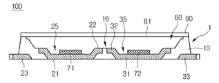
60 凹部
10、131 胴体
25、35、135 キャビティー
21、31、112、113 リードフレーム
46 連結フレーム
71、72 発光チップ
90、90A、90B 光学的制御手段
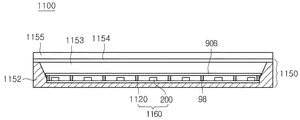
98 サポーター
100、101 光源モジュール
1120、1033 基板
1031、1160 発光モジュール
Claims (15)
- 凹部を有する胴体と、
前記凹部の第1領域の下に配置された、第1キャビティーを有する第1リードフレームと、
前記凹部の第2領域の下に配置された、第2キャビティーを有する第2リードフレームと、
前記第1リードフレームの前記第1キャビティーに配置された第1発光チップと、
前記第2リードフレームの前記第2キャビティーに配置された第2発光チップと、
前記凹部並びに前記第1及び第2キャビティーにモールディング部材と、
前記胴体の上に配置され、前記第1及び第2発光チップから放出された光を屈折させる高分子層と、
前記高分子層の上に配置され、入射される光を放出する第1電極層と、
前記高分子層と前記胴体との間に配置され、前記第1及び第2発光チップから放出された光が透過される第2電極層と、
前記第1電極層の上に配置された第1ベースフィルムと、
前記第2電極層の下に配置された第2ベースフィルムと、
を備え、
前記第2ベースフィルムの一部は、前記モールディング部材の上面に接触し、
前記第2ベースフィルムは、前記胴体の上面に接着され、
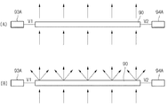
前記モールディング部材と前記第2ベースフィルムとの間に拡散層を有することを特徴とする、光源モジュール。 - 前記高分子層は前記第1電極層と前記第2電極層に供給される電圧の差によって前記第1電極層から入射される光の指向角を変換させることを特徴とする、請求項1に記載の光源モジュール。
- 前記高分子層は液晶を含むことを特徴とする、請求項1または2に記載の光源モジュール。
- 前記液晶は0.15乃至0.25の範囲の屈折率異方性を有することを特徴とする、請求項3に記載の光源モジュール。
- 前記拡散層は、内部に拡散剤を有し、
前記第2ベースフィルムは、前記第1及び第2発光チップから4mm以下の間隔を有することを特徴とする、請求項1乃至4のいずれか1項に記載の光源モジュール。 - 前記高分子層の下面の面積は、前記胴体の下面の面積の90%乃至150%の範囲を有することを特徴とする、請求項1乃至5のいずれか1項に記載の光源モジュール。
- 前記第1及び第2ベースフィルムは透光性フィルムであることを特徴とする、請求項1乃至6のいずれか1項に記載の光源モジュール。
- 前記第1及び第2電極層は透光性の金属酸化物または金属窒化物を含むことを特徴とする、請求項1乃至7のいずれか1項に記載の光源モジュール。
- 前記高分子層の幅は、前記胴体の下面の幅の90%乃至150%の範囲を有することを特徴とする、請求項1乃至8のいずれか1項に記載の光源モジュール。
- 前記胴体の上面コーナーに突出された複数のガイド部を含み、
前記高分子層、前記第1及び第2電極層並びに前記第1及び第2ベースフィルムは、隅部分がカッティングされ、前記ガイド部に対応する結合部を有することを特徴とする、請求項1乃至9のいずれか1項に記載の光源モジュール。 - 前記高分子層は前記第1及び第2電極層の電圧によって前記第1及び第2発光チップから放出された光を遮断または透過させることを特徴とする、請求項1乃至10のいずれか1項に記載の光源モジュール。
- 前記第1及び第2電極層は前記胴体の幅より広い幅を有することを特徴とする、請求項1乃至11のいずれか1項に記載の光源モジュール。
- 前記高分子層は前記第1及び第2電極層に供給される第1駆動電圧と第2駆動電圧との差が前記第1駆動電圧を基準に70%を超過すれば、入射される光を130度以下の光指向角分布で照射することを特徴とする、請求項1乃至12のいずれか1項に記載の光源モジュール。
- 前記高分子層は前記第1及び第2電極層に供給される第1駆動電圧と第2駆動電圧との差が前記第1駆動電圧を基準に30%乃至70%範囲の差が出れば、入射される光を140度以上の光指向角分布で照射することを特徴とする、請求項1乃至13のいずれか1項に記載の光源モジュール。
- 前記胴体の上面の周りに収納溝を含み、
前記収納溝には、前記第2ベースフィルム及び前記第2電極層の外側縁部が配置され、
前記収納溝にコネクターが配置されるコネクター溝を有することを特徴とする、請求項1乃至8のいずれか1項に記載の光源モジュール。
Applications Claiming Priority (2)
| Application Number | Priority Date | Filing Date | Title |
|---|---|---|---|
| KR10-2011-0110059 | 2011-10-26 | ||
| KR1020110110059A KR20130045687A (ko) | 2011-10-26 | 2011-10-26 | 발광 장치 및 이를 구비한 조명 장치 |
Publications (3)
| Publication Number | Publication Date |
|---|---|
| JP2013093583A JP2013093583A (ja) | 2013-05-16 |
| JP2013093583A5 JP2013093583A5 (ja) | 2015-12-10 |
| JP6058351B2 true JP6058351B2 (ja) | 2017-01-11 |
Family
ID=47602765
Family Applications (1)
| Application Number | Title | Priority Date | Filing Date |
|---|---|---|---|
| JP2012237127A Expired - Fee Related JP6058351B2 (ja) | 2011-10-26 | 2012-10-26 | 光源モジュール及びこれを備えた照明装置 |
Country Status (6)
| Country | Link |
|---|---|
| US (1) | US8842255B2 (ja) |
| EP (1) | EP2587561B1 (ja) |
| JP (1) | JP6058351B2 (ja) |
| KR (1) | KR20130045687A (ja) |
| CN (1) | CN103075678B (ja) |
| TW (1) | TWI562327B (ja) |
Families Citing this family (15)
| Publication number | Priority date | Publication date | Assignee | Title |
|---|---|---|---|---|
| KR102029867B1 (ko) * | 2013-08-08 | 2019-11-08 | 엘지이노텍 주식회사 | 발광소자 패키지 및 조명시스템 |
| CN103411164B (zh) * | 2013-08-19 | 2015-12-30 | 吴金香 | 一种可调节照明角度的路灯 |
| KR102131340B1 (ko) * | 2014-01-27 | 2020-07-07 | 엘지이노텍 주식회사 | 발광 소자 및 이를 구비한 조명 시스템 |
| KR102248084B1 (ko) * | 2014-08-06 | 2021-05-04 | 엘지이노텍 주식회사 | 발광소자 패키지 |
| KR101643862B1 (ko) * | 2015-02-24 | 2016-07-29 | 엘지전자 주식회사 | 발광소자 패키지 |
| KR102409180B1 (ko) * | 2015-07-15 | 2022-06-15 | 쑤저우 레킨 세미컨덕터 컴퍼니 리미티드 | 발광 소자 패키지 및 조명 장치 |
| DE102016103136A1 (de) * | 2016-02-23 | 2017-08-24 | Vishay Semiconductor Gmbh | Optoelektronische Vorrichtung |
| US10270020B2 (en) * | 2017-06-20 | 2019-04-23 | Lextar Electronics Corporation | LED package structure |
| JP7108892B2 (ja) * | 2018-04-25 | 2022-07-29 | パナソニックIpマネジメント株式会社 | 照明器具 |
| JP7054843B2 (ja) * | 2018-04-25 | 2022-04-15 | パナソニックIpマネジメント株式会社 | 照明器具 |
| KR102626250B1 (ko) * | 2018-08-31 | 2024-01-17 | 현대자동차주식회사 | 차량용 라이팅 장치 및 이의 이용 방법 |
| JP7370274B2 (ja) | 2020-02-18 | 2023-10-27 | 日機装株式会社 | 半導体パッケージ及び半導体発光装置 |
| CN113555490A (zh) * | 2020-04-26 | 2021-10-26 | 群创光电股份有限公司 | 发光装置 |
| KR20220065153A (ko) * | 2020-11-12 | 2022-05-20 | 삼성전자주식회사 | 광원 모듈 및 이를 포함하는 모바일 기기 |
| DE102021108349A1 (de) * | 2021-04-01 | 2022-10-06 | OSRAM Opto Semiconductors Gesellschaft mit beschränkter Haftung | Licht emittierende vorrichtung und lidar-system |
Family Cites Families (23)
| Publication number | Priority date | Publication date | Assignee | Title |
|---|---|---|---|---|
| JP2004240259A (ja) * | 2003-02-07 | 2004-08-26 | Sharp Corp | 液晶調光デバイス及び液晶表示装置 |
| JP4471729B2 (ja) * | 2004-04-30 | 2010-06-02 | シチズン電子株式会社 | 液晶レンズ付き発光装置 |
| WO2006098450A1 (ja) * | 2005-03-18 | 2006-09-21 | Mitsubishi Chemical Corporation | 発光装置、白色発光装置、照明装置及び画像表示装置 |
| CN101442097B (zh) * | 2005-03-18 | 2010-11-10 | 三菱化学株式会社 | 发光装置、白光发光装置、照明装置及图像显示装置 |
| JP4508048B2 (ja) * | 2005-09-02 | 2010-07-21 | 旭硝子株式会社 | 液晶レンズおよび光ヘッド装置 |
| JP2007095998A (ja) * | 2005-09-29 | 2007-04-12 | Harison Toshiba Lighting Corp | 発光装置 |
| JP2007134656A (ja) * | 2005-11-14 | 2007-05-31 | Toyoda Gosei Co Ltd | 蛍光体板及びこれを備えた発光装置 |
| JP2007180127A (ja) * | 2005-12-27 | 2007-07-12 | Nikon Corp | 光学素子モジュール及びその光学素子モジュールを備える電子部品 |
| CN101371073B (zh) * | 2006-01-16 | 2010-06-09 | 皇家飞利浦电子股份有限公司 | 灯模块和包括这种灯模块的照明器件 |
| TW200813557A (en) * | 2006-09-12 | 2008-03-16 | Kenmos Technology Co Ltd | Liquid crystal display device |
| DE102007010244A1 (de) * | 2007-02-02 | 2008-08-07 | Osram Opto Semiconductors Gmbh | Anordnung und Verfahren zur Erzeugung von Mischlicht |
| JP2008281600A (ja) * | 2007-05-08 | 2008-11-20 | Citizen Electronics Co Ltd | ズームレンズ付きカメラの補助光装置及び、その補助光装置を備えたズームレンズ付きカメラ、及びその補助光装置に用いる拡散率可変led。 |
| US20090026470A1 (en) * | 2007-07-23 | 2009-01-29 | Novalite Optronics Corp. | Super thin side-view light-emitting diode (led) package and fabrication method thereof |
| JP2009151140A (ja) * | 2007-12-21 | 2009-07-09 | Panasonic Corp | 液晶フレネルレンズ及び、その製造方法 |
| JP5459685B2 (ja) * | 2008-09-23 | 2014-04-02 | コーニンクレッカ フィリップス エヌ ヴェ | 熱的に変化する反射素子を備えた照明デバイス |
| JP5431706B2 (ja) * | 2008-10-01 | 2014-03-05 | ミネベア株式会社 | 発光装置 |
| WO2011030578A1 (ja) * | 2009-09-11 | 2011-03-17 | Kataoka Shoei | Led照明装置 |
| TWI403808B (zh) * | 2009-10-27 | 2013-08-01 | Taiwan Tft Lcd Ass | 液晶顯示面板的製造方法 |
| JP5393802B2 (ja) * | 2009-10-29 | 2014-01-22 | 京セラ株式会社 | 発光装置 |
| KR101028313B1 (ko) * | 2009-12-03 | 2011-04-11 | 엘지이노텍 주식회사 | 발광 장치 및 그 제조 방법 |
| TWI398700B (zh) * | 2009-12-30 | 2013-06-11 | Au Optronics Corp | 使用量子點螢光粉之顯示裝置及其製造方法 |
| EP2346100B1 (en) * | 2010-01-15 | 2019-05-22 | LG Innotek Co., Ltd. | Light emitting apparatus and lighting system |
| EP2365552A3 (en) * | 2010-03-09 | 2015-03-25 | LG Innotek Co., Ltd. | Light emitting device package with a lead frame having a recess |
-
2011
- 2011-10-26 KR KR1020110110059A patent/KR20130045687A/ko not_active Application Discontinuation
-
2012
- 2012-10-22 US US13/657,194 patent/US8842255B2/en active Active
- 2012-10-23 TW TW101139091A patent/TWI562327B/zh active
- 2012-10-23 EP EP12189526.2A patent/EP2587561B1/en active Active
- 2012-10-26 CN CN201210417128.9A patent/CN103075678B/zh active Active
- 2012-10-26 JP JP2012237127A patent/JP6058351B2/ja not_active Expired - Fee Related
Also Published As
| Publication number | Publication date |
|---|---|
| CN103075678A (zh) | 2013-05-01 |
| TWI562327B (en) | 2016-12-11 |
| TW201324738A (zh) | 2013-06-16 |
| JP2013093583A (ja) | 2013-05-16 |
| EP2587561A2 (en) | 2013-05-01 |
| EP2587561A3 (en) | 2015-07-08 |
| US20130107169A1 (en) | 2013-05-02 |
| EP2587561B1 (en) | 2019-07-03 |
| US8842255B2 (en) | 2014-09-23 |
| KR20130045687A (ko) | 2013-05-06 |
| CN103075678B (zh) | 2017-07-04 |
Similar Documents
| Publication | Publication Date | Title |
|---|---|---|
| JP6058351B2 (ja) | 光源モジュール及びこれを備えた照明装置 | |
| JP5906038B2 (ja) | 発光素子 | |
| KR101655463B1 (ko) | 발광소자 패키지 및 이를 구비한 라이트 유닛 | |
| KR101997244B1 (ko) | 광원 모듈 및 이를 구비한 조명시스템 | |
| KR20130038065A (ko) | 발광 소자 패키지 및 이를 구비한 백라이트 유닛 | |
| KR20110128693A (ko) | 발광 소자 패키지 및 이를 구비한 라이트 유닛 | |
| KR101952438B1 (ko) | 발광소자 패키지 및 이를 구비한 라이트 유닛 | |
| KR20130022643A (ko) | 발광 소자 | |
| KR101559038B1 (ko) | 발광소자 패키지 및 이를 구비한 라이트 유닛 | |
| KR101724699B1 (ko) | 발광 장치 및 조명 시스템 | |
| KR102110477B1 (ko) | 발광 소자 및 이를 구비한 조명시스템 | |
| KR101924014B1 (ko) | 발광 소자 패키지 및 이를 구비한 조명 시스템 | |
| KR101997245B1 (ko) | 발광소자 패키지 | |
| KR102101367B1 (ko) | 발광 소자 | |
| KR101880058B1 (ko) | 발광 소자 패키지 및 조명 장치 | |
| KR101852553B1 (ko) | 발광소자 패키지 및 이를 구비한 라이트 유닛 | |
| KR102019830B1 (ko) | 발광소자 패키지 | |
| KR101905573B1 (ko) | 발광 모듈 및 이를 구비한 조명 시스템 | |
| KR101735310B1 (ko) | 발광소자 패키지 | |
| KR101916089B1 (ko) | 발광소자 패키지 및 이를 구비한 라이트 유닛 | |
| KR101946834B1 (ko) | 발광 소자 패키지 및 이를 구비한 라이트 유닛 | |
| KR101926468B1 (ko) | 발광 소자 패키지 | |
| KR101997249B1 (ko) | 발광 소자 | |
| KR20130072993A (ko) | 발광 소자 패키지 및 이를 구비한 조명 시스템 | |
| KR101724707B1 (ko) | 라이트 유닛 |
Legal Events
| Date | Code | Title | Description |
|---|---|---|---|
| A521 | Request for written amendment filed |
Free format text: JAPANESE INTERMEDIATE CODE: A523 Effective date: 20151022 |
|
| A621 | Written request for application examination |
Free format text: JAPANESE INTERMEDIATE CODE: A621 Effective date: 20151022 |
|
| A977 | Report on retrieval |
Free format text: JAPANESE INTERMEDIATE CODE: A971007 Effective date: 20160720 |
|
| A131 | Notification of reasons for refusal |
Free format text: JAPANESE INTERMEDIATE CODE: A131 Effective date: 20160726 |
|
| A521 | Request for written amendment filed |
Free format text: JAPANESE INTERMEDIATE CODE: A523 Effective date: 20161018 |
|
| TRDD | Decision of grant or rejection written | ||
| A01 | Written decision to grant a patent or to grant a registration (utility model) |
Free format text: JAPANESE INTERMEDIATE CODE: A01 Effective date: 20161122 |
|
| A61 | First payment of annual fees (during grant procedure) |
Free format text: JAPANESE INTERMEDIATE CODE: A61 Effective date: 20161207 |
|
| R150 | Certificate of patent or registration of utility model |
Ref document number: 6058351 Country of ref document: JP Free format text: JAPANESE INTERMEDIATE CODE: R150 |
|
| LAPS | Cancellation because of no payment of annual fees |