JP6028352B2 - ヒートシンク付パワーモジュール用基板の製造方法 - Google Patents
ヒートシンク付パワーモジュール用基板の製造方法 Download PDFInfo
- Publication number
- JP6028352B2 JP6028352B2 JP2012060687A JP2012060687A JP6028352B2 JP 6028352 B2 JP6028352 B2 JP 6028352B2 JP 2012060687 A JP2012060687 A JP 2012060687A JP 2012060687 A JP2012060687 A JP 2012060687A JP 6028352 B2 JP6028352 B2 JP 6028352B2
- Authority
- JP
- Japan
- Prior art keywords
- metal plate
- heat sink
- power module
- brazing
- ceramic substrate
- Prior art date
- Legal status (The legal status is an assumption and is not a legal conclusion. Google has not performed a legal analysis and makes no representation as to the accuracy of the status listed.)
- Active
Links
Images

Classifications
-
- H—ELECTRICITY
- H01—ELECTRIC ELEMENTS
- H01L—SEMICONDUCTOR DEVICES NOT COVERED BY CLASS H10
- H01L2224/00—Indexing scheme for arrangements for connecting or disconnecting semiconductor or solid-state bodies and methods related thereto as covered by H01L24/00
- H01L2224/01—Means for bonding being attached to, or being formed on, the surface to be connected, e.g. chip-to-package, die-attach, "first-level" interconnects; Manufacturing methods related thereto
- H01L2224/26—Layer connectors, e.g. plate connectors, solder or adhesive layers; Manufacturing methods related thereto
- H01L2224/31—Structure, shape, material or disposition of the layer connectors after the connecting process
- H01L2224/32—Structure, shape, material or disposition of the layer connectors after the connecting process of an individual layer connector
- H01L2224/321—Disposition
- H01L2224/32151—Disposition the layer connector connecting between a semiconductor or solid-state body and an item not being a semiconductor or solid-state body, e.g. chip-to-substrate, chip-to-passive
- H01L2224/32221—Disposition the layer connector connecting between a semiconductor or solid-state body and an item not being a semiconductor or solid-state body, e.g. chip-to-substrate, chip-to-passive the body and the item being stacked
- H01L2224/32225—Disposition the layer connector connecting between a semiconductor or solid-state body and an item not being a semiconductor or solid-state body, e.g. chip-to-substrate, chip-to-passive the body and the item being stacked the item being non-metallic, e.g. insulating substrate with or without metallisation
-
- H—ELECTRICITY
- H01—ELECTRIC ELEMENTS
- H01L—SEMICONDUCTOR DEVICES NOT COVERED BY CLASS H10
- H01L2224/00—Indexing scheme for arrangements for connecting or disconnecting semiconductor or solid-state bodies and methods related thereto as covered by H01L24/00
- H01L2224/01—Means for bonding being attached to, or being formed on, the surface to be connected, e.g. chip-to-package, die-attach, "first-level" interconnects; Manufacturing methods related thereto
- H01L2224/42—Wire connectors; Manufacturing methods related thereto
- H01L2224/47—Structure, shape, material or disposition of the wire connectors after the connecting process
- H01L2224/48—Structure, shape, material or disposition of the wire connectors after the connecting process of an individual wire connector
- H01L2224/4805—Shape
- H01L2224/4809—Loop shape
- H01L2224/48091—Arched
-
- H—ELECTRICITY
- H01—ELECTRIC ELEMENTS
- H01L—SEMICONDUCTOR DEVICES NOT COVERED BY CLASS H10
- H01L2224/00—Indexing scheme for arrangements for connecting or disconnecting semiconductor or solid-state bodies and methods related thereto as covered by H01L24/00
- H01L2224/01—Means for bonding being attached to, or being formed on, the surface to be connected, e.g. chip-to-package, die-attach, "first-level" interconnects; Manufacturing methods related thereto
- H01L2224/42—Wire connectors; Manufacturing methods related thereto
- H01L2224/47—Structure, shape, material or disposition of the wire connectors after the connecting process
- H01L2224/48—Structure, shape, material or disposition of the wire connectors after the connecting process of an individual wire connector
- H01L2224/481—Disposition
- H01L2224/48151—Connecting between a semiconductor or solid-state body and an item not being a semiconductor or solid-state body, e.g. chip-to-substrate, chip-to-passive
- H01L2224/48221—Connecting between a semiconductor or solid-state body and an item not being a semiconductor or solid-state body, e.g. chip-to-substrate, chip-to-passive the body and the item being stacked
- H01L2224/48225—Connecting between a semiconductor or solid-state body and an item not being a semiconductor or solid-state body, e.g. chip-to-substrate, chip-to-passive the body and the item being stacked the item being non-metallic, e.g. insulating substrate with or without metallisation
- H01L2224/48227—Connecting between a semiconductor or solid-state body and an item not being a semiconductor or solid-state body, e.g. chip-to-substrate, chip-to-passive the body and the item being stacked the item being non-metallic, e.g. insulating substrate with or without metallisation connecting the wire to a bond pad of the item
-
- H—ELECTRICITY
- H01—ELECTRIC ELEMENTS
- H01L—SEMICONDUCTOR DEVICES NOT COVERED BY CLASS H10
- H01L2224/00—Indexing scheme for arrangements for connecting or disconnecting semiconductor or solid-state bodies and methods related thereto as covered by H01L24/00
- H01L2224/73—Means for bonding being of different types provided for in two or more of groups H01L2224/10, H01L2224/18, H01L2224/26, H01L2224/34, H01L2224/42, H01L2224/50, H01L2224/63, H01L2224/71
- H01L2224/732—Location after the connecting process
- H01L2224/73251—Location after the connecting process on different surfaces
- H01L2224/73265—Layer and wire connectors
Description
パワーモジュール用基板の製造過程において、セラミックス基板と金属板とのろう付時に、接合に寄与しない余剰分のろう材が接合部から押し出され、金属板の側面に付着する場合がある。この一次ろう付工程で金属板側面に付着したろう材が固化し、金属板側面の表面に網目状の溝が形成され易く、このような状態で金属板とヒートシンクとをノコロックろう付すると、金属板とヒートシンクとの間から流出したフラックスが、金属板の側面に付着したろう材に接触し、この網目状の溝を伝って流動してセラミックス基板と金属板との接合部界面に引き込まれる。したがって、フラックスの侵食によるセラミックス基板と金属板との剥離を防止するには、このフラックスのろう材表面での流動を防止する必要がある。本発明は、このような知見の下、以下の解決手段とした。
金属板にろう材が付着していたとしても、その表面が算術平均粗さRaで0.7μm以下の平坦面であれば、ヒートシンクを接合する際にフラックスが金属板側面を伝ってセラミックス基板との接合部内に引き込まれることが防止される。
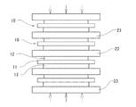
図1は、本実施形態のパワーモジュール用基板10を用いたパワーモジュール100を示している。このパワーモジュール100は、パワーモジュール用基板10と、パワーモジュール用基板10の表面に搭載された半導体チップ等の電子部品20と、この電子部品20とは反対面でパワーモジュール用基板10に接合されたヒートシンク30とから構成される。
具体的には、まず、金属板12,13を、シート材からプレス加工により形成する。この場合、回路層用金属板12は単にシート材から打ち抜くことにより形成される。一方、放熱層用金属板13は、シート材に複数の溝14を形成した後に打ち抜き加工される。溝14は、シート材の金属板13となる領域をカバーする範囲にパンチを押圧することにより形成される。
そして、これら積層したセラミックス基板11および各金属板12,13を厚さ方向に加圧しながら真空雰囲気中で加熱することによりろう付けする(一次ろう付工程)。
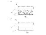
このとき、セラミックス基板11と金属板13との間からろう材が漏れ出ると、金属板13の側面13cに付着する。図3(a)は、その金属板13の側面13cにろう材が付着した状態を模式的に示しており、ろう材の表面に網目状の溝が形成される。
このブラスト研磨に際しては、金属板13の側面13c以外のパワーモジュール用基板10の表面(金属板13の溝14が形成されている面、セラミックス基板11の表面)をマスキングしておき、ノズルから圧縮空気とともに投射材(研磨材)を噴射して、金属板13の側面13cに吹き付ける。投射材としては例えば平均粒径28μm〜32μmのSiCの粉末が用いられ、投射速度は、金属板13の側面13cにおける加圧力として0.15MPa〜0.20MPaとされる。
そして、このブラスト研磨により、金属板13の側面13cは、算術平均粗さRaが0.7μm以下に仕上げられ、これにより、金属板13の側面13cに付着していたろう材は除去される。図3(b)はブラスト研磨した後の金属板13の側面を示しており、ろう材により形成されていた網目状の溝は除去され、平滑な表面に仕上げられる。
一方、外部に流出したフラックスは、金属板13の側面13cでは一次ろう付工程で付着したろう材が除去され、算術平均粗さRaが0.7μm以下の平坦面に仕上げられているので、この金属板13の側面13cの下部に一部が付着したとしても、この側面13cを這い上がることはなく、そのほとんどがガスとして外部に放出される。したがって、金属板13とセラミックス基板11との接合部をフラックスが侵食することが防止され、これにより、金属板13とセラミックス基板11とに剥離が生じることを防止することができる。
32mm×32mmの窒化アルミニウムからなるセラミックス基板の上面に30mm×30mm、厚さ0.6mmの純アルミニウム(1N99)からなる回路層用金属板、下面に28mm×28mm、厚さ1.6mmの純アルミニウム(1N99)からなる放熱層用金属板を、厚さ15μmのAl−7.5質量%Siろう材を用いて真空中で640℃、0.49MPa(5kgf/cm2)で加圧しながら接合して、パワーモジュール用基板を作製した。
これらのサンプルについて、冷熱サイクル試験として、−40℃から125℃に10分間で上昇させ、125℃に15分保持した後、125℃から−40℃に10分間で下降させ、−40℃に15分保持する温度履歴を1サイクルとした冷熱サイクルを3000サイクル付与し、セラミックス基板と放熱層用金属板との接合界面の剥離による接合欠陥率を評価した。
その結果を表1に示す。表1において、評価は、接合欠陥率が25%以上となったものを×、15%以上25%未満を△、15%未満を○とした。

実施形態では、一次接合工程で金属板の側面に付着したろう材をブラスト研磨により除去したが、金属板の側面を研磨するものであれば、化学研磨、電解研磨、バフ研磨などを用いることもできる。
11 セラミックス基板
12 金属板(回路層用金属板)
13 金属板(放熱層用金属板)
13a ヒートシンク接合面
13b セラミックス基板接合面
13c 側面
14 溝
20 電子部品
21 はんだ接合層
22 ボンディングワイヤ
23 クッション層
30 ヒートシンク
30a 流路
100 パワーモジュール
Claims (1)
- ヒートシンクと、このヒートシンクに接合される金属板がセラミックス基板の表面に接合されてなるパワーモジュール用基板とを接合してヒートシンク付パワーモジュール用基板を製造する方法であって、前記金属板のセラミックス基板接合面と前記セラミックス基板との間をろう材を用いてろう付けして前記パワーモジュール用基板を形成する一次ろう付工程と、前記金属板のヒートシンク接合面と前記ヒートシンクとをフラックスを用いたろう付により接合する二次ろう付工程とを有し、前記二次ろう付工程の前に、前記金属板の側面を研磨することにより、前記一次ろう付工程により前記金属板の側面に付着したろう材を除去することを特徴とするヒートシンク付パワーモジュール用基板の製造方法。
Priority Applications (1)
| Application Number | Priority Date | Filing Date | Title |
|---|---|---|---|
| JP2012060687A JP6028352B2 (ja) | 2012-03-16 | 2012-03-16 | ヒートシンク付パワーモジュール用基板の製造方法 |
Applications Claiming Priority (1)
| Application Number | Priority Date | Filing Date | Title |
|---|---|---|---|
| JP2012060687A JP6028352B2 (ja) | 2012-03-16 | 2012-03-16 | ヒートシンク付パワーモジュール用基板の製造方法 |
Publications (2)
| Publication Number | Publication Date |
|---|---|
| JP2013197185A JP2013197185A (ja) | 2013-09-30 |
| JP6028352B2 true JP6028352B2 (ja) | 2016-11-16 |
Family
ID=49395820
Family Applications (1)
| Application Number | Title | Priority Date | Filing Date |
|---|---|---|---|
| JP2012060687A Active JP6028352B2 (ja) | 2012-03-16 | 2012-03-16 | ヒートシンク付パワーモジュール用基板の製造方法 |
Country Status (1)
| Country | Link |
|---|---|
| JP (1) | JP6028352B2 (ja) |
Families Citing this family (3)
| Publication number | Priority date | Publication date | Assignee | Title |
|---|---|---|---|---|
| JP5954371B2 (ja) * | 2014-08-05 | 2016-07-20 | 三菱マテリアル株式会社 | パワーモジュール用基板及びその製造方法 |
| JP6579037B2 (ja) * | 2016-05-30 | 2019-09-25 | 日本軽金属株式会社 | パワーデバイス用冷却器の製造方法 |
| CN114930528A (zh) * | 2020-01-16 | 2022-08-19 | 三菱电机株式会社 | 半导体装置以及电力变换装置 |
Family Cites Families (4)
| Publication number | Priority date | Publication date | Assignee | Title |
|---|---|---|---|---|
| JPH01272183A (ja) * | 1988-04-25 | 1989-10-31 | Toshiba Corp | セラミックス回路基板 |
| JP2001110953A (ja) * | 1999-10-07 | 2001-04-20 | Sumitomo Metal Electronics Devices Inc | 半導体モジュール用基板及びその製造方法 |
| JP5423591B2 (ja) * | 2010-06-17 | 2014-02-19 | 三菱マテリアル株式会社 | パワーモジュール用基板およびその製造方法 |
| JP5664024B2 (ja) * | 2010-08-30 | 2015-02-04 | 三菱マテリアル株式会社 | パワーモジュール用基板およびヒートシンク付パワーモジュール用基板の製造方法 |
-
2012
- 2012-03-16 JP JP2012060687A patent/JP6028352B2/ja active Active
Also Published As
| Publication number | Publication date |
|---|---|
| JP2013197185A (ja) | 2013-09-30 |
Similar Documents
| Publication | Publication Date | Title |
|---|---|---|
| JP5403129B2 (ja) | パワーモジュール用基板、ヒートシンク付パワーモジュール用基板、パワーモジュール、及びパワーモジュール用基板の製造方法 | |
| JP5548722B2 (ja) | ヒートシンク付パワーモジュール用基板、及び、ヒートシンク付パワーモジュール用基板の製造方法 | |
| TWI579986B (zh) | A power module substrate with heat sink | |
| JP5991102B2 (ja) | ヒートシンク付パワーモジュール用基板、ヒートシンク付パワーモジュール、及びヒートシンク付パワーモジュール用基板の製造方法 | |
| JP5614423B2 (ja) | パワーモジュール用基板及びその製造方法 | |
| JP2008235852A (ja) | セラミックス基板及びこれを用いた半導体モジュール | |
| CN107431051B (zh) | 带有散热片的功率模块用基板的制造方法 | |
| JP6958441B2 (ja) | ヒートシンク付き絶縁回路基板の製造方法 | |
| JP6028352B2 (ja) | ヒートシンク付パワーモジュール用基板の製造方法 | |
| JP5853727B2 (ja) | ヒートシンク付パワーモジュール用基板の製造方法 | |
| JP5423591B2 (ja) | パワーモジュール用基板およびその製造方法 | |
| JP2014039062A (ja) | パワーモジュール用基板、ヒートシンク付パワーモジュール用基板、パワーモジュール、及びパワーモジュール用基板の製造方法 | |
| JP6020256B2 (ja) | ヒートシンク付パワーモジュール用基板の製造方法 | |
| JP6638284B2 (ja) | 放熱板付パワーモジュール用基板及びパワーモジュール | |
| JP6572810B2 (ja) | 接合体の製造方法、及び、パワーモジュール用基板の製造方法 | |
| JP7039933B2 (ja) | 接合体、絶縁回路基板、ヒートシンク付絶縁回路基板、ヒートシンク、及び、接合体の製造方法、絶縁回路基板の製造方法、ヒートシンク付絶縁回路基板の製造方法、ヒートシンクの製造方法 | |
| JP5874416B2 (ja) | ヒートシンク付パワーモジュール用基板の製造方法およびパワーモジュール用基板 | |
| JP6561883B2 (ja) | 回路基板の製造方法 | |
| JP5915051B2 (ja) | パワーモジュール用基板およびヒートシンク付パワーモジュール用基板の製造方法 | |
| TWI801689B (zh) | 接合體、附散熱片絕緣電路基板、及散熱片 | |
| JP2013143465A (ja) | ヒートシンク付きパワーモジュール用基板の製造方法及び製造装置 | |
| JP2010165720A (ja) | パワーモジュール用基板の製造方法 | |
| JP6645281B2 (ja) | セラミックス/アルミニウム接合体の製造方法、及び、パワーモジュール用基板の製造方法 | |
| JP6152681B2 (ja) | パワーモジュール用基板およびその製造方法 |
Legal Events
| Date | Code | Title | Description |
|---|---|---|---|
| A621 | Written request for application examination |
Free format text: JAPANESE INTERMEDIATE CODE: A621 Effective date: 20140925 |
|
| A977 | Report on retrieval |
Free format text: JAPANESE INTERMEDIATE CODE: A971007 Effective date: 20151020 |
|
| A131 | Notification of reasons for refusal |
Free format text: JAPANESE INTERMEDIATE CODE: A131 Effective date: 20151117 |
|
| A521 | Written amendment |
Free format text: JAPANESE INTERMEDIATE CODE: A523 Effective date: 20160113 |
|
| A02 | Decision of refusal |
Free format text: JAPANESE INTERMEDIATE CODE: A02 Effective date: 20160531 |
|
| A521 | Written amendment |
Free format text: JAPANESE INTERMEDIATE CODE: A523 Effective date: 20160822 |
|
| A911 | Transfer to examiner for re-examination before appeal (zenchi) |
Free format text: JAPANESE INTERMEDIATE CODE: A911 Effective date: 20160830 |
|
| TRDD | Decision of grant or rejection written | ||
| A01 | Written decision to grant a patent or to grant a registration (utility model) |
Free format text: JAPANESE INTERMEDIATE CODE: A01 Effective date: 20160920 |
|
| A61 | First payment of annual fees (during grant procedure) |
Free format text: JAPANESE INTERMEDIATE CODE: A61 Effective date: 20161003 |
|
| R150 | Certificate of patent or registration of utility model |
Ref document number: 6028352 Country of ref document: JP Free format text: JAPANESE INTERMEDIATE CODE: R150 |